Flexible carbon nanotube papers with improved thermoelectric properties†
Weiyun
Zhao
a,
Shufen
Fan
a,
Ni
Xiao
a,
Dayong
Liu
c,
Yee Yan
Tay
a,
Cui
Yu
d,
Daohao
Sim
a,
Huey Hoon
Hng
a,
Qichun
Zhang
a,
Freddy
Boey
a,
Jan
Ma
ab,
Xinbing
Zhao
d,
Hua
Zhang
a and
Qingyu
Yan
*a
aSchool of Materials Science and Engineering, Nanyang Technological University, Nanyang Avenue, 639798, Singapore. E-mail: AlexYan@ntu.edu.sg
bTemasek Laboratories @ NTU, Nanyang Technological University, 50 Nanyang Drive, 637553, Singapore
cKey Laboratory of Materials Physics, Institute of Solid State Physics, Chinese Academy of Sciences, P.O. Box 1129, Hefei, 230031, China
dState Key Laboratory of Silicon Materials, Department of Materials Science and Engineering, Zhejiang University, Zheda Road 38, Hangzhou, 310027, China
First published on 14th November 2011
Abstract
Although theoretical calculations indicate that the thermoelectric figure of merit, ZT, of carbon nanotubes (CNTs) could reach >2, the experimentally reported ZT values of CNTs are typically in the range of 10−3–10−2, which is not attractive for thermal energy conversion applications. In this work, we report the preparation of flexible CNT bulky paper for thermoelectric applications. The ZT values of the CNT bulky papers could be significantly enhanced by Ar plasma treatment, i.e. increasing it from 0.01 for pristine CNTs to 0.4 for Ar-plasma treated CNTs. The improved thermoelectric properties were mainly due to the greatly increased Seebeck coefficients and a reduction in the thermal conductivities, although the electrical conductivities also decreased. Such an improvement makes the plasma treated CNT bulky papers promising as a new type of thermoelectric material for certain niche applications as they are easily processed, mechanically flexible and durable, and chemically stable.
1. Introduction
Thermoelectric (TE) materials,1–4 which can convert thermal energy to electric energy, have attracted much attention due to their applications in solid state cooling and power generation from waste heat. The efficiency of TE materials is determined by their figure of merit,1,5–7 which is defined as ZT = S2σT/κ, where S, σ, T and κ are the Seebeck coefficient, electrical conductivity, absolute temperature and thermal conductivity, respectively. Much progress has been made to improve the performance of TE materials, e.g. the use of nano materials to decrease the thermal conductivity,8–11 doped materials to increase the power factors,12–14 and quantum size effect to increase the Seebeck coefficients.15,16 Traditional TE materials are basically low band gap semiconductors, e.g.Bi2Te3, PbTe, Sb2Te3 and Co4Sb3etc., which are stiff and expensive.Carbon nanotubes (CNTs), due to their chemical stability, flexibility, strong mechanical properties and superior electric properties,17,18 are known to be attractive candidates for building new types of electronic devices. In particular, the development of CNT-based flexible electronics has attracted great attention. There are several studies on the thermoelectric properties of CNTs.19–21 Generally, these studies indicated that CNTs show low Seebeck coefficients,20e.g. 20–40 μV K−1, and high thermal conductivities,19,21e.g. 10 to 3000 W m−1 K−1. The ZT value is normally in the range of 10−3–10−2, indicating that CNTs are not suitable for thermoelectric applications. Recently, there have been reports focused on improving the thermoelectric performance of CNTs,22–24e.g. by combination with a conductive polymer to reduce the thermal conductivity down to 0.3–1 W m−1 K−1. However, not much improvement of the Seebeck coefficient has been achieved. Although it is theoretically predicted that the Seebeck coefficient can be tuned to as high as >500 μV K−1,25 the highest reported value, based on experiments, is only ∼80 μV K−1.26 Normally, for good thermoelectric materials, Seebeck coefficients >150 μV K−1 with reasonable electrical conductivities and thermal conductivities are required to achieve a proper performance. Research strategies to improve the thermoelectric properties of CNTs to an acceptable level for TE device applications are required in many aspects, e.g. to reduce the material cost, improve the system durability and, most importantly, to open up the possibility of building new types of flexible thermoelectric modules.
Herein, we report our studies on the TE properties for Ar plasma irradiated semiconducting carbon nanotubes (CNTs). The Ar plasma treated CNTs were made as free-standing sheets with thickness of ∼50 μm, which showed significant enhancement in the maximum Seebeck coefficient (e.g. >300 μV K−1) as well as a large reduction in the thermal conductivity (∼0.3 W m−1 K−1). Although the electrical conductivity of the Ar plasma treated CNTs decreased slightly, the power factor still increased by 13 times when compared to that of the unmodified CNTs. Meanwhile, ZT values in the range of 0.1–0.4 can be repeatedly achieved in more than 50 samples, which showed orders of magnitude improvement when compared to the pristine CNTs. These results are an important step toward developing new types of thermoelectric modules with a low cost, highly durability, extreme flexibility and acceptable working performance for certain niche applications.
2. Experimental section
The CNTs used in this study were commercially purchased (Sigma–Aldrich, (6,5)-chirality, carbon >90%, ≥77% carbon as SWCNT). The CNTs were dispersed in deionized water. After ultrasonication, the well-dispersed CNT solution was sprayed onto clean glass slides. The films on the glass slides were 200–300 nm thick. The CNT films on the glass slides were then placed in a plasma chamber (3′′ diameter × 6.5′′ length Pyrex chamber, HARRICK Plasma, PDC-32G). The chamber was vacuum evacuated to less than 50 milliTorr. Argon (Ar) was injected into the chamber with a flow rate of about 58 mL min−1 until the pressure reached 900 milliTorr. Then, the samples were irradiated at 10.5 W for different time periods (e.g. 10 s to 30 s). After the irradiation, the glass slides were put into a beaker with deionized water and ultrasonicated. The solution was dried on copper foils in an oven. The bulky papers were self peeled from the copper foil after drying, and the thickness was ∼50 μm (Fig. 1A). The free-standing CNT bulky papers are blackish with smooth surfaces, which are flexible and mechanically robust upon repeated bending (Fig. 1B).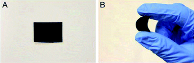 | ||
| Fig. 1 Optical images of flexible CNT bulky papers. | ||
The morphology and nanostructures of the bulky papers were characterized using field emission scanning electron microscopy (FESEM) (JEOL JSM-7600F). The TEM samples were prepared by dropping the CNT solution onto a copper grid, which were then examined using transmission electron microscopy (TEM) (JEOL JEM-2100F). The Raman spectra were obtained with a WITec CRM200 confocal Raman microscopy system with a laser wavelength of 488 nm and a spot size of 0.5 mm. The Si peak at 520 cm−1 was used as a reference to calibrate the wavenumber. The absorption spectra were obtained using a UV spectrophotometer (Shimadzu UV-3101). The Hall measurement was carried out using a Hall system (HL 5500) at room temperature under the van der Pauw mode.
The resistivity and Seebeck coefficient were measured from 323 K to 673 K using a commercially available ZEM 3 Seebeck meter under a helium environment. The CNT bulky paper was cut to a rectangular piece with dimensions of 10 × 4 mm2. Next, the bulky paper was fixed onto a glass substrate by applying silver paste to both ends. The samples for the thermal conductivity measurement were cut into 12.7 × 12.7 mm2 pieces and were measured by laser flash method (NETZSCH MicroFlash LFA457).27,28 The specific heat, Cp, was determined using the comparison method with a standard sample (POCO graphite) tested under the same conditions.29 The density, ρ, was measured by the Archimedes method and the thermal conductivity, κ, was calculated using the equation, κ = D × ρ × Cp. Here, the thermal conductivity measurements were verified in two different groups and carried out by different people.
3. Results and discussion
3.1. Structural characterization
The field emission scanning electron microscopy (FESEM) observations indicated that the CNTs were entangled randomly and network structures were formed (Fig. 2A–C). The high resolution transmission electron microscopy (HRTEM) images (Fig. 2D–F) indicated that the CNTs clearly showed structural differences after plasma treatment. The HRTEM image of the pristine CNTs (Fig. 2D) showed that the walls of the CNTs were crystalline. Upon Ar plasma irradiation for 10 s, it was observed that structural defects started to form in the crystalline CNT wall, as shown in the HRTEM image (Fig. 2E). In order to manifest this phenomenon, we extended the plasma treatment time to 60 s. The degree of the structural disorder in the CNT walls increased further to form amorphous structures (Fig. 2F). Therefore, increasing the plasma treatment time can lead to more structural defects generated in the CNT walls, and controlling the plasma treatment time could tailor the amount of defects created in the CNTs.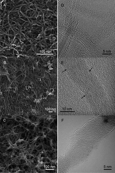 | ||
| Fig. 2 FESEM images of CNTs (A) before and (B–C) after Ar plasma treatment for (B) 10 s and (C) 30 s. HRTEM images of CNTs (D) before and (E–F) after Ar plasma treatment for (E) 10 s and (F) 30 s. The defects in (E) are marked by the arrows. | ||
Raman spectroscopy was used to examine the structural defects generated in the CNTs upon Ar plasma treatment (Fig. 3A). This was revealed by the increase in the intensity ratio of the D band (1331 cm−1) to the G band (1580 cm−1), i.e. ID/IG, (Fig. 3B). For example, ID/IG is ∼0.54 for pristine CNTs and is increased to ∼0.63, 0.75 and 0.96 for CNTs after 10 s, 20 s and 30 s plasma treatment, respectively.
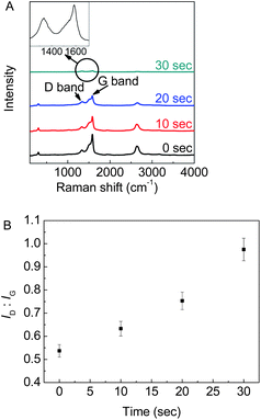 | ||
| Fig. 3 (A) Raman spectrum of CNT bulky papers after different Ar plasma treatment times. Inset: the magnified D and G bands of the CNTs after 30 s Ar plasma treatment. (B) The corresponding intensity ratio of the D band to the G band after different Ar plasma treatment times. | ||
3.2. Thermoelectric properties
The Seebeck coefficients and electrical conductivities of the Ar plasma treated CNT bulky papers were investigated (Fig. 4) in the temperature range of 300–750 K by using the commercially available ZEM-3 system. The Seebeck measurement results are plotted in Fig. 4A, indicating that all measured samples were p-type with positive Seebeck coefficients. The Seebeck coefficient of the bulky paper made of pristine CNTs did not show much variation within the temperature range measured, with a maximum value of ∼50 μV K−1 at 720 K, which is comparable with the reported value.20 After 10 s Ar plasma treatment, the maximum Seebeck coefficient of the CNT bulky paper increased to 160 μV K−1 at 670 K. By further increasing the Ar plasma treatment time to 20 s, we found that the maximum Seebeck coefficient of the CNT bulky paper could be increased remarkably to ∼350 μV K−1 at 670 K, which is more than 7 times higher than that of the pristine CNT bulky paper. For CNT bulky papers with 30 s Ar plasma treatment, the Seebeck measurement could not be successfully carried out as the electrical resistance was beyond the measurement range.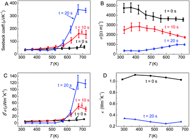 | ||
| Fig. 4 The thermal properties of SWCNT bulky papers: (A) Seebeck coefficients, (B) electrical conductivities, (C) power factors and (D) thermal conductivities of the CNT bulky papers after different Ar plasma treatment times. | ||
Although the CNT bulky papers showed enhanced Seebeck coefficients after Ar plasma treatment, their electrical conductivity decreased (see Fig. 4B). The electrical conductivity of the pristine CNT bulky paper is in the range of 3500–4800 S m−1, which decreased to values in the range of 1700–2900 S m−1 and 330–990 S m−1 for CNT bulky papers after 10 s and 20 s Ar plasma treatment, respectively. The decreased electrical conductivity was expected to be directly related to the structural defects generated in the CNTs upon Ar plasma treatment. In addition to the change in the values of the electrical conductivities, the trends of the three curves of electrical conductivity vs. temperature (Fig. 4B) are also different. The decreased electrical conductivities at high temperatures for the pristine CNT bulky paper suggested a metallic or heavily doped semiconductor characteristic.30 The increased electrical conductivities at high temperatures for the CNT bulky paper after 20 s Ar plasma treatment revealed a semiconducting behavior.
Although the electrical conductivity of the Ar-plasma treated CNT bulky paper decreased, their thermoelectric power (S2σ) increased (Fig. 4C) due to the large enhancement in the Seebeck coefficient. The maximum power factor of the pristine CNT bulky paper was 11.61 μW m−1K−2, which increased to >120 μW m−1K−2 after 20 s of plasma treatment.
The thermal conductivity of the CNT bulky paper was also investigated (Fig. 4D). Here, the samples were tested in two different groups to verify the results, which resulted in consistent data. The thermal conductivity of the pristine CNT bulky paper was about 1 W m−1 K−1 within the measurement temperature range of 290–675 K, which is comparable to the previously reported value.31 It is generally recognized that CNTs possess very high thermal conductivity, e.g. 1500 W m−1 K−1 for SWCNTs,19,32 which is one of the characteristics that makes them unsuitable for thermoelectric applications. However, when the CNTs were processed into pellets or random networks, the thermal conductivity is much lower, e.g. 1.6–2.3 W m−1 K−1 for a random network CNT pellet.31 This is mainly due to the random network of CNTs that creates many interfaces in the sample to interfere with phonon transport. The thermal conductivity of CNT bulky paper after 20 s Ar plasma treatment was 0.28–0.34 W m−1 K−1 in the measurement temperature range, which is about 3 times lower than that of the pristine one. The significant reduction in the thermal conductivity of the Ar plasma treated CNT bulky paper is mainly attributed to the generation of structural defects in the CNT walls, as illustrated by the HRTEM observations (Fig. 2D–F).
Based on the measurements of the Seebeck coefficients, electrical conductivities and thermal conductivities, the ZT values were calculated (Fig. 5). It is worth noting here that the data of the three properties for the ZT calculation were collected from the same sample. The maximum ZT value of the pristine CNT bulky paper was 0.0017–0.0062, which is similar to the previously reported data. The maximum ZT value increased by more than 60 times to ∼0.4 for the 20 s Ar plasma treated CNT bulky paper. This ZT value is still much lower than that of some of the state-of-art thermoelectric materials reported previously, e.g. 2.2 for LAST,14 1.4 for BiSbTe,1 2.4 for the Bi2Te3/Sb2Te3 superlattice,33 0.6 for Si nanowires,10 1.5 for Ti doped PbTe,13 and 1.48 for In4Se3.34 However, this value is comparable to most of the oxide thermoelectric materials for power conversion applications.35,36 Also, the easy process of preparing CNT bulky paper and its mechanical flexibility/durability could make it a new type of thermoelectric material for some niche applications with an acceptable ZT value.
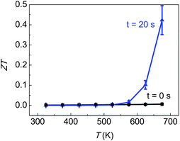 | ||
| Fig. 5 ZT values of the CNT bulky papers before and after 20 s Ar plasma treatment. | ||
It was suggested that the change in the values of S, σ and κ was closely related to (1) the variation of the carrier concentration and (2) the change in the structural order after the plasma treatment. The change in the carrier concentration was confirmed by the Hall measurement (Fig. 6). It was found that the carrier density (Fig. 6A) decreased by about two orders of magnitude after 20 s Ar plasma treatment, e.g. from 2.59 × 1022 cm−3 to 1.34 × 1020 cm−3. The decrease in the carrier concentration after plasma treatment may due to the elimination of the metallic species. In Fig. 6C, the absorption spectra of the 4 samples with different Ar plasma processing times show that the peak of the SWCNT (6,6), which is the metallic species, disappeared after 20 s and 30 s Ar plasma treatment, but the peaks of the semiconducting species (6,5) still remained.37 Thus, the Hall coefficient of the sampled treated for 20 s (e.g. 1.275 × 10⁶ m3C−1) was larger than that of the pristine CNTs (e.g. 6250 m3C−1) (Fig. 6B), which indicated a stronger semiconducting property.
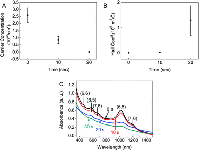 | ||
| Fig. 6 (A) Carrier concentration, (B) Hall coefficient, and (C) absorption spectra of 0 s, 10 s and 20 s Ar plasma treated CNTs. | ||
Meanwhile, the structural disorder as induced by the Ar plasma may also (1) increase the phonon scattering to decrease the thermal conductivity, (2) enhance the energy filtering effect to increase the Seebeck coefficient38 and (3) increase the scattering of the electron to decrease the electrical conductivity. The expected changes in the values of S, σ and κ as discussed above, based on the changes of (1) the charge carrier concentration and (2) the CNT structure, were consistent with the experimental observations.
3.3. Modeling
Based on the experimental results of the Seebeck coefficient, electrical conductivity and thermal conductivity, the modeling calculation using the tight-binding model39 was also carried out to provide an understanding of the observed results.The SWCNT sheets used in our experiments are mainly composed of (6,5) SWCNTs, with large tube diameters of about 7.45 Å. For simplicity, neglecting curvature effects, the dispersion relation of the tight-binding model Hamiltonian for a (n,m) SWCNT can be expressed by39

 is the magnitude of the translation vector
  , where d0 = a(n2 + m2 + nm)1/2/π is the tube diameter. υ = 1, 2, …,N, corresponds to the discrete part of the wave vector, i.e. the band index, k, is the continuous part of the wave vector, with
The relation of the band gaps to the diameter and chirality of the SWNT can be approximately given by
Fig. 7 shows the modeling results for the Seebeck coefficient, electrical conductivity and thermal conductivity, which can be described by Kubo's formula as:40
and the transport function is given by
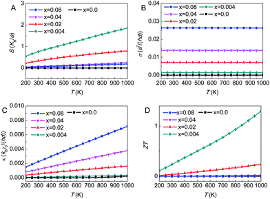 | ||
| Fig. 7 The modeling results of the plasma treated CNTs at different charge carrier densities, x (units: cm−2): (A) The Seebeck coefficient, (B) electric conductivity, (C) thermal conductivity, and (D) the ZT value. | ||
The units are: kBe ∼ 86 μV K−1, e2/hd ∼ 1.292 × 10⁵S m−1 (d ∼ 0.3 nm is the distance between the nearest neighboring CNTs),41 and kBγ0/hd ∼ 32.21 W K−1 m−1.
The calculated Seebeck coefficient increased with a decreasing carrier concentration. The obtained linear dependence of the Seebeck coefficient on the temperature deviated from the trend of the experimental curve. We attributed the deviation to the strong impurity scattering in the CNT films as the defects increased due to the plasma treatment. Meanwhile, the corresponding electrical conductivity clearly showed that the electrical conductivity decreased with a decrease in the carrier concentration. The difference between the calculated electrical conductivities with the experimental data was less than one order of magnitude. The calculated thermal conductivity, κ, decreased for the samples with lower carrier concentrations. The Hall measurements (Fig. 7) showed that the charge carrier decreased by two orders of magnitude after 20 s Ar plasma treatment, which led to an increase of S and a decrease of σ and κ. As a result, the dimensionless thermoelectric figure of merit, ZT (Fig. 7D) increased after the plasma treatment, which gave support to our experimental results.
Conclusions
In summary, we showed that the thermoelectric properties of the CNT bulky paper could be enhanced significantly by Ar plasma treatment. The improved thermoelectric properties are mainly due to the greatly increased Seebeck coefficient and a reduction in the thermal conductivity, although the electrical conductivity also decreased. As a result, the maximum ZT value increased from 0.01 for the pristine CNT bulky paper to 0.4 for CNT bulky papers after 20 s Ar plasma treatment. Such an improvement makes the plasma treated CNT bulky paper promising as a new type of thermoelectric material for certain niche applications as it is easily processed, mechanically flexible and durable, and chemically stable.Acknowledgements
The authors gratefully acknowledge AcRF Tier 1 RG 31/08 of MOE (Singapore), NRF2009EWT-CERP001-026 (Singapore), the Singapore Ministry of Education (MOE2010-T2-1-017), an A*STAR SERC grant 1021700144 and a Singapore MPA 23/04.15.03 RDP 009/10/102 and MPA 23/04.15.03 RDP 020/10/113 grant. H.Z. thanks AcRF Tier 2 (MOE2010-T2-1-060) in Singapore and the New Initiative fund FY 2010 (M58120031) from NTU, Singapore.References
- B. Poudel, Q. Hao, Y. Ma, Y. Lan, A. Minnich, B. Yu, X. Yan, D. Wang, A. Muto, D. Vashaee, X. Chen, J. Liu, M. S. Dresselhaus, G. Chen and Z. Ren, Science, 2008, 320, 634 CrossRef CAS
.
- M. S. Dresselhaus, G. Chen, M. Y. Tang, R. Yang, H. Lee, D. Wang, Z. Ren, J.-P. Fleurial and P. Gogna, Adv. Mater., 2007, 19, 1043 CrossRef CAS
- X. B. Zhao, X. H. Ji, Y. H. Zhang, T. J. Zhu, J. P. Tu and X. B. Zhang, Appl. Phys. Lett., 2005, 86, 062111 CrossRef
- A. J. Minnich, M. S. Dresselhaus, Z. F. Ren and G. Chen, Energy Environ. Sci., 2009, 2, 466 CAS
- W. Zhou, J. Zhu, D. Li, H. H. Hng, F. Y. C. Boey, J. Ma, H. Zhang and Q. Yan, Adv. Mater., 2009, 21, 3196 CrossRef CAS
- G. J. Snyder and E. S. Toberer, Nat. Mater., 2008, 7, 105 CrossRef CAS
- N. Xiao, X. Dong, L. Song, D. Liu, Y. Tay, S. Wu, L.-J. Li, Y. Zhao, T. Yu, H. Zhang, W. Huang, H. H. Hng, P. M. Ajayan and Q. Yan, ACS Nano, 2011, 5, 2749 CrossRef CAS
- Y. Chalopin, S. Volz and N. Mingo, J. Appl. Phys., 2009, 105, 084301 CrossRef
- M. Scheele, N. Oeschler, K. Meier, A. Kornowski, C. Klinke and H. Weller, Adv. Funct. Mater., 2009, 19, 3476 CrossRef CAS
- A. I. Hochbaum, R. Chen, R. D. Delgado, W. Liang, E. C. Garnett, M. Najarian, A. Majumdar and P. Yang, Nature, 2008, 451, 163 CrossRef CAS
- J. Yang, Y. Gao, J. W. Kim, Y. He, R. Song, C. W. Ahn and Z. Tang, Phys. Chem. Chem. Phys., 2010, 12, 11900 RSC
- N. Shutoh and S. Sakurada, J. Alloys Compd., 2005, 389, 204 CrossRef CAS
- J. P. Heremans, V. Jovovic, E. S. Toberer, A. Saramat, K. Kurosaki, A. Charoenphakdee, S. Yamanaka and G. J. Snyder, Science, 2008, 321, 554 CrossRef CAS
- K. F. Hsu, S. Loo, F. Guo, W. Chen, J. S. Dyck, C. Uher, T. Hogan, E. K. Polychroniadis and M. G. Kanatzidis, Science, 2004, 303, 818 CrossRef CAS
- G. Zhang, W. Wang and X. Li, Adv. Mater., 2008, 20, 3654 CrossRef CAS
- J. R. Szczech, J. M. Higgins and S. Jin, J. Mater. Chem., 2011, 21, 4037 RSC
- G. Lota, K. Fic and E. Frackowiak, Energy Environ. Sci., 2011, 4, 1592 CAS
- J. Chen, J. Z. Wang, A. I. Minett, Y. Liu, C. Lynam, H. Liu and G. G. Wallace, Energy Environ. Sci., 2009, 2, 393 CAS
- M. Akoshima, K. Hata, D. N. Futaba, K. Mizuno, T. Baba and M. Yumura, Jpn. J. Appl. Phys., 2009, 48 Search PubMed
- G.-D. Zhan, J. D. Kuntz, A. K. Mukherjee, P. Zhu and K. Koumoto, Scr. Mater., 2006, 54, 77 CrossRef CAS
- D. J. Yang, Q. Zhang, G. Chen, S. F. Yoon, J. Ahn, S. G. Wang, Q. Zhou, Q. Wang and J. Q. Li, Phys. Rev. B: Condens. Matter, 2002, 66, 165440 CrossRef
- C. Yu, Y. S. Kim, D. Kim and J. C. Grunlan, Nano Lett., 2008, 8, 4428 CrossRef CAS
- C. Meng, C. Liu and S. Fan, Adv. Mater., 2010, 22, 535 CrossRef CAS
- D. Kim, Y. Kim, K. Choi, J. C. Grunlan and C. Yu, ACS Nano, 2010, 4, 513 CrossRef CAS
- K. Esfarjani, M. Zebarjadi and Y. Kawazoe, Phys. Rev. B: Condens. Matter Mater. Phys., 2006, 73, 085406 CrossRef
- G. U. Sumanasekera, B. K. Pradhan, H. E. Romero, K. W. Adu and P. C. Eklund, Phys. Rev. Lett., 2002, 89, 166801 CrossRef CAS
- S. Krukowski, A. Witek, J. Adamczyk, J. Jun, M. Bockowski, I. Grzegory, B. Lucznik, G. Nowak, M. Wróblewski, A. Presz, S. Gierlotka, S. Stelmach, B. Palosz, S. Porowski and P. Zinn, J. Phys. Chem. Solids, 1998, 59, 289 CrossRef CAS
- K. Shinzato and T. Baba, J. Therm. Anal. Calorim., 2001, 64, 413 CrossRef CAS
- J. Xue and R. Taylor, Int. J. Thermophys., 1993, 14, 313 CrossRef CAS
- J. Chen, T. Sun, D. Sim, H. Peng, H. Wang, S. Fan, H. H. Hng, J. Ma, F. Y. C. Boey, S. Li, M. K. Samani, G. C. K. Chen, X. Chen, T. Wu and Q. Yan, Chem. Mater., 2010, 22, 3086 CrossRef CAS
- H. Xie, J. Mater. Sci., 2007, 42, 3695 CrossRef CAS
- M. Fujii, X. Zhang, H. Xie, H. Ago, K. Takahashi, T. Ikuta, H. Abe and T. Shimizu, Phys. Rev. Lett., 2005, 95, 065502 CrossRef
- R. Venkatasubramanian, E. Siivola, T. Colpitts and B. O'Quinn, Nature, 2001, 413, 597 CrossRef CAS
- J.-S. Rhyee, K. H. Lee, S. M. Lee, E. Cho, S. I. Kim, E. Lee, Y. S. Kwon, J. H. Shim and G. Kotliar, Nature, 2009, 459, 965 CrossRef CAS
- T. Sun, J. Ma, Q. Y. Yan, Y. Z. Huang, J. L. Wang and H. H. Hng, J. Cryst. Growth, 2009, 311, 4123 CrossRef CAS
- T. Sun, H. H. Hng, Q. Y. Yan and J. Ma, J. Appl. Phys., 2010, 108, 083709 CrossRef
- J. Zhao, C. W. Lee, X. Han, F. Chen, Y. Xu, Y. Huang, M. B. Chan-Park, P. Chen and L.-J. Li, Chem. Commun., 2009, 7182 RSC
- J. M. O. Zide, D. Vashaee, Z. X. Bian, G. Zeng, J. E. Bowers, A. Shakouri and A. C. Gossard, Phys. Rev. B: Condens. Matter Mater. Phys., 2006, 74, 205335 CrossRef
- J. W. Ding, X. H. Yan and J. X. Cao, Phys. Rev. B: Condens. Matter, 2002, 66, 073401 CrossRef
- G. Pálsson and G. Kotliar, Phys. Rev. Lett., 1998, 80, 4775 CrossRef
- A. I. Zhbanov, E. G. Pogorelov and Y.-C. Chang, ACS Nano, 2010, 4, 5937 CrossRef CAS
Footnote |
| † Electronic supplementary information (ESI) available: modelling of the thermoelectric properties. See DOI: 10.1039/c1ee01931g |
| This journal is © The Royal Society of Chemistry 2012 |