Enhanced formation of PbSe nanorodsvia combined solution–liquid–solid growth and oriented attachment†
Min-Seok
Kim
and
Yun-Mo
Sung
*
Department of Materials Science and Engineering, Korea University, Anam-Dong 5-1, Seoul, 136-713, South Korea. E-mail: ymsung@korea.ac.kr; Fax: +82 2 928 3584; Tel: +82 2 3290 3286/3817
First published on 16th January 2012
Abstract
With the aid of Bi catalysts dispersed in a precursor solution, PbSe nanorods were successfully synthesized by solution–liquid–solid (SLS) growth of PbSe nanocrystals followed by oriented attachment of adjacent PbSe nanoparticles. The processing temperature and time for the nanorod synthesis were markedly reduced to 180 °C and 1 min, respectively. The as-synthesized PbSe nanorods were in necklace shapes with ∼10 to 20 nm in diameter and ∼400 to 700 nm in length. The nanorods were highly crystalline, showing 〈100〉 preferential growth orientation. The exactly identical experimental conditions excluding Bi catalysts produced only spherical shape PbSe nanoparticles with ∼10 nm in diameter. The primary PbSe nanocrystals produced by Bi catalystsviaSLS growth could have net dipole moments due to the elongation into 〈100〉 orientation and they can attract nearby Bi catalyst-free PbSe nanoparticles successively to grow into one-dimensional nanorods.
Introduction
Solution-based crystal growth has recently emerged as an important route for semiconductor nanorod or nanowire synthesis, since it is advantageous in some critical aspects compared to common vapor-phase growth such as vapor–solid (VS) and vapor–liquid–solid (VLS) growth.1,2 First, it is possible to obtain highly crystalline nanowires at low growth temperatures. This facilitates the use of various kinds of substrates such as metals having low melting points, polymers, and transparent conducting oxide (FTO, ITO, AZO, etc.) coated glasses.3,4 Second, specific features can be acquired by controlling precursors, surfactants, or growth kinetics.5–9 There have been some examples of success in synthesizing unique morphologies between one- and two-dimensional nanocrystals. Third, solution-based growth can lead to a high production yield, therefore it is easy to be scaled up.10,11 For this reason, the solution-based methods seem to be very promising among currently used nanorod or nanowire synthesis routes. Template-based synthesis,12,13 solvothermal/hydrothermal synthesis,14 solution–liquid–solid (SLS) growth,15–18 and oriented attachment growth are generally regarded as representatives of the solution-based synthesis.Among them, attention has been paid to the oriented attachment growth, which refers to the phenomenon that nanoparticles align with some specific forces, subsequently attaching to each other, and finally forming one-dimensional nanorods/nanowires. Although some studies exist related to the oriented attachment growth and they gave scientific reasons for the above mentioned forces like surface energy (dangling bonds) and dipole moment, the reasons are not definite and further studies are required for its general application to other systems.19–25 This interesting phenomenon has been observed for several one-dimensional materials such as ZnO,19 ZnS,20CdSe,21CdTe,22 and PbSe.23–25 Up to now, the formation of PbSe nanorods and their growth mechanism have been intensively explored by Murray et al.23–25 They propose that the formation of dipole moment along with the 〈100〉 axis is the most probable in PbSe nanoparticles and it originates from the lack of central symmetry in the cubic crystal structure. As a result small PbSe nanoparticles of ∼4 to 5 nm can form nanorods. On the other hand they have also found that PbSe nanoparticles having ∼10 nm size could not form nanorods probably since the large particles maintain the cubic symmetry.
PbSe has a direct energy band gap of 0.28 eV in the bulk state and it has the cubic structure of rock salt. And it shows high electron (1020 cm2 V−1 s−1 at room temperature) and hole (930 cm2 V−1 s−1 at room temperature) mobility and a high figure of merit in thermoelectricity.26,27 Therefore, it can be used for infrared detectors, high-performance field-effect transistors (FETs), thermoelectric (TE) devices, etc.23
Here, we report that bismuth (Bi) nanoparticle catalysts added in the precursor solution can enhance the oriented attachment of large size PbSe nanoparticles. Using the Bi nanoparticle catalysts, we successfully synthesized the PbSe nanorods with ∼10 to 20 nm in diameter at a relatively low temperature (180 °C) and within very short time (l min). We propose a probable hypothesis for this enhanced oriented attachment growth and it is supported by additional experiments conducted excluding the Bi catalysts.
Experimental procedure
All chemicals except TDPA (Alfa Aesar) were purchased from Sigma-Aldrich and used as received. The preparation method of the Bi nanoparticles is summarized in the ESI†. 0.134 g of lead(II) oxide (PbO, ≥99.0%), 10 mL of 1-octadecene (ODE, ≥95.0%), 2 mL of oleic acid (OA, 90%), and 0.1 g of 1-tetradecylphosphonic acid (TDPA, 98%) were loaded in a 100 mL three-neck flask. TOP/Se stock solution was prepared by dissolving 1.58 g of selenium (Se, ≥95.0%) in 30 mL of trioctylphosphine (TOP, 90%) under ultrasonication. And TOP/Se/Bi solution was prepared by mixing 30 mL of TOP/Se solution with 2 mL of as-prepared TOP/Bi. The temperature of the mentioned three-neck flasks was raised to 130 °C with stirring until the complete dissolution of the PbO compounds. The synthesis method of Bi nanoparticles was mentioned in the ESI†. When the yellow mixture turned to colorless owing to the complete dissolution of the PbO compounds, the solution was heated to 180 °C with stirring. TOP/Se and TOP/Se/Bi solutions were rapidly injected into the three-neck flasks for the synthesis of PbSe nanoparticles or nanorods, respectively, and each reaction was continued for 1 min with stirring. After 1 min, each solution was cooled to the room temperature within 1 min. Each solution was purified using a mixture of ethanol and toluene and the precipitate was collected by centrifugation. This purification step was repeated several times. All the reaction steps were conducted under the flow of argon gas.The crystallinity of the samples was investigated using X-ray diffraction (XRD; Rigaku D/MAX-2500 V/PC, Tokyo, Japan). The morphologies were monitored using field emission scanning electron microscopy (FESEM; Hitachi S-4300, Tokyo, Japan). High resolution transmission electron microscopy (HRTEM; FEI Tecnai G2 F30, 300 kV) was used to examine the detailed morphologies, crystallinity, and growth orientations. Fast Fourier transform (FFT) of the images was conducted to identify the crystalline structures and growth orientations. Energy dispersive X-ray spectroscopy (EDS) attached to HRTEM was also conducted at an accelerating voltage of 300 kV to identify specific elements.
Results and discussions
The crystallinity and phase of PbSe nanorods were investigated using X-ray diffraction (XRD) as shown in Fig. 1a. XRD patterns are in good agreement with the standard diffraction data from cubic PbSe (JCPDS no. 78-1903). There exist no secondary phase peaks and the crystallinity is indeed higher than any other research having been attempted to synthesize PbSe nanowires or nanorods.16,23 The relative intensity ratio of (200) diffraction to other diffractions is higher compared to reference data (JCPDS card) and this indicates that the PbSe nanorods preferentially grew along the 〈100〉 crystallographic orientation. In the case of nanorod synthesis, ∼10 nm Bi nanoparticles were used as catalysts. The details of the synthesis method and XRD and TEM results are provided in the ESI†. Unlike the nanorods, XRD patterns reveal a different aspect when the Bi catalysts were not involved in the PbSe synthesis steps as shown in Fig. 1b. Diffraction peak broadening was noticed in each pattern and no preferential growth was detected. This could arise from the formation of PbSe nanoparticles instead of nanorods. An average crystal size was estimated as ∼10 nm using Scherrer's equation.28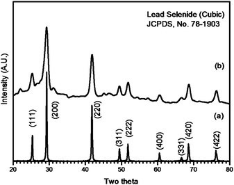 | ||
| Fig. 1 XRD patterns of (a) PbSe nanorods and (b) PbSe nanoparticles, respectively. | ||
Fig. 2 shows transmission electron microscopy (TEM) images of the PbSe nanoparticles synthesized without using Bi catalysts. As shown in Fig. 2a, the PbSe nanoparticles were spherical and they were well dispersed without agglomeration. The nanoparticles have mean diameters in the range of 9–12 nm as shown in Fig. 2b, which is consistent with the XRD results. In addition, high resolution TEM (HRTEM) images show an inter-atomic planar distance of 0.22 nm, which is in good agreement with that of the (220) plane of bulk PbSe as shown in Fig. 2c. Fast Fourier transform (FFT) of an image also verifies that the PbSe nanoparticles have a high crystalline cubic structure as shown in the inset of Fig. 2c.
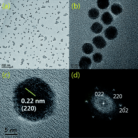 | ||
| Fig. 2 (a) An overall TEM image of as-synthesized PbSe nanoparticles. (b) A high resolution TEM image showing the particle size of 9–12 nm. (c) A high resolution TEM image showing (220) planes of the PbSe nanoparticles and (d) the corresponding FFT pattern showing the cubic symmetry, respectively. | ||
The Bi nanoparticles with the size of ∼10 nm were used to synthesize PbSe nanorods. Using a field-emission scanning electron microscope (FESEM), we confirmed that Bi catalysts exist at the PbSe nanorod tips. Compared with the PbSe nanocrystals, Bi catalysts are brighter in contrast to the image shown in Fig. 3a and this phenomenon results from the difference in the electron scattering according to elements or compounds. As presented in Fig. 3b, the diameter and the length of nanorods were 10–20 nm and 400–700 nm, respectively. The nanorods were not agglomerated with each other and there exists a small amount of PbSe nanoparticles which could not take part in the formation of the PbSe nanorods. The energy dispersive X-ray spectroscopy (EDS) data taken from the tip of PbSe nanorods show the existence of Bi, Pb and Se elements (Fig. 3c). And this reveals that Pb and Se atoms were solubilized inside the molten Bi catalysts during the synthesis. EDS spectra also show that the middle part of PbSe nanorods has only Pb and Se elements without Bi as shown in Fig. S3b†. Based upon Fig. S3† and 3 revealing waved shapes and series of tiny segments of nanorods, we could conclude that PbSe nanorods grew by the oriented attachment mechanism. The oriented attachment growth of PbSe nanorods is more vivid in Fig. 3a.
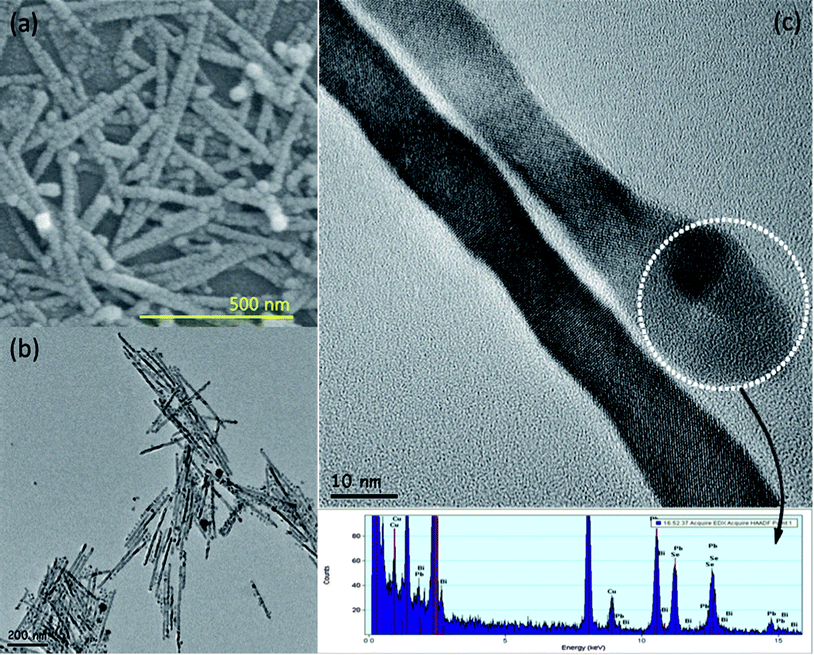 | ||
| Fig. 3 High resolution (a) SEM and (b) TEM images of PbSe nanorods synthesized using the Bi catalysts. (c) A magnified HR-TEM image and EDS data showing the Bi tip and its elemental analysis, respectively. | ||
As shown in Fig. 4, the fringe images and their pertinent FFT patterns were obtained from the HRTEM image of PbSe nanorods. Interestingly, we could find different fringe images from each of the nanorods. In the case of Fig. 4, three different atomic planes were identified. Region (a) has an inter-atomic planar distance of 0.35 nm which corresponds with the (111) planes of pure PbSe. The FFT pattern of (a) also exhibits dominant dot diffraction patterns along (111) planes. In region (b), the inter-atomic planar distance is 0.31 nm which corresponds to (200) planes. In region (c) the mixture of (200) and (![[1 with combining macron]](https://www.rsc.org/images/entities/char_0031_0304.gif) 11) planes of pure PbSe were identified ((11) is the relative index of (111)). And the FFT pattern of each region has the strong dot patterns along its specific crystallographic orientation. The observation of numerous samples using HRTEM and FFT demonstrates that the PbSe nanorods are preferentially 〈100〉 oriented single crystals. Fig. 4 also reveals the 〈100〉 crystallographic orientation growth of PbSe nanorods based on vector calculation and analysis of FFT patterns and this result is consistent with the XRD analysis as shown in Fig. 1a. To summarize, the synthesized PbSe nanorods exhibited single and high crystallinity, although they consisted of crystallographically different regions along the 〈100〉 axis in the HRTEM images. And the waved morphology gives the evidence for the oriented attachment growth as presented in previous articles.23–25
11) planes of pure PbSe were identified ((11) is the relative index of (111)). And the FFT pattern of each region has the strong dot patterns along its specific crystallographic orientation. The observation of numerous samples using HRTEM and FFT demonstrates that the PbSe nanorods are preferentially 〈100〉 oriented single crystals. Fig. 4 also reveals the 〈100〉 crystallographic orientation growth of PbSe nanorods based on vector calculation and analysis of FFT patterns and this result is consistent with the XRD analysis as shown in Fig. 1a. To summarize, the synthesized PbSe nanorods exhibited single and high crystallinity, although they consisted of crystallographically different regions along the 〈100〉 axis in the HRTEM images. And the waved morphology gives the evidence for the oriented attachment growth as presented in previous articles.23–25
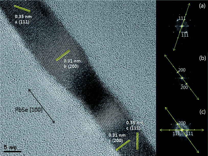 | ||
| Fig. 4 A highly magnified HR-TEM image showing (a) (111) planes, (b) (200) planes and (c) the mixture of (200) and (11) planes, respectively. The insets show the corresponding FFT patterns of (a), (b), and (c), respectively. | ||
Through the examination of our experimental data, we could conclude that the Bi catalysts induced the oriented attachment of the PbSe nanorods. To explain this phenomenon clearly, we focused on experimental conditions. First, the processing temperature was very low (180 °C) compared with the previously reported papers (∼250 °C). Second, the reaction was completed within 1–2 min and this processing time is shorter than any other report. Third, Pb![[thin space (1/6-em)]](https://www.rsc.org/images/entities/char_2009.gif) :Se, the reactant ratio was about 1:1. For the high-yield synthesis of PbSe nanorods, people have usually used the Pb:Se ratio higher than 1:1.23,25 Based upon these facts, the possible mechanism of the PbSe nanorod growth was proposed for the samples with Bi catalysts.
:Se, the reactant ratio was about 1:1. For the high-yield synthesis of PbSe nanorods, people have usually used the Pb:Se ratio higher than 1:1.23,25 Based upon these facts, the possible mechanism of the PbSe nanorod growth was proposed for the samples with Bi catalysts.
At the initial stage of the reaction, Pb and Se atoms penetrate into the Bi catalysts until supersaturation of Bi occurs. The melting point of bulk Bi is 271 °C and the reaction took place at 180 °C. However, Pb and Bi can form the eutectic point at 128 °C (Fig. S4†).30 Moreover, the melting temperature of Bi nanoparticles itself can drop to 225 °C when their size reaches down to ∼10 nm.29 Therefore, the molten Bi alloy catalysts could act as the energetically favored sites and absorb precursors. After the supersaturation occurred, PbSe crystals could nucleate and grow from the Bi alloy catalysts by the solution–liquid–solid (SLS) growth mechanism. On the other hand, Pb and Se atoms in the precursor solution can independently combine with each other to form PbSe nanoparticles at 180 °C, and this temperature has been known to the appropriate condition to form PbSe nanoparticles as verified in some papers.16,23 The above mentioned processes are depicted in Fig. 5a. Pure PbSe crystals have the rock salt structure. Recently, Murray et al. proposed a reasonable mechanism regarding the oriented attachment growth of PbSe nanorods.25 They explained that it is more possible to lack the central symmetry and possess a dipole moment along the 〈100〉, 〈110〉, or 〈111〉 axes. After the calculation of the dipole moments according to crystallographic orientations, they could conclude that the 〈100〉 axis has the highest probability to induce the dipole moment in the case of relatively small PbSe nanoparticles (∼4 to 5 nm). However, the larger PbSe nanocrystals could not form nanorods. It seems that the PbSe nanoparticles of about 10 nm sizes maintained their symmetry based on the cubic structure.23 They mentioned that the largest dipolar interactions are predicted for relatively small nanocrystals. On the other hand, the large nanoparticles cannot have the net dipole moments enough to fuse into nanorods.
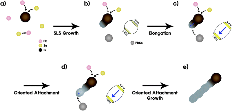 | ||
| Fig. 5 Schematic diagram presenting a suggested mechanism for the Bi catalyst induced oriented attachment growth of PbSe nanorods. (a) Penetration of Pb and Se elements into Bi catalysts and independent binding between Pb and Se elements. (b) Supersaturation and growth. (c and d) Losing cubic symmetry (dipole moment formation) and subsequent attachment of PbSe nanoparticles, respectively. (e) Final wave-shaped PbSe nanorods. | ||
In the case of our experimental processes, we synthesized ∼10 nm PbSe nanoparticles and could easily reach the oriented attachment growth using the Bi catalysts. Hence, a different growth mechanism had to be suggested for our finding. During the initial stage of SLS growth (Fig. 5a), PbSe nanocrystals tend to nucleate and grow along the 〈100〉 direction after the supersaturation occurs as already shown by Kuno's group.16 During this reaction, the PbSe nanocrystals having the cubic structure are elongated along the 〈100〉 direction due to the continuous supply of Pb and Se atoms to the Bi catalysts for SLS growth as depicted in Fig. 5b and c. Some surfactants show selective binding to specific facets of nanocrystals and hinder the growth of the specific facets, resulting in the growth of one-dimensional nanorod or nanowire structures. In our case TOP and/or TDPA could induce the 〈100〉 elongation of the primary PbSe nanocrystals nucleated from Bi catalystsviaSLS. As a result, the elongation permits the PbSe nanocrystals to have the net dipole moments towards the 〈100〉 direction and induce the subsequent attachment of the nearby PbSe nanoparticles independently synthesized as presented in Fig. 5d. This driving force, which means the dipole moment or the loosing symmetry, could cause another dipole moment in the adjacent PbSe nanoparticles like a domino and oriented attachment could continue. Finally, the PbSe nanorods having 400–700 nm length could form as shown in Fig. 5e.
Conclusions
The PbSe nanorods having high crystallinity and single crystallinity were successfully synthesized using the Bi catalystsvia the oriented attachment growth mechanism. PbSe nanocrystals were formed by Bi catalystsvia solution–liquid–solid (SLS) mechanism and they were slightly elongated along the <100> orientation possibly due to TOP/TDPA. The elongated PbSe nanocrystals could have net dipole moment along the 〈100〉 direction. Due to the dipole moment adjacent PbSe nanoparticles independently formed in the precursor solution were attached to the primary PbSe nanocrystals along the 〈100〉 orientation. The attached PbSe nanoparticles also could have dipole moment and they will attract next adjacent PbSe nanoparticles. Therefore, the attachment growth could continue like a domino to arrive at ∼400 to 700 nm length PbSe nanorods. Owing to the Bi catalyst the processing temperature and time could be considerably reduced to 180 °C and 1 min, respectively. Moreover, the waste of precursors, which has been usually reported in other literatures, could be prevented by adjusting the Pb:Se ratio to 1:1. Through the careful examination of the PbSe nanorods, we suggested a possible growth mechanism. This was the first finding that Bi catalysts can enhance the oriented attachment. Although this was the attempt to enhance the oriented attachment growth of PbSe using Bi catalysts, it is believed that this synthetic method can be applied to various materials based on theoretical considerations.
Acknowledgements
This work was supported by International Collaborative R&D Program (2011-BS-101002-001) funded by Ministry of Knowledge Economy (MKE) and the National Research Foundation of Korea (NRF) grant funded by the Korea government (MEST) (2011-0011205). The authors thank Dr H. S. Baik of Korea Basic Science Institute (KBSI) for providing the access of their HRTEM.Notes and references
- X. Wang and Y. Li, Inorg. Chem., 2006, 45, 7522 CrossRef CAS.
- M. Kuno, Phys. Chem. Chem. Phys., 2008, 10, 620 RSC.
- A. Nadarajah, R. C. Word, J. Meiss and R. Könenkamp, Nano Lett., 2008, 8, 534 CrossRef CAS.
- W.-C. Kwak, S.-H. Han, T. G. Kim and Y.-M. Sung, Cryst. Growth Des., 2010, 10, 5297 CAS.
- X. Peng, L. Manna, W. Yang, J. Wickham, E. Scher, A. Kadavanich and A. P. Alivisatos, Nature, 2000, 404, 59 CrossRef CAS.
- X. Peng, Adv. Mater., 2003, 15, 459 CrossRef CAS.
- S. Chen, Z. L. Wang, J. Ballato, S. H. Foulger and D. L. Carroll, J. Am. Chem. Soc., 2003, 125, 16186 CrossRef CAS.
- J. Tang and A. P. Alivisatos, Nano Lett., 2006, 6, 2701 CrossRef CAS.
- Y.-W. Jun, J.-S. Choi and J. Cheon, Angew. Chem., Int. Ed., 2006, 45, 3414 CrossRef CAS.
- U. Jeong, Y. Xia and Y. Yin, Chem. Phys. Lett., 2005, 416, 246 CrossRef CAS.
- L. Cademartiri, J. Bertolotti, R. Sapienza, D. S. Wiersma, G. V. Freymann and G. A. Ozin, J. Phys. Chem. B, 2006, 110, 671 CrossRef CAS.
- D. Xu, D. Chen, Y. Xu, X. Shi, G. Guo, L. Gui and Y. Tang, Pure Appl. Chem., 2000, 72, 127 CrossRef CAS.
- G. Cao and D. Liu, Adv. Colloid Interface Sci., 2008, 136, 45 CrossRef CAS.
- G. Zou, H. Li, Y. Zhang, K. Xiong and Y. Qian, Nanotechnology, 2006, 17, S313 CrossRef CAS.
- T. J. Trentler, K. M. Hickman, S. C. Goel, A. M. Viano, P. C. Gibbons and W. E. Buhro, Science, 1995, 270, 1791 CAS.
- K. L. Hull, J. W. Grebinski, T. H. Kosel and M. Kuno, Chem. Mater., 2005, 17, 4416 CrossRef CAS.
- F. Wang, A. Dong, J. Sung, R. Tang, H. Yu and W. E. Buhro, Inorg. Chem., 2006, 45, 7511 CrossRef CAS.
- W.-C. Kwak, T. G. Kim, W. Lee, S.-H. Han and Y.-M. Sung, J. Phys. Chem. C, 2009, 113, 1615 CAS.
- C. Pacholski, A. Kornowski and H. Weller, Angew. Chem., Int. Ed., 2002, 41, 1188 CrossRef CAS.
- N. Pradhan and S. Efrima, J. Phys. Chem. B, 2004, 108, 11964 CrossRef CAS.
- N. Pradhan, H. Xu and X. Peng, Nano Lett., 2006, 6, 720 CrossRef CAS.
- Z. Tang, N. A. Kotov and M. Giersig, Science, 2002, 297, 237 CrossRef CAS.
- K.-S. Cho, D. V. Talapin, W. Gaschler and C. B. Murray, J. Am. Chem. Soc., 2005, 127, 7140 CrossRef CAS.
- Q. Zhang, S.-J. Liu and S.-H. Yu, J. Mater. Chem., 2009, 19, 191 RSC.
- W.-K. Koh, A. C. Bartnik, F. W. Wise and C. B. Murray, J. Am. Chem. Soc., 2010, 132, 3909 CrossRef CAS.
- C. Kittel, Introduction to Solid State Physics, John Wiley & Son, New York, 8th edn, 2005 Search PubMed.
- G. Min and D. M. Rowe, J. Mater. Sci. Lett., 1997, 16, 1339 CrossRef.
- B. D. Cullity and S. R. Stock, Elements of X-Ray Diffraction, Prentice Hall, NJ, 3rd edn, 2001 Search PubMed.
- S. S. Dalgic, J. Optoelectron. Adv. Mater., 2009, 11, 2133 CAS.
- H. Okamoto, J. Phase Equilib., 1994, 15, 361 CAS.
Footnote |
| † Electronic supplementary information (ESI) available. See DOI: 10.1039/c2ce06353k |
| This journal is © The Royal Society of Chemistry 2012 |