 Open Access Article
Ultra-thin conductive free-standing PEDOT/PSS nanofilms†
Francesco
Greco
*a,
Alessandra
Zucca
ab,
Silvia
Taccola
ab,
Arianna
Menciassi
ab,
Toshinori
Fujie
ac,
Hiroki
Haniuda
c,
Shinji
Takeoka
c,
Paolo
Dario
ab and
Virgilio
Mattoli
*a
aCenter for MicroBioRobotics @SSSA, Istituto Italiano di Tecnologia, Viale Rinaldo Piaggio 34, 56025, Pontedera (PI), Italy. E-mail: francesco.greco@iit.it; virgilio.mattoli@iit.it; Fax: +39 050 883101; Tel: +39 050 883417
bBiorobotics Institute, Scuola Superiore Sant'Anna, Polo Sant'Anna Valdera, Viale Rinaldo Piaggio 34, 56025, Pontedera (PI), Italy
cDepartment of Life Science and Medical Bioscience, Graduate School of Advanced Science and Engineering, Waseda University, TWIns, 2-2 Wakamatsu-cho, Shinjuku-ku, 162-8480, Tokyo, Japan
First published on 11th October 2011
Abstract
Free-standing conductive ultra-thin films based on poly(3,4-ethylenedioxythiophene)/poly(styrenesulfonate) (PEDOT/PSS) are realized. A fabrication process based on a modified Supporting Layer technique is proposed that provides for the easy production of conductive nanofilms having a very large surface area with typical thickness of tens of nanometres. The proposed free-standing nanofilms can be manipulated, folded and unfolded in water many times without suffering from cracks, disaggregation or from loss of conductive properties. After collecting them onto rigid or soft substrates, they retain their functionality. Structural and functional properties of the nanofilms are described by means of their thickness, topography, conductivity and Young's modulus. Strong dependences of these properties on residual water, post-deposition treatments and environmental moisture are clearly evidenced. Possible applications are foreseen in the field of sensing and actuation, as well as in the biomedical field, e.g. as smart substrates for cell culturing and stimulation.
1. Introduction
Since their original discovery and the pioneering research in the 70s and the 80s1–3 conductive polymers have gathered considerable attention due to a number of attractive features: tunability of physical properties, flexibility, stimuli responsiveness, etc.4 Different classes of conductive polymers have been explored during the past two decades, conjugated polymers being one of the most interesting.5 In general, a drawback of employing conductive polymers is the lack of adequate methods to disperse or dissolve them in order to permit their easy manipulation and micro-/nanofabrication through relatively easy, cheap and reliable techniques (i.e.spin coating, casting, etc.), as commonly used for other classes of polymers.4 Regarding conjugated polymers, poly(3,4-ethylenedioxythiophene) (PEDOT) is one of the most employed;6,7PEDOT is known to possess both ionic and electronic conduction and it has been the subject of extensive research in different fields and proposed applications, including microelectronics, sensing, actuation, as a bio-compatible material for neural implants, biological scaffolds, optoelectronic applications, etc.8 Key features for the success of PEDOT as an attractive conductive polymer material are good conductivity and chemical stability; in addition, a very important and interesting feature for many applications is the market availability of PEDOT/PSS, the macromolecular complex of PEDOT with poly(styrenesulfonate) (PSS), as a ready-to-use waterborne dispersion of PEDOT/PSS gel particles. Conductive films in which the gel particles merge to form a continuous film under water evaporation are obtained by spin coating onto different substrates (Si, glass, ITO, etc.). PEDOT/PSS has already been proposed and successfully employed as conductive coating (e.g. antistatic protective coating), as conductive layer in multilayer structures (e.g. charge injection in OLED) or also as active material in the development of a number of sensing and actuating devices, based on its stimuli-responsive properties. PEDOT, whose biocompatibility has been proved in very recent works, has been successfully applied in the development of microelectrodes for neural interfaces as well as in scaffolds for epithelial cell adhesion and proliferation controlled by electrochemical modulation of surface properties.9,10Generally speaking, polymers in the form of thin or ultra-thin films have been intensively studied. The literature reports many different approaches towards the obtainment of polymer nanofilms, due to the peculiar characteristics of such nanostructures and to the novel effects arising in scaling polymer membranes down to nanometres. Very recently, also free-standing nanofilms have been realized and studied, having huge aspect ratio values (up to 106; tens of nanometres thick polymer membranes having surfaces of a few cm2). The achievement of very large surface, ultra-thin, flexible and robust free-standing nanofilms has been made possible through Layer-by-Layer (LbL) self-assembling techniques in spin coating or dip coating, e.g. making use of alternating polyelectrolytes.11–14 Similar polymer nanofilms have also been fabricated with polysaccharide polyelectrolytes of biological origin, such as chitosan and alginate, that have been proved to be useful in biomedical applications as surgical plasters.15 Additionally, a free-standing single layered poly(lactic acid) (PLA) nanofilm to be used as a substrate for cell-based devices or in regenerative medicine has been recently developed by our group.16
Despite the extensive use of conductive polymers in the form of ultra-thin films in many applications, also using an LbL self-assembling technique for obtaining polyelectrolyte multilayer structures,17 the fabrication of free-standing conductive polymer ultra-thin films has not been yet reported. Only very recently Choi et al. proposed a method for the fabrication of free-standing PEDOT/graphene composite nanofilm using dispersible graphene oxide in a multilayer structure.18 The described structure showed improved mechanical strength and conductivity with respect to traditional PEDOT films. However, the reported procedure is quite complex, involving many expensive, time consuming and delicate steps, such as successive oxidation and reduction steps for the formation of graphene by graphite through the intermediate formation of graphene oxide sheets.
In this paper we describe an easy fabrication method for obtaining PEDOT/PSS free-standing nanofilms and the results of their characterization in terms of surface morphology, electrical and mechanical properties. The obtainment of robust and flexible free-standing conductive polymer nanofilms is attractive for several reasons.
First of all, sensing and actuation applications can be foreseen including locomotion of micro- and meso-scale objects in water and other biological fluids, pressure and humidity sensing with totally free-standing or anchored membranes (e.g.PEDOT nanofilms suspended over micro-fabricated frames). In the fabrication of multilayer and multifunctional material structures, the capability to insert electroconductive properties is as well interesting. Additionally, by using the proposed method the deposition of nano-scale conductive films over micro- or meso-scale artifacts, biological samples and in general insulators, could be achieved through a “soft”, simple, cost effective, non-destructive technique in water. The already tested biocompatibility of PEDOT/PSS allows for considering these ultra-thin conductive polymer films to be valid substrates in the field of bio-hybrid devices; applications could be foreseen e.g. for cell adhesion, growth, differentiation, stimulation and, in general, in the fields of regenerative medicine, muscle tissue engineering and drug delivery.
More interestingly, flexible conducting polymer nanostructures, in the form of free-standing nanofilms or microfibers, could be employed as artificial substrates for the development of bio-hybrid actuating devices. In such microdevices the use of non-spontaneous contractile cell lines (e.g.myoblasts) as actuating elements, when electrically stimulated by the PEDOT nanofilms, could be combined with micromechanical systems.19–21
2. Results and discussion
2.1 Fabrication of free-standing PEDOT/PSS nanofilms
Ultra-thin free-standing PEDOT/PSS nanofilms having a very large surface/thickness ratio were prepared following a method that uses a water-soluble polymer as a supporting layer from which the nanofilm can be released.15,22Fig. 1 schematically summarizes the fabrication and recovery steps for the proposed procedure. | ||
| Fig. 1 Schematic representation of the main steps of fabrication and release for obtaining PEDOT/PSS nanofilms by a Supporting Layer technique. (a) Si substrate; (b) spin-coating deposition of the PDMS substrate layer; (c) spin-coating deposition of the PEDOT/PSS nanofilm; (d) casting of a thick PVA supporting layer; (e) cutting and (f) peeling of the bilayer (PVA supporting layer + PEDOT/PSS nanofilm); (g) free-standing PEDOT/PSS nanofilm floating in water after dissolving PVA. Detailed information on experimental parameters and processes is reported in the Experimental section. | ||
The Supporting Layer method, as originally proposed by Whitesides et al., and successfully applied to LbL assembled polysaccharide nanofilms with a large surface area by Fujie et al., enables to release and recover a free-standing nanofilm by peeling a dried bilayered film (comprising the desired nanofilm supported by a layer of a water-soluble polymer, e.g.poly(acrylic acid) (PAA) or poly(vinylalcohol) (PVA)) from a SiO2 substrate onto which the layers had been deposited by spin-coating.15,22 The removal of the ultra-thin film from the substrate is possible due to the stronger interactions between the bilayered components with respect to those between the polymer nanofilm and the SiO2 substrate.
In the present case direct deposition of PEDOT/PSS onto the SiO2 surface was tested but the nanofilm could not be peeled off together with the Supporting PVA Layer due to the strong adhesion of the nanofilm to the substrate. For this reason, the SiO2 surface has been replaced by a thin layer of poly(dimethylsiloxane) (PDMS) deposited onto a Si wafer. PDMS provided a suitable non-adhesive (repulsive) substrate for the subsequent release of the free-standing PEDOT/PSS nanofilms, due to its low surface energy.
A thin layer of PDMS (∼800 nm) was deposited onto a Si wafer following a recently reported procedure for the spin-coating of sub-micrometre thick elastomeric films.23
The wettability of the pristine PDMS surface was temporarily improved by an O2 plasma treatment just before the nanofilm deposition in order to allow the spreading of the PEDOT/PSS water dispersion and the formation of a homogeneous film by spin-coating. It is important to notice that, due to the very well known effect of hydrophobic surface recovery in siloxanes,24 the adhesion of the nanofilm to PDMS becomes poor after some hours since the film deposition, allowing its release. After the deposition of the PEDOT/PSS layer, a thermal annealing operated at T = 170 °C for 1 h is provided, making the conductive polymer nanofilm resistant to water. Besides the excellent thermal stability of PEDOT/PSS,7 this step is also known to operate a rearrangement of PEDOT and PSS microdomains.25 Indeed, heat can affect conductive properties by changing size and distances between colloidal particles in the PEDOT/PSS composite as in other granular conductors, in which conductivity is regulated via hopping transport. The number and/or height of inter-particle barriers are reduced upon heating due to softening and segregation of PSS or coalescence of PEDOT/PSS particles.
Casting of a relatively concentrated solution of PVA (10 wt% in DI water) onto the PEDOT/PSS nanofilm provided a supporting PVA layer that, when dried, could be cut with a razor blade and peeled off with the aid of tweezers from the PDMS surface as a bi-layer carrying with it the PEDOT/PSS nanofilm. The release of the PEDOT/PSS free-standing nanofilm from the peeled bi-layered film was finally obtained by dissolving the PVA supporting layer in DI water.
The resulting nanofilm floated in water having neutral buoyancy and could be handled, folded and unfolded many times by aspiration with a pipette or also by gently touching it with a tip. Depending on the choice of the substrate size and cutting geometry, nanofilms can have very large surface area (up to several cm2). Some pictures showing the release and recovery of PEDOT/PSS nanofilms are available in the ESI (Fig. S1†). The overall process is fast, cheap and easy; the release and recovery are provided in DI water, making suitable the development of biocompatible nanofilms. As regards the recovery of these large and flexible nanostructures, different procedures have been optimized that permit for safe manipulation and collection on several surfaces without suffering from damages or ruptures: rigid substrates such as Si, steel, glass as well as compliant ones, e.g. skin, elastomers, paper, or also plastic frames and metal meshes that permit the anchoring of suspended ultra-thin PEDOT/PSS nanofilms. Fig. 2 depicts some examples of large PEDOT/PSS nanofilms transferred to various substrates. The collection of a nanofilm floating in water could be accomplished via direct recovery over the desired substrate or also through the use of ring-shaped nets fabricated with a thin metal wire.
 | ||
| Fig. 2 PEDOT/PSS nanofilms transferred to various substrates: (a) free-standing PEDOT/PSS nanofilm floating in water after PVA dissolving; nanofilms collected onto (b) paper, (c) human skin and (d) flexible PDMS. SEM micrographs showing the PEDOT/PSS nanofilm collected onto (e) the porous alumina substrate (scale bar 2 μm) and (f) steel mesh (scale bar 100 μm). | ||
Nanofilms have been realized and comparatively characterized in this study by employing a specific formulation of PEDOT/PSS (namely Clevios™ PH1000, by the supplier H.C. Starck, Germany) containing a PEDOT/PSS ratio of 1![[thin space (1/6-em)]](https://www.rsc.org/images/entities/char_2009.gif) :2.5 by weight of the waterborne dispersion. The thickness for each nanofilm type has been varied by setting fabrication parameters, in order to derive structure/property relationships. Table 1 summarizes the typologies of prepared samples.
:2.5 by weight of the waterborne dispersion. The thickness for each nanofilm type has been varied by setting fabrication parameters, in order to derive structure/property relationships. Table 1 summarizes the typologies of prepared samples.
| Sample | Type | Fabrication procedure |
|---|---|---|
| a Additional thermal treatment at T = 170 °C for 1 h, after collection onto glass. | ||
| PH1000@Si | Supported | Spin-coating |
| PH1000@PDMS | Free-standing (before release) | Supporting Layer |
| PH1000@Glass | Free-standing (after release) | Supporting Layer |
| PH1000@Glass TTa | Free-standing (after release) | Supporting Layer |
2.2 Thickness and surface topography of PEDOT/PSS nanofilms
The thickness and roughness of the PEDOT/PSS nanofilms were measured by AFM topographic images. Regarding the thickness estimation, AFM scansion has been performed over a scratched area in a perpendicular direction with respect to the scratch edge (see the Experimental section). By measuring the height profile of the edge between the nanofilm (moderately rough surface) and the scratched domain (bare Si, atomically flat) it was possible to quantify the thickness of the nanofilm.This procedure, accomplished for nanofilms deposited by spin coating onto the Si surface (PH1000@Si samples), has been repeated for free-standing PEDOT/PSS nanofilms prepared with the Supporting Layer technique, after their release in water and collection onto a fresh Si substrate. An example of an AFM topographic image used for thickness estimation is available in the ESI (Fig. S4†).
Fig. 3 displays the estimated thickness as a function of spin-coating speed s, comparing the results obtained by AFM with those obtained by reflectometry (see below). As clearly displayed in Fig. 3, the nanofilm thickness shows a regular decreasing trend in the range 1000 < s < 4000 rpm, i.e. thickness decreases from t ≈ 95 nm at s = 1000 rpm to t ≈ 45 nm at s = 4000 rpm. As the spin-coating speed is further increased, s > 4000 rpm, thickness is no longer decreasing, with t ≈ 43 nm as the average value. Minimum achievable thickness of nanofilms is known to be related to the dimension of the PEDOT/PSS primary particles contained in the commercial product formulation. The thinnest films in the series, therefore, consist of a monolayer of loosely packed PEDOT/PSS primary particles or few particle agglomerates. Such result for PH1000 grade (whose precise characterization is still lacking in the literature due to its recent introduction) is in agreement with the data already reported for a commonly used PEDOT/PSS formulation, Clevios™ P AG.26 Additional details on comparison between PH1000 and P AG grades can be found in the ESI†.
 | ||
| Fig. 3 PEDOT/PSS nanofilm thickness t as a function of spin-coating speed s: comparison between AFM (solid circles) and Spectral Reflectivity (open triangles) estimation. | ||
The thickness measurement provided by AFM has been compared with the results obtained by reflectometry. Indeed, AFM characterization could only be precisely carried out on Si supported samples that provide the necessary rigid and ultra-smooth Si area to make clear the nanofilm edge profile; the same technique is therefore not suitable for PEDOT/PSS nanofilms supported on PDMS (PH1000@PDMS). For this reason thickness measurements of PDMS-supported (prior to release) or free-standing nanofilms have been obtained by thin film reflectometry and then compared with those of nanofilms deposited onto the Si surface and obtained by AFM. Data of thickness estimation are provided in Fig. 3. Thicknesses of samples estimated by the two techniques are in good agreement despite some minor discrepancies mostly seen for intermediate thickness values. This experimental evidence enabled us to consider the values of thickness obtained by AFM for all the subsequent calculations regarding resistivity and mechanical properties.
Concerning the surface topography, AFM scansions on PH1000@Si nanofilms revealed that all the samples have a uniform and ultra-smooth surface (ESI, Fig. S4a†). The average roughness, independently of the spin-coating speed, was measured as Ra = 1.02 ± 0.20 nm.
This “base” roughness is due to the grain structure made up of individual particles of PEDOT-rich cores and PSS-rich shells, well recognizable in AFM scansions performed over smaller areas and pointed out in previous studies investigating the nano-scale structure of PEDOT/PSS thin films.26–28
Interestingly, AFM measurements performed on nanofilms collected onto Si slabs and dried with a nitrogen gun after their release in water, evidenced some changes occurring in nanofilm morphology. As regards thickness, an average 12% decrease has been recorded independently of the employed spin coating speed. Such variation is not further affected by a subsequent thermal treatment operated at T = 170 °C for 1 h. A comparison of nanofilm thickness before and after release in water is available in the ESI (Fig. S7†). The decrease in thickness is associated with the loss of excess PSS in water during the nanofilm release. Excess PSS is known to segregate from the PEDOT/PSS complex and to constitute a top PSS-rich layer (whose thickness is ∼10% of total film thickness) in films prepared by spin coating.29,30 If a water rinse is provided, this excess PSS can be removed, as described by De Longchamp et al. who used X-ray reflectivity and visible-near infrared spectroscopy in order to quantify changes in thickness and composition of PEDOT/PSS films associated with such washing.31 The effect of PSS removal is further confirmed by the change of nanofilm surface topography after release in water, as observed in AFM imaging (ESI, Fig. S6 to be compared with surface topography before release, Fig. S4†). Due to the removal of the top PSS-rich layer, the grain-like structure of the film became more apparent. A moderate increase in average surface roughness is also observed, e.g. the roughness of a nanofilm sample prepared at spin coating speed s = 2000 rpm changes from Ra = 1.02 ± 0.20 nm to Ra = 1.47 ± 0.20 nm, while the thickness changes from t = 78.6 nm to t = 70.1 nm before and after release in water, respectively.
2.3 Mechanical properties of PEDOT/PSS nanofilms
Mechanical properties of the prepared PEDOT/PSS free-standing nanofilms were evaluated by “strain-induced buckling instability for mechanical measurements” (SIEBIMM),32 a technique used for the determination of the Young's modulus of polymer ultra-thin films. This technique is based on measuring the wavelength λ of the periodic wrinkles formed on the buckled surface of polymer thin films coating a relatively soft, thick elastic substrate such as PDMS. If the elastomer substrate is pre-stretched, the relaxation of strain induces the buckling of the film. By applying buckling mechanics, the elastic modulus of the film can be calculated. In the case of PEDOT/PSS nanofilms, the measured buckling wavelength λ increased depending on the increment of their thickness (Fig. 4a). | ||
| Fig. 4 Mechanical properties of the PEDOT/PSS nanofilms with different thicknesses t evaluated by the SIEBIMM measurement. (a) Buckling wavelength λ defined as the distance between two consecutive ripple maxima and (b) Young's modulus En of the PEDOT/PSS nanofilms (inset in (a) showing the typical buckling pattern of a 77.1 nm thick nanofilm as obtained by AFM topographic imaging). | ||
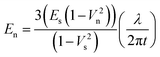
The Young's modulus (En) of the PEDOT/PSS PH1000 grade nanofilms with three different thicknesses t was obtained by using the following formula:
 | (1) |
In eqn (1), we employed the Young's modulus value of PDMS Es = 1.8 MPa, the Poisson's ratios of the PEDOT/PSS nanofilm νn = 0.33 and of the PDMS νs = 0.50, by following Rubner's report33 because the hydrophilicity of the PEDOT/PSS nanofilm was similar to that of polyelectrolyte multilayers.
By incorporating the measured wavelength λ into eqn (1) the Young's modulus of the PEDOT/PSS nanofilms En was evaluated. Results (Fig. 4b) showed En = 0.81 ± 0.1, 1.02 ± 0.1 and 1.02 ± 0.2 GPa, respectively for nanofilms with thickness t = 37.1, 58.3 and 77.1 nm (i.e. thickness after release in water, as measured for nanofilms obtained at spin coating speed s = 6000, 2500, 1500 rpm, respectively). These values are lower than Young’s moduli evaluated by SIEBIMM of conventional poly(styrene) ultra-thin films (ca. 3.5 GPa)32 and polyelectrolyte multilayer films (ca. 2.7 GPa),33 tens- to hundreds of nm in thickness. Indeed, PEDOT/PSS nanofilms were dried in vacuo prior to the SIEBIMM test in order to achieve minimum residual water content in all the tested samples, but they were then exposed to environmental conditions in order to perform the mechanical characterization; the data reported here were obtained at 50% atmospheric relative humidity. Therefore, these low Young's moduli of the PEDOT/PSS nanofilms would be derived from the moisture-sensitive nature of hydrophilic PSS, which could influence the electro-conductive properties of PEDOT/PSS nanofilms as well.
Despite the intensive use of PEDOT/PSS, so far only a few studies on its mechanical properties have been published. Okuzaki et al. performed some studies on PEDOT/PSS mechanical properties, measuring the Young's modulus and tensile strength of free-standing PEDOT/PSS samples in the form of fibers (10 μm diameter) or cast films (thickness 20–30 μm) making use of a tensile test setup.34,35 Additionally, the use of a climate chamber in which performing the tensile test permitted investigation of the mechanical behavior of PEDOT/PSS cast films (thickness ≈ 25 μm) under different relative humidity conditions and to derive some microscopic models explaining fracture behavior.36
Despite the large difference in the thickness of tested materials, the results obtained in our study with regard to the mechanical properties of the conductive nanofilms are in good agreement with those reported in the study by Lang et al.,36 in which Young's modulus of PEDOT/PSS cast films has been determined to be E = 0.9 ± 0.2 GPa, at 55% relative humidity. The finding of a value ν = 0.34 ± 0.02 for the Poisson's ratio also confirmed the value used in our calculation (νn = 0.33). The slightly lower values of E obtained in thinner nanofilms can be probably ascribed to the intrinsic structure of the nanofilm, in which a loose packing of PEDOT-rich grains is obtained as pointed out in a previous section, when discussing roughness and topography of the nanofilm surface. Here, only a few primary particles can pile up, due to the small thickness, while in thicker films interconnections between neighbor grains stacked in a “pancake-like” structure are improved, thus improving mechanical properties.27,28
On the other hand, Tahk et al., very recently reported about mechanical characterization of commonly used organic electronic materials by using a buckling technique.37 Young's modulus of PEDOT/PSS nanofilms with thickness t ≈ 50 nm spun directly on a PDMS substrate was measured to be E = 2.26 ± 0.05 GPa, a value that is slightly higher and that is comparable to the values obtained at lower relative humidity conditions (∼23 to 30% rH) in other references.34–36 Unfortunately, relative humidity conditions are not mentioned in the cited work, so it was difficult to compare the results. At the same time, it should be noticed that the PEDOT/PSS formulation used in this work is different; weight ratio for PEDOT:PSS of the formulation employed by Tahk et al. is 1:6, compared with a value of 1:2.5 as in our case. Moreover, nanofilms of the present study were collected onto a fresh PDMS substrate after their release in water rather than being spin coated over a plasma-modified PDMS surface, so interactions between the substrate surface and nanofilm can be very different. Future experiments focussed on evaluating the nanofilm adhesion properties on different surfaces could explain the observed discrepancies.
2.4 Electrical properties of PEDOT/PSS nanofilms
Sheet resistance Rs of nanofilms has been measured with a four-point probe technique and permitted the estimation of the dependence of nanofilm conductivity σ on the different release and recovery steps and on the subsequent thermal treatments.The measurements have been performed over the complete series of PH1000 PEDOT/PSS nanofilms supported on PDMS (prior to release, PH1000@PDMS) and on free-standing nanofilms (recovered on a glass substrate for testing, PH1000@Glass). The effect of residual water on the electrical properties has been also evaluated by repeating the measurement after a treatment at T = 170 °C for 1 h (PH1000@Glass TT). The obtained values of conductivity σ for the different types of nanofilms are displayed in Fig. 5 (up).
 | ||
| Fig. 5 Top: conductivity σ of free-standing PEDOT/PSS nanofilms as a function of their thickness t. Nanofilms supported onto PDMS prior to release, PH1000@PDMS (solid squares); nanofilms after release, PH1000@Glass (solid circles), and after a subsequent thermal treatment, PH1000@Glass TT (solid triangles). Bottom: schematic representation of the nanofilm structure made up of PEDOT-rich particles (light blue) surrounded by the PSS matrix (yellow). The suggested percolative mechanism in nanofilms as thickness increases is depicted; length of conductive pathways between neighbor PEDOT particles (dashed red line) increase with thickness up to a percolation threshold, when multiple parallel pathways become available. | ||
Multiple data piling up at low thickness refer to nanofilms obtained at spin coating speed s > 4000 rpm, whose thickness remains substantially constant (see also Fig. 3). A peculiar trend of σ over the studied thickness range is evidenced in all the studied series: starting from the thinnest films in the series (t ≈ 43 nm), nanofilm conductivity σ slightly decreases as thickness increases. Minimum conductivity is found for t ≈ 80 nm and t ≈ 70 nm, for nanofilms before and after release in water, respectively. Over this threshold the conductivity increases, eventually surpassing for t > 90 nm the values obtained for thinnest nanofilms, and reaches a stable value. The occurrence of such plateau has been also confirmed by measuring additional nanofilms with thickness 92 < t < 130 nm (fabricated for this purpose at spin coating speed s < 1000 rpm) and whose conductivity data are also displayed in Fig. 5. As regards nanofilms before the release (PH1000@PDMS data in Fig. 5), a stable value of σ = 1.40 ± 0.12 S cm−1 is evidenced for t > 95 nm, a higher value with respect to σ = 0.88 ± 0.05 S cm−1 as evidenced for t = 43 nm. More interestingly, sheet resistance measurements repeated under the same experimental conditions on thicker PEDOT/PSS films (t = 7.5 μm) prepared by solution casting revealed that its conductivity is σ = 1.38 ± 0.2 S cm−1, identical to thicker nanofilms. A possible explanation of the described trend could come from the microscopic grain-like structure of PEDOT/PSS films that accounts for a percolation threshold. Making reference to the same models already cited when discussing structure-related mechanical properties of nanofilms,32 it is possible to schematically describe the conductive pathways in PEDOT/PSS nanofilms as depicted in Fig. 5 (down). As long as thickness increases but piling up of primary PEDOT-rich particles is not allowed, the interconnections between neighbor conductive regions are not improved, leading to increased length of pathways and thus to reduced conductivity. A percolation threshold occurs at larger thickness, when stacking of multiple grains is allowed, improving the number of interconnections and long-range connectivity, thus leading to improved conductivity.
Other important considerations can be made by comparing conductivity of nanofilms at different steps of the release/recovery procedure. The typical conductivity for the thinnest films in the series of nanofilms supported on PDMS before the release is σ ≈ 0.90 S cm−1. The obtained values are in good agreement with the data provided by a PEDOT/PSS supplier and also with the relevant literature, making reference to supported undoped films of similar thickness. The recorded σ values could be enhanced making use of polar solvents screening electrostatic interactions between PSS and PEDOT (e.g.dimethylsulfoxide, tetrahydrofuran, and N,N-dimethylformamide) or dopants modifying the morphology of PEDOT/PSS thin films (polyolse.g.glycerol, sorbitol, etc.). Despite the fact that the precise mechanism of conductivity increase is still argued, these strategies are widely employed and described in previous works and could led to values of conductivity up to 10–100 S cm−1 or larger.38–40
On the other hand, the conductivity of free-standing PEDOT/PSS nanofilms after their release in water and collection onto glass (PH1000@Glass, Fig. 5) is significantly increased with respect to the original values (PH1000@PDMS), with typical values for the thinnest films in the series around σ = 3.50 S cm−1. The observed increase is ascribable to the concurrent effects of changes in the nanofilm morphology and of residual water in the nanofilm after its release in water. As regards residual water, it is very important to mention that, due to the hygroscopic nature of PEDOT/PSS thin films, the samples have been stored and maintained in dry environment (desiccator bell, nitrogen) overnight and measured at room temperature and environmental humidity immediately after the opening of the desiccator. A distinct and strong decrease in the measured sheet resistance (and hence a related increase in conductivity) has been recognized by repeating measurements on samples after different times due to rapid uptake of atmospheric moisture. A quantitative characterization of moisture effect on conductivity has not been completed on the samples of the present study, it being of less importance in the foreseen applications and also because of the availability in the recent literature of some studies specifically focused on this topic.25,41
The measurements have been repeated on samples of free-standing nanofilms collected onto glass slabs after a subsequent thermal treatment at 170 °C provided to restore the original dryness. Making reference to PH1000@Glass TT data reported in Fig. 5, this thermal treatment was not able to restore the original value of σ, as obtained for PH1000@PDMS series, i.e. nanofilms retained typical values of σ ≈ 2.50 S cm−1; this evidence seems to confirm the irreversible change in the film structure and morphology that has occurred during the release in water causing the loss of excess PSS and the rearrangement of hydrophobic PEDOT and hydrophilic PSS domains and leading to an overall improvement of conductive properties. As pointed out in previous studies, because PSS is an electrical insulator acting as a matrix in which conductive PEDOT “islands” are dispersed, the loss of excess PSS due to a water rinse (or release in water, as in our case) reflects in permanently enhanced conductivity. In this way, the observed increase in conductivity for PH1000@Glass must be ascribed to the concurrent effect of rearrangement of domains and residual water.
3. Experimental section
3.1 Materials
Silicon wafers were cut in squares of approximately 2.5 cm length, cleaned in a piranha solution (sulfuric acid and hydrogen peroxide 3:1 vol.) for 10 minutes, then rinsed with deionized water and dried. Poly(dimethylsiloxane) (PDMS, Sylgard 184 silicone elastomer base and curing agent) was purchased from Dow Corning Corp. A PEDOT/PSS aqueous dispersion, commercially available as Clevios™ PH1000 (1:2.5 PEDOT:PSS ratio; H.C. Starck GmbH, Leverkusen, Germany) has been employed after filtration (Minisart®, average pore size 1.20 μm, Sartorius). Poly(vinylalcohol) (PVA; average molecular weight Mw = 30 kDa) was purchased from Sigma-Aldrich and used as received. n-Hexane (electronic use grade, 97%, Acros Organics) was used without any further purification.
3.2 Fabrication of PEDOT/PSS free-standing nanofilms by a supporting layer technique
In order to prepare a thin elastomer film of thickness t ≈ 800 nm, PDMS (10:1 ratio of base elastomer to curing agent) was diluted with n-hexane by 15% in weight. The diluted PDMS solution was spin coated onto Si substrates for 150 s at a speed of 6000 rpm and then cured at T = 95 °C for 60 min in an oven. A subsequent plasma treatment (Harrick PDC-002 Plasma Cleaner, HarrickPlasma) for 30 s was necessary in order to improve the wettability of the PDMS surface. The PEDOT/PSS dispersion was then spin-coated over the cured PDMS film. The spin rate s was varied in the range between s = 1000 rpm and s = 6000 rpm for obtaining nanofilms of different thicknesses while duration and acceleration were kept constant, i.e. 60 s and 500 rpm s−1, respectively. Then, samples underwent a thermal treatment (1 h; T = 170 °C). A PVA solution in DI water (10 wt%) was drop cast over the samples and allowed to dry overnight thus forming a top supporting layer of PVA. Sample edges were cut with a razor blade and the bilayered film was carefully peeled off from the PDMS substrate with the aid of tweezers. The PEDOT/PSS free-standing nanofilm was finally released by dissolving the supporting PVA layer in DI water.
3.3 Fabrication of PEDOT/PSS nanofilms supported on Si
Substrate-supported PEDOT/PSS nanofilms have been deposited onto Si by using the same spin coating parameters used for free-standing nanofilms and by imposing the same thermal treatment. Samples have been used as references for thickness, surface roughness and conductivity measurements.3.4 Atomic force microscopy thickness and roughness measurements
The thickness and the surface roughness of the conductive polymer nanofilms were obtained by Atomic Force Microscope (AFM) imaging, using a Veeco Innova Scanning Probe Microscope. The images were collected operating in tapping mode, with oxide-sharpened silicon probes (RTESPA-CP) at a resonant frequency of ∼300 kHz.Measurements were performed in air, at room temperature, on samples collected and dried on a fresh silicon wafer after the release of the nanofilm from the supporting layer and on similar films deposited by spin coating onto Si.
The thickness t was measured by scratching the nanofilm with a needle. From AFM topographic imaging between the nanofilm and the scratched domain (scan range area 20 μm × 20 μm) it is possible to quantify the thickness of the nanofilm, by measuring the height profile of the edge. Measurements were taken on 3 different samples for each employed spin coating speed; the height profile has been measured in 6 different positions for each sample.
Lowering the scan range area down to 5 μm × 5 μm on the nanofilm surface, the topography of the polymeric film can be appreciated. Sample average roughness Ra and cross-section curves in the AFM images were obtained by software analysis (Gwyddion SPM analysis tool).
3.5 Thickness measurements by reflectometry
The thickness of PEDOT/PSS nanofilms has been determined by a thin film Reflectometry System (Nanocalc 2000 UV-VIS-NIR, Mikropack). Supported PEDOT/PSS nanofilms have been measured both on Si and on PDMS over Si substrates in reflection. Free-standing nanofilms collected over glass microscope slides have been measured in transmission. Dispersion curves for refractive index n and k of the different PEDOT/PSS materials, necessary for thickness evaluation, have been simulated by using data of refractive index of such materials provided by H.C. Starck on its website.3.6 Sheet resistance measurements
The sheet resistance of the obtained films was evaluated by using a homemade four probe apparatus. A four probe head (JANDEL Engineering Ltd, UK) equipped with four retractable tungsten carbide tips was mounted on an x, y, z, and θ manual micro-positioning system (Melles Griot). The two external tips were connected to a galvanostat (Mod. 7050, AMEL, Italy) that permitted the controlled flow of an i = 1 μA current. The two internal tips were connected to a voltmeter, measuring the voltage V. Sheet resistance Rs of nanofilm samples was measured and the related conductivity σ has been calculated making use of formulae: Rs = π/ln 2 (V/i); σ = 1/Rst, where t was the nanofilm thickness as determined by AFM measurements. The sheet resistance of free-standing nanofilms was measured prior to their release; the measurements were repeated after release by collecting free-standing nanofilms on clean glass microscope slides and drying them on a hotplate (T = 120 °C, 10 min).3.7 Mechanical characterization using a SIEBIMM test
The PDMS substrate was prepared at a 10:1 ratio by weight of base elastomer to curing agent. The mixture, after the release of entrapped air bubbles in a vacuum bell desiccator, was poured into a Petri dish and cured at T = 95 °C for 60 min. The cured PDMS was cut into slabs (4 × 2 cm2). A PEDOT/PSS nanofilm supported by the PVA layer was released into water, and collected on a pre-stretched (∼3% strain of the original size) PDMS substrate. The sample was dried in vacuo overnight prior to the SIEBIMM test. The strain of the PDMS substrate was then relaxed, producing the buckling of the nanofilm, due to the compression against the PEDOT/PSS nanofilm. The buckling wavelength of the nanofilm was immediately measured by AFM scansion. The formula used to calculate the Young's modulus of the PEDOT/PSS nanofilm is reported as eqn (1) in this paper.
4. Conclusions
Large area free-standing ultra-thin films of the conductive polymer PEDOT/PSS have been realized. The proposed fabrication process, based on a Supporting Layer technique, provides for a fast and reliable way to produce large area conductive nanofilms that can be released in water and collected onto several different substrates, while retaining their functional properties.Different thicknesses of PEDOT/PSS nanofilms have been employed and compared by giving an insight on nanofilm surface topography, roughness and thickness that have been estimated making use of Atomic Force Microscopy. Electrical properties and their dependence on post-deposition treatments have been studied by repeating sheet resistance measurements with a four point probe technique prior to and after the release of free-standing nanofilms. The effect of residual water as well as the occurrence of irreversible changes in the structure caused by release have been pointed out and described on the basis of structural models available in the literature and of experimental evidence.
Mechanical properties of conductive nanofilms have been also tested so providing a first characterization of such materials for their exploitation in the development of micro-electromechanical devices, biohybrid actuators, and sensors. Electromechanical or electrochemomechanical actuation of much thicker PEDOT and PEDOT/PSS free-standing films has already been verified in recent years.35,42 In addition to the results presented in this paper we can anticipate about some studies regarding in vitro biocompatibility of PEDOT/PSS free-standing nanofilms that are currently being carried out in our group. The preliminary results, not presented here and that will be the subject of a future paper, seem to provide a first proof of concept towards the development of smart conductive substrates for cell growth and stimulation based on these nanofilms.
Notes and references
- A. J. Heeger, Angew. Chem., Int. Ed., 2001, 40, 2591–2611 CrossRef CAS.
- A. G. MacDiarmid, Angew. Chem., Int. Ed., 2001, 40, 2581–2590 CrossRef CAS.
- H. Shirakawa, Angew. Chem., Int. Ed., 2001, 40, 2575–2580 CrossRef.
- J. Jang, Adv. Polym. Sci., 2006, 199, 189–259 CAS.
- T. A. Skotheim and J. R. Reynolds, in Conjugated Polymers: Theory, Synthesis, Properties, and Characterization, CRC Press, Boca Raton, 3rd edn, 2006 Search PubMed.
- S. Kirchmeyer and K. Reuter, J. Mater. Chem., 2005, 15, 2077–2088 RSC.
- L. Groenendaal, F. Jonas, D. Freitag, H. Pielartzik and J. R. Reynolds, Adv. Mater., 2000, 12, 481–494 CrossRef CAS.
- E. Smela, Adv. Mater., 2003, 15, 481–494 CrossRef CAS.
- M. H. Bolin, K. Svennersten, X. Wang, I. S. Chronakis, A. Richter-Dahlfors, E. W. H. Jager and M. Berggren, Sens. Actuators, B, 2009, 142, 451–456 CrossRef.
- K. Svennersten, M. H. Bolin, E. W. H. Jager, M. Berggren and A. Richter-Dahlfors, Biomaterials, 2009, 30, 6257–6264 CrossRef CAS.
- G. Decher, Science, 1997, 277, 1232–1237 CrossRef CAS.
- Z. Tang, Y. Wang, P. Podsiadlo and N. A. Kotov, Adv. Mater., 2006, 18, 3203–3224 CrossRef CAS.
- P. T. Hammond, Adv. Mater., 2004, 16, 1271–1293 CrossRef CAS.
- C. Jiang and V. V. Tsukruk, Adv. Mater., 2006, 18, 829–840 CrossRef CAS.
- T. Fujie, N. Matsutani, M. Kinoshita, Y. Okamura, A. Saito and S. Takeoka, Adv. Funct. Mater., 2009, 19, 2560–2568 CrossRef CAS.
- L. Ricotti, S. Taccola, V. Pensabene, V. Mattoli, T. Fujie, S. Takeoka, A. Menciassi and P. Dario, Biomed. Microdevices, 2010, 12, 809–819 CrossRef CAS.
- D. M. De Longchamp, M. Kostantin and P. T. Hammond, Chem. Mater., 2003, 15, 1575–1586 CrossRef CAS.
- K. S. Choi, K. F. Liu, J. S. Choi and T. S. Seo, Langmuir, 2010, 26, 12902–12908 CrossRef CAS.
- Y. Tanaka, K. Morishima, T. Shimizu, A. Kikuchi, M. Yamato, T. Okano and T. Kitamori, Lab Chip, 2006, 6, 230–235 RSC.
- Y. Tanaka, K. Morishima, T. Shimizu, A. Kikuchi, M. Yamato, T. Okano and T. Kitamori, Lab Chip, 2006, 6, 362–368 RSC.
- A. W. Feinberg, A. Feigel, S. S. Shevkoplyas, S. Sheehy, G. M. Whitesides and K. K. Parker, Science, 2007, 317, 1366–1370 CrossRef CAS.
- A. D. Stroock, R. S. Kane, M. Weck, S. J. Metallo and G. M. Whitesides, Langmuir, 2002, 19, 2466–2472.
- A. Thangawng, R. Ruoff, M. Swartz and M. Glucksberg, Biomed. Microdevices, 2007, 9, 587–595 CrossRef CAS.
- M. Morra, E. Occhiello, R. Marola, F. Garbassi, P. Humphrey and D. Johnson, J. Colloid Interface Sci., 1990, 137, 11–24 CrossRef CAS.
- J. Huang, P. F. Miller, J. C. de Mello, A. J. de Mello and D. D. C. Bradley, Synth. Met., 2003, 139, 569–572 CrossRef CAS.
- H. Yan, S. Arima, Y. Mori, T. Kagata, H. Sato and H. Okuzaki, Thin Solid Films, 2009, 517, 3299–3303 CrossRef CAS.
- A. M. Nardes, M. Kemerink, R. A. J. Janssen, J. A. M. Bastiaansen, N. M. M. Kiggen, B. M. W. Langeveld, A. J. J. M. van Breemen and M. M. de Kok, Adv. Mater., 2007, 19, 1196–1200 CrossRef CAS.
- U. Lang, E. Müller, N. Naujoks and J. Dual, Adv. Funct. Mater., 2009, 19, 1215–1220 CrossRef CAS.
- A. M. Higgins, S. J. Martin, P. C. Jukes, M. Geoghegan, R. A. L. Jones, S. Langridge, R. Cubitt, S. Kirchmeyer, A. Wehrum and I. Grizzi, J. Mater. Chem., 2003, 13, 2814–2818 RSC.
- P. C. Jukes, S. J. Martin, A. M. Higgins, M. Geoghegan, R. A. L. Jones, S. Langridge, A. Wehrum and S. Kirchmeyer, Adv. Mater., 2004, 16, 807–811 CrossRef CAS.
- D. M. De Longchamp, B. D. Vogt, C. M. Brooks, K. Kano, J. Obrzut, C. A. Richter, O. A. Kirillov and E. K. Lin, Langmuir, 2005, 21, 11480–11483 CrossRef CAS.
- C. M. Stafford, C. Harrison, K. L. Beers, A. Karim, E. J. Amis, M. R. VanLandingham, H.-C. Kim, W. Volksen, R. D. Miller and E. E. Simonyi, Nat. Mater., 2004, 3, 545–550 CrossRef CAS.
- A. J. Nolte, R. E. Cohen and M. F. Rubner, Macromolecules, 2006, 39, 4841–4847 CrossRef CAS.
- H. Okuzaki and M. Ishihara, Macromol. Rapid Commun., 2003, 24, 261–264 CrossRef CAS.
- H. Okuzaki, H. Suzuki and T. Ito, Synth. Met., 2009, 159, 2233–2236 CrossRef CAS.
- U. Lang, N. Naujoks and J. Dual, Synth. Met., 2009, 159, 473–479 CrossRef CAS.
- D. Tahk, H. H. Lee and D.-Y. Khang, Macromolecules, 2009, 42, 7079–7083 CrossRef CAS.
- S. K. M. Jönsson, J. Birgerson, X. Crispin, G. Greczynski, W. Osikowicz, A. W. Denier van der Gon, W. R. Salaneck and M. Fahlman, Synth. Met., 2003, 139, 1–10 CrossRef CAS.
- A. M. Nardes, R. A. J. Janssen and M. Kemerink, Adv. Funct. Mater., 2008, 18, 865–871 CrossRef CAS.
- S.-I. Na, G. Wang, S.-S. Kim, T.-W. Kim, S.-H. Oh, B.-K. Yu, T. Lee and D.-Y. Kim, J. Mater. Chem., 2009, 19, 9045–9053 RSC.
- J. Huang, P. F. Miller, J. S. Wilson, A. J. de Mello, J. C. de Mello and D. D. C. Bradley, Adv. Funct. Mater., 2005, 15, 290–296 CrossRef CAS.
- R. Kiefer, G. A. Bowmaker, R. P. Cooney, P. A. Kilmartin and J. Travas-Sejdic, Electrochim. Acta, 2008, 53, 2593–2599 CrossRef CAS.
Footnote |
| † Electronic supplementary information (ESI) available: Additional details on the nanofilm fabrication process, on AFM surface topography and on the comparison between PH1000 and P AG grades of PEDOT/PSS material. See DOI: 10.1039/c1sm06174g |
| This journal is © The Royal Society of Chemistry 2011 |