DOI:
10.1039/C0SM00695E
(Paper)
Soft Matter, 2011,
7, 270-274
Formation of self-assembled periodic grooves via thermal drawing lithography for alignment layers in liquid crystal devices
Received
20th July 2010
, Accepted 16th September 2010
First published on 29th October 2010
Abstract
In this paper, we present a fascinating soft lithography—thermal drawing lithography (TDL)—to fabricate self-assembled periodic grooves. The pre-patterned silicon mold with protruding grating is placed on a bottom substrate spin-casted with a polymer film. According to the image charge-induced electrohydrodynamic-instability (ICE) model, the attractive electrostatic force between upper and lower substrates would cause a heat-induced melting polymer film to rise and form a positive replica grating pattern similar to the upper mold. In our work, we confirm that thermal drawing lithography could be achieved without an external electric field and fit the ICE model with experimental results. We have utilized these self-assembled grooves to align liquid crystal molecules for both reflective and transmissive liquid crystal (LC) cells. As well as for LC displays, this straightforward approach could be utilized for fabricating submicrostructures and possibly nanostructures.
1. Introduction
The formation of periodic submicrostructures has many potential applications in science and technology, such as in biomedical and opto-electric fields.1,2 Thus, there are various kinds of nanolithography proposed to pattern polymer nanostructures. Electron-beam lithography and atomic force microscopy (AFM) nano-rubbing were often utilized to tailor the polymer surface, but the region of the pattern is very small and these techniques show very low throughputs.3,4 Besides that, self-assembly by phase separation creating a polymer periodic structure would produce multi-domains and offer little control of the orientation of the polymer pattern.5 Some surface-modified lithography (like micro-contact printing) may contaminate the sample and limit the selectivity between the polymer and self-assembly monolayer (SAM).6,7 In this paper, we introduce and employ a low-cost and high throughput lithography—thermal drawing lithography (TDL)—to fabricate periodic self-assembled grooves. This remarkable lithography was discovered from the process of nanoimprint lithography (NIL).8 TDL uses a pre-patterned silicon mask (with periodic protrusions), which is mounted upon the bottom polymer face to face with ∼100 nm gap. Press the sandwiched structure and heat the whole set-up over the glass transition temperature (Tg) of the polymer. According to the image charge-induced electrohydrodynamic-instability (ICE) model, the attractive electrostatic force between the mask and polymer would cause the heat-induced, softened polymer film to rise and form grating patterns similar to that of the upper mask.9 In our work, we have shown this extraordinary lithography could be achieved without an external electric field which is quite different from lithographically induced self-construction (LISC) and other research.10,11 In addition, the experimental results during the TDL process support the ICE model. In the following experiments, we utilize self-assembled polymer grooves formed by TDL to align the liquid crystal (LC) molecules. It is well-known that LC molecules tend to align parallel to the groove direction in order to lower the LC elastic energy.12 Aligning LC molecules is a very important issue in manufacturing LC displays (LCDs), given that randomly-oriented LCs make for poor light valves which in turn control whether or not the light passes through properly. Due to the importance of LC alignment, Biscarini and co-workers have proposed a special lithography—lithographically controlled wetting (LCW)—to directly align discotic LCs.13–15 Though cloth rubbing polyimide (PI) is the conventional method for fabricating grooves for LC alignment it still has some intrinsic problems, such as debris contamination, residual static electricity and high baking temperatures (∼250 °C). AFM-assisted electrostatic lithography (AFMEN) has been investigated to establish polymer grooves.16 However, it involves applying a pretty large electric field (∼108 V m−1) between the AFM tip and the polymer film. Besides, the scanning rate of the tip should be slow to induce the polymer formation. Table 1 shows the comparison of AFMEN and TDL. TDL has lower resolution but the polymer relief grating is higher. Here, TDL not only circumvents PI rubbing’s disadvantages but also realizes AFMEN-like lithography on a large area without scanning and applying an electric field. We successfully perform TDL on silicon and ITO substrates to fabricate reflective and transmissive LC cells. The opto-electric properties of the LC cells are comparable to other approaches which also aim to align LC molecules. The TDL fabrication method for producing nanostructures is not only applicable to LC displays, it could be used in other fields, such as polymer-based microelectronic circuits, microfluidic channels, and polymer resists for semiconductor lithography.17–20
| |
AFMEN
|
TDL |
| Electric field |
Required |
Not necessary |
| Resolution (line width) |
20–200 nm |
350 nm ∼ several μm |
|
Polymer height |
<10 nm |
<several hundred nm |
| Pattern area |
∼100 × 100 μm2 |
∼1 × 1 cm2 |
| Scanning rate |
∼1 μm s−1 |
without scanning |
| Processing time |
Several hours (it depends on the line density and pattern area) |
∼1 h |
2. Experiments and discussions
In material selectivity, an amorphous polymer—which could change its glassy state to rubbery when the temperature is higher than Tg—is necessary for TDL experiments. Polycrystalline polymers are not suitable for this TDL experiment. Due to the formation of polycrystalline polymer is more easily localized in a small domain and hard to stretch a large area with uniform pattern. Here, we choose polystyrene (PS, with a molecular weight of Mw = 1.5 kg mol−1), an amorphous polymer suitable for TDL. A 1% (by weight) PS toluene solution was used to cast on silicon and ITO substrates to create a ∼100 nm thick film by spin coating at a frequency of 6000 rpm. The toluene solvent was driven off at 100 °C. Then we utilized a silicon mold with a lateral 500 nm-width protruding grating as the upper mask. Before TDL, an aluminium spacer (∼100 nm) was evaporated on the mask to provide a gap between the polymer and the mask. The upper and lower substrates were put together applying pressure to make the gap close to the spacer (as shown in Fig. 1(a)). In the mean time, the whole sandwich structure was heated to elevate the temperature. In terms of the ICE model, the attractive electrostatic force between the polymer and the upper mask would overcome the gravity and surface tension in thin liquid films to draw the softened polymer up (Fig. 1(b)). Pattern formations occur in the polymer films when the temperature is a little over the TgPS (115 °C). As the heating time increased (∼1 h), the rising polymer grooves would contact with the upper mask, which makes the top of polymer grooves flat (Fig. 1(c)). Before releasing the pressure, the polymer grooves are immediately fixed by cooling the sample to room temperature (Fig. 1(d) and (e)). In this process, a clean surface and uniform gap are essential when carrying out TDL. Fig. 2 describes some special features that result from a non-uniform gap and no protrusion on the mask. The aesthetic phenomena as seen in Fig. 2(a) looks like a cloud pattern, local parallel stripes and partial concentric circles, observed in the polymer film where the space gap is too small or doesn't exist between the upper and lower substrates and where it is mechanically confined under a compressive stress, like NIL.21 In Fig. 2(b) and (c), the characteristic flower and pillar patterns, which are called viscous fingers, are drawn from the featureless margin of the mask during TDL.22 In our experiments, TDL is usually operated at 140 °C with a 100 nm spacer gap. The pillar patterns (Fig. 2(c)) are observed under a flat mask under these condition. Once the baking temperature (160–180 °C) is higher than normal (140 °C) and the spacer gap (∼80 nm) is slightly lower than 100 nm, the flower patterns (Fig. 2(b)) can be easily formed. Because the polymer melt viscosity decreases with increasing temperature and the lower spacer height results in the insufficient gap between the mask and polymer, then the melting polymer would like to flow laterally to generate flower-like patterns. It has been shown in other work that the pillars pattern could be appropriately controlled into a hexagonal order.9,23Fig. 3 shows an optical micrograph which polymer grooves with 500 nm-width extend to a large area via TDL (on the ITO substrate).
 |
| | Fig. 1 Schematic of the self-assembled groove formation using thermal drawing lithography. (a) The polymer film is cast on the substrate and then superimposed by the pre-patterned mold, as the upper mask, via a ∼100 nm gap sustained by a spacer. (b) Applying pressure and heating above the glass transition temperature (Tg) of the polymer film would induce the melting of the polymer to form self-assembled grooves. (c) As the heating time increasing, the rising polymer grooves would contact with the upper mask, which makes the tops of polymer grooves flat. (d) After the sample has cooled down, the upper mask is removed from the bottom substrate. (e) The patterned polymer grating. | |
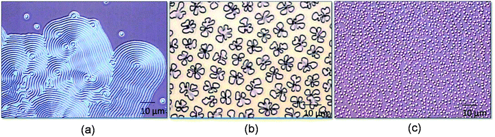 |
| | Fig. 2 Some unexpected and special features resulted from TDL. (a) The pattern looks like a cloud, local parallel stripes and partial concentric circles, observed in the polymer film which are mechanically confined under a compressive stress, like NIL. (b) and (c) show the characteristic flowers and pillars patterns, which are called viscous fingers, and are drawn from the featureless margin of the mask during TDL. | |
 |
| | Fig. 3
Optical micrograph of the self-assembled PS grooves with line width ∼500 nm uniformly stretching for a large area, produced by the TDL method (on the ITO substrate). | |
2.2 Observation and investigation of self-assembled polymer grooves
In our experiments, we perform TDL without any external electric field. This method can be used for both ITO glass and silicon substrates. The morphology of TDL polymer grooves was investigated by AFM as shown in Fig. 4. Fig. 4(a) shows the polymer grooves on the ITO substrate (b) and shows the silicon substrate (the widths of two images are both 20 μm). The thickness (∼85 nm) of the polymer film casting on the silicon substrate is thinner than that (∼120 nm) of the ITO substrate. Obeying the conservation of mass, the slight variation of film thickness, which influences the polymer quantity is enough or not would affect the width of the rising part of grooves. The same influence would occur in different spacer gaps. On the other hand, the heating time determines the completion and perfection of the polymer grooves. Generally, the baking time is around 1 h for a 100 nm spacer gap. As shown in Fig. 5 (a), the cross-sectional image is the middle and instability situation of the process in which the baking time is less than 1 h, then soon cooled and fixed its formation. Though the height of the spacer is ∼100 nm, the height of the induced grooves is only ∼60 nm. The effect of the heating time is collated and shown in Table 2. The sample of Table 2 is the polymer-casts ITO substrate with a 100 nm spacer gap at a baking temperature of 150 °C. We have found that the formation is not exactly linear. And when the baking time is below 30 min, the height of polymer formation is often low or nonexistent. With a lower heating temperature or higher spacer gap than the sample in Table 2, the heating time would be increased to achieve the saturated height of polymer grooves, consistent with the spacer gap. The mechanism of TDL is illustrated in Fig. 6. The charges accumulating at the corner on the upper grating attract the image charges in the melting polymer and cause two peaks on polymer grooves. These unexpected results coincide with the ICE model. Fig. 5(b) is the sample heated for 1 h with completely flat tops which result from the contact with the upper silicon mask. The height of grooves is ∼100 nm which is in line with the spacer's height. A larger gap would require much more time to draw the polymer grooves, but this may not work as the spacer is too high. As the positive and negative charges are further away, the weakened electrostatics force is not large enough to compete with gravity and the polymer's surface tension.
 |
| | Fig. 4 The morphology of TDL polymer grooves was investigated by AFM (the widths of two images are both 20 μm). (a) Polymer grooves with 500 nm widths are formed on the ITO substrate. (b) The TDL is also successful on the silicon substrate. | |
 |
| | Fig. 5 (a) The cross-sectional image shows the middle and instability situation of the process where the baking time is less than 1 h, then soon cooled and fixed its formation. Though the height of the spacer is ∼100 nm, the height of the induced grooves is only ∼60 nm. (b) The sample is heated for 1 h to give a completely flat tops which results from the contact with the upper silicon mask. The height of grooves is ∼100 nm which is consistent with the spacer's height. | |
Table 2 The effect of heating time for TDL. The sample in Table 2 is the polymer-cast ITO substrate with a 100 nm spacer gap at a baking temperature of 150 °C
| Heating time |
30 min |
45 min |
60 min |
>60 min |
| The height of polymer grooves |
∼60 nm |
∼75 nm |
∼100 nm |
∼100 nm |
| Structure morphology |
Not complete |
Not complete |
Complete |
adjacencies merge occasionally |
 |
| | Fig. 6 The illustration represents the ICE model with the charges accumulating at the corner on the upper grating attracting the image charges in the melting polymer, causing the two peaks on the polymer grooves. (As shown in Fig. 5(a).) | |
2.3 Fabrication and measurements of the liquid crystal cells
In the following, we utilized a silicon substrate and an ITO glass with TDL polymer grooves as the bottom substrates to fabricate the reflective and transmissive LC cells, respectively. The bottom substrates were then covered by a conventional indium-tin-oxide (ITO) glass coated with PI planar alignment layers as the upper substrates. The direction of the TDL grooves was set orthogonal to the PI rubbing direction on the opposite substrate. Then, we filled this empty cell with a 4′-n-pentyl-4-cyanobiphenyl (5CB) LCs at room temperature with a cell gap of 4 μm. Therefore, the director configuration of LC sandwiched between the substrate with TDL grooves and the rubbed PI layer becomes twisted by 90° and we fabricated the mixed-mode twisted nematic (MTN) reflective cell and the TN transmissive cell.24,25 The cells are inspected by a polarizing optical microscope and the polarizer setting is required to obtain maximum darkness (or brightness) with zero voltage for the LC cell. Thus, the LC cell belongs to the normally black state (or normally white state). Fig. 7(a) is the normally black mode of the MTN reflective LC cell (period ∼1000 nm, height ∼50 nm) observed under an optical microscope. Applying the voltage between the ITO layer and the p-type silicon substrate, the patterned LC cell, i.e. normally black mode, changed its phase retardation and became bright as seen in Fig. 7(b). Fig. 7(c) shows the 3-dimensional morphology of the polymer grooves on the silicon substrate. Fig. 8 demonstrates the voltage-dependent light transmission (TV curve) of the transmissive TN–LC cell (the insets are the AFM image and optical micrographs). The threshold voltage where the LCs started to change their phase retardation is around 1.3 V. As the applied voltage increased, the LCs orient along the electric field which results in the cell being in the dark state between two crossed polarizers. The response time of this MTN cell was determined to be around 9 ms. These LC cells are quite durable and stable for maintaining their electro–optical properties during weeks of measurements. Based on Berreman's theory, the anchoring energy resulted from grooves is W = 2π3KA2/λ3, where A is the amplitude, λ is the period of the groove and K is the Frank elastic constant of the LC (K5CB = 2 × 10⁻¹² N).26 For the TN–LC cell in Fig. 8, where the period is ∼800 nm and the amplitude is ∼100 nm, the anchoring energy W is ∼0.24 × 10⁻⁵ N m−1. The anchoring energy of conventional PI rubbing is ∼10−5 N m−1 and for AFM rubbing is ∼10−6 N m−1.27,28 Thus, the anchoring energy of TDL polymer grooves between PI rubbing and AFM rubbing is enough to give a good control of LC molecules. The opto-electric performance was good, comparable, and could be improved if a mask with a smaller-period grating was used.
 |
| | Fig. 7 (a) and (b) are optical images. (a) The normally black mode of the MTN reflective LC cell (the period ∼1000 nm, the height ∼50 nm). (b) Applying the voltage between the ITO layer and the p-type silicon substrate, the LC cell entered the bright state. (c) The 3-dimensional morphology of polymer grooves on the silicon substrate. | |
 |
| | Fig. 8 The voltage-dependent light transmission (TV curve) of the transmissive TN–LC cell (the insets are the AFM image and optical micrographs). The threshold voltage of this TV curve is around 1.3 V. As the applied voltage increased, the LCs orient along the electric field which results in the cell being in the dark state when viewed through two crossed polarizers. | |
3. Conclusions
We successfully form periodic self-assembled polymer grooves via thermal drawing lithography route. We have also discovered some interesting results during the experimental process which could be explained by the ICE model. The TDL polymer grooves are utilized to align LC molecules and used as an alignment layer for LC cells whose opto-electric properties are well-performed and comparable to the results of other research groups looking to align LCs. TDL is a low cost, low temperature process and it does not have residual static electricity and dust contamination. It also avoids some of the disadvantages of conventional PI rubbing. In addition to fabricating grating patterns, TDL could be used to create many intriguing micro- or nano-features and their scale can be manipulated via the use of a patterned mask or a totally flat mask. Importantly, TDL is a simple and feasible means to fabricate nanostructures which could be applied to many other fields, not just LC displays, such as biosensors and opto-electric devices.
Acknowledgements
One of us, CYC, would likes to acknowledge the support from the National Science Council and Ministry of Education of the Republic of China.
References
- G. M. Whitesides, E. Ostuni, S. Takayama, X. Jiang and D. E. Ingber, Annu. Rev. Biomed. Eng., 2001, 3, 335 CrossRef CAS.
- P. L. Burn, A. B. Holmes, A. Kraft, D. D. C. Bradley, A. R. Brown, R. H. Friend and R. W. Gymer, Nature, 1992, 356, 47 CrossRef CAS.
- D. M. Tennant, T. L. Koch, P. P. Mulgrew, R. P. Gnall, F. Ostermeyer and J.-M. Verdiell, J. Vac. Sci. Technol., B, 1992, 10, 2530 CrossRef CAS.
- J. H. Kim, M. Yoneya and H. Yokoyama, Nature, 2002, 420, 159 CrossRef CAS.
- D. E. Angelescu, J. H. Waller, D. H. Adamson, P. Deshpande, S. Y. Chou, R. A. Register and P. M. Chaikin, Adv. Mater., 2004, 16, 1736 CrossRef CAS.
- R. Jackman, J. Wilbur and G. M. Whitesides, Science, 1995, 269, 664 CAS.
- M. Böltau, S. Walheim, J. Mlynek, G. Krausch and U. Steiner, Nature, 1998, 391, 877 CrossRef CAS.
- S. Y. Chou, P. R. Krauss and P. J. Renstrom, J. Vac. Sci. Technol., B, 1996, 14, 4129 CrossRef CAS.
- S. Y. Chou and L. Zhuang, J. Vac. Sci. Technol., B, 1999, 17, 3197 CrossRef.
- S. Y. Chou, L. Zhuang and L. Guo, Appl. Phys. Lett., 1999, 75, 1004 CrossRef CAS.
- E. Schäffer, T. Thurn-Albrecht, T. P. Russel and U. Steiner, Nature, 2000, 403, 874 CrossRef CAS.
- F. C. Frank, Discuss. Faraday Soc., 1958, 25, 19 RSC.
- M. Cavallini and F. Biscarini, Nano Lett., 2003, 3, 1269 CrossRef CAS.
- M. Cavallini, C. Albonetti and F. Biscarini, Adv. Mater., 2009, 21, 1043 CrossRef CAS.
- M. Cavallini, A. Caló, P. Stoliar, J. C. Kengne, S. Martins, F. C. Matacotta, F. Quist, G. Gbabode, N. Dumont, Y. H. Geerts and F. Biscarini, Adv. Mater., 2009, 46, 4688.
- S. F. Lyuksyutov, R. A. Vaia, P. B. Paramonov, S. Juhl, L. Waterhouse, R. M. Ralich, G. Sigalov and E. Sancaktar, Nat. Mater., 2003, 2, 468 CrossRef CAS.
- Y. Xia, M. Mrksich, E. Kim and G. M. Whitesides, J. Am. Chem. Soc., 1995, 117, 9576 CrossRef CAS.
- R. Service, Science, 1997, 278, 383 CrossRef CAS.
- H. A. Stone, A. D. Stroock and A. Ajdari, Annu. Rev. Fluid Mech., 2004, 36, 381 CrossRef.
- K. Mizoguchi and E. Hasegawa, Polym. Adv. Technol., 1996, 7, 471 CrossRef CAS.
- J. Peng, Y. Han, Y. Yang and B. Li, Polymer, 2003, 44, 2379 CrossRef CAS.
- A. Lindner, P. Coussot and D. Bonn, Phys. Rev. Lett., 2000, 85, 314 CrossRef CAS.
-
P. A. Deshpande, Ph.D Dissertation Princeton University, 2005.
-
S. T. Wu, D. K. Yang, Reflective Liquid Crystal Displays, ed. A. C. Lowe, Wiley-SID, UK 2001, p. 89–108 Search PubMed.
-
P. Yeh, C. Gu, Optics of Liquid Crystal Displays, ed. J. W. Goodman, John Wiley & Sons, Inc., US 1999, p. 123–124 Search PubMed.
- D. W. Berreman, Phys. Rev. Lett., 1972, 28, 1683 CrossRef CAS.
- H. Yokoyama, Mol. Cryst. Liq. Cryst., 1988, 165, 265 CAS.
- J. H. Kim, M. Yoneya, J. Yamamoto and H. Yokoyama, Nanotechnology, 2002, 13, 133 CrossRef.
|
| This journal is © The Royal Society of Chemistry 2011 |
Click here to see how this site uses Cookies. View our privacy policy here.