The interaction of halogen molecules with SWNTs and graphene†
Sandeep
Ghosh
ab,
S R K C Sharma
Yamijala
a,
Swapan K.
Pati
*de and
C.N.R.
Rao
abc
aChemistry and Physics of Materials Unit, Jawaharlal Nehru Centre for Advanced Scientific Research, Jakkur P.O., Bangalore-560064, India
bSolid State and Structural Chemistry Unit, Indian Institute of Science, Bangalore-560012, India
cInternational Centre for Materials Science, Jawaharlal Nehru Centre for Advanced Scientific Research, Jakkur P.O., Bangalore-560064, India
dTheoretical sciences unit, Jawaharlal Nehru Centre for Advanced Scientific Research, Jakkur P.O., Bangalore-560064, India
eNew Chemistry Unit, Jawaharlal Nehru Centre for Advanced Scientific Research, Jakkur P.O., Bangalore-560064, India. E-mail: pati@jncasr.ac.in; Fax: 91 (80) 2208 2766/2767
First published on 14th December 2011
Abstract
The interaction of halogen molecules of varying electron affinity, such as iodine monochloride (ICl), bromine (Br2), iodine monobromide (IBr) and iodine (I2) with single-walled carbon nanotubes (SWNTs) and graphene has been investigated in detail. Halogen doping of the two nanocarbons has been examined using Raman spectroscopy in conjunction with electronic absorption spectroscopy and extensive theoretical calculations. The halogen molecules, being electron withdrawing in nature, induce distinct changes in the electronic states of both the SWNTs and graphene, which manifests with a change in the spectroscopic signatures. Stiffening of the Raman G-bands of the nanocarbons upon treatment with the different halogen molecules and the emergence of new bands in the electronic absorption spectra, both point to the fact that the halogen molecules are involved in molecular charge-transfer with the nanocarbons. The experimental findings have been explained through density functional theory (DFT) calculations, which suggest that the extent of charge-transfer depends on the electron affinities of the different halogens, which determines the overall spectroscopic properties. The magnitude of the molecular charge-transfer between the halogens and the nanocarbons generally varies in the order ICl > Br2 > IBr > I2, which is consistent with the expected order of electron affinities.
Introduction
Nanomaterials based on carbon, such as single walled carbon nanotubes (SWNTs) and graphene have emerged as exciting materials owing to their interesting properties, the most important ones being related to their electronic structure.1,2 These properties of SWNTs and graphene can lead to many potential applications,3,4 specially in electronic devices.5,6 The ability to tune the Fermi level in these materials by selectively filling or depleting their density of states (DOS) therefore becomes relevant, if device applications are to become a reality. Molecular and electrochemical doping provides a possible method of tuning the electronic structure of SWNTs and graphene7 and the doping level is readily probed by Raman spectroscopy, which is useful to examine changes in electronic structure because of the strong electron–phonon interactions in these materials.7–10 Raman spectroscopy is also a non-invasive technique and can be used in conjunction with other experimental methods. The changes in the electronic band structure of SWNTs and graphene can also be monitored by employing electronic absorption spectroscopy, which gives useful, statistically averaged data.11,12 Such changes can be understood microscopically through theoretical calculations.Doping SWNTs is amphoteric as can be seen from the various reports in the literature on the interaction of SWNTs with various electron donor and acceptor molecules. SWNTs can exchange electrons from the dopants irrespective of whether they are electron donating or withdrawing in nature. Thus, an electron-donating molecule, such as tetrathiafulvalene (TTF) causes changes in the spectroscopic signatures opposite to those due to an electron-withdrawing molecule, such as tetracyanoethylene (TCNE).13 The S22 band in the electronic absorption spectrum of SWNTs13 shifts to higher energy on interaction with TCNE, compared to that of undoped SWNTs, while the shift is in the opposite direction in the case of TTF (i.e. S22 band shifts to lower energy). The Raman spectrum of SWNTs is markedly affected on interaction with these molecules. Coulombic charge-transfer from metals like gold and platinum to SWNTs also induce significant changes in the Raman spectra of the SWNTs, especially the G-band (∼1567 cm−1), which means that the Raman frequency shifts are associated with the shifts in the Fermi level of the SWNTs.14 Similar charge-transfer has been found to occur in the case of metal nanocluster decorated graphene.15 Studies on the interaction of electron donor and acceptor molecules with graphene have demonstrated similar changes in the Raman spectrum of graphene wherein electron donor molecules, such as aniline and TTF softens the G-band.14 Nitrobenzene and TCNE, on the other hand, strengthen the G-band,16 a behaviour similar to that of SWNTs. These experimental observations on molecular doping of graphene and SWNT have been complemented by theoretical studies.17,18
Halogens, such as I2, have traditionally been used as electron withdrawing species to examine their interaction with aromatic molecules.19–21 Therefore it is of interest to study the interaction of different halogen molecules with extended π-systems like SWNTs and graphene by employing Raman and electronic absorption spectroscopy. There are some reports in the literature on the chemical doping of SWNTs by I2 and Br2 ,22,23 but the spectroscopic changes associated with the accompanying charge-transfer interaction have not been properly delineated or explained. Interaction of single layer and bilayer graphenes with I2 and Br2 have been reported recently,24 even though graphite intercalation compounds of halogens have been studied extensively.25
In this article, we describe results of our detailed studies on the interaction of SWNTs and few-layer graphene (FLG) with different halogen molecules probed by spectroscopic methods as well as by first-principles calculations. As-prepared SWNTs produced by the arc-discharge method were subjected to interactions with four halogen molecules namely ICl, Br2, IBr and I2, which would have different electron affinities, the expected order being ICl > Br2 > IBr > I2, based on electronegativity considerations (experimental electron affinities available in the literature do not show any definitive trend26,27). The halogens are expected to p-dope SWNTs to varying degrees. The halogen-doped samples were characterized using Raman and electronic absorption spectroscopy. FLG prepared by the exfoliation of graphite oxide and arc-discharge methods were also interacted with the halogens and the samples studied by spectroscopic methods. The changes in the spectroscopic signatures of both these nanocarbons were found to depend on the level of doping and also on the varying electron-withdrawing ability of the halogens. These experimental findings have been rationalized by DFT investigations.
Results and discussion
SWNTs
Halogen doping causes pronounced changes in the DOS near the Fermi level of the SWNTs as verified by the changes in the Raman spectra of the doped samples in comparison to those of pristine SWNTs. Fig. 1(a) shows the variation in the Raman G-band of iodine monochloride (ICl) doped SWNTs in comparison to that of the as-synthesized sample. As the concentration of ICl in the doped sample is increased, the G-band of the SWNTs shifts to higher wavenumbers. The upshifts in the Raman G-band demonstrate the occurrence of p-doping of the nanotubes by the halogen molecule. | ||
| Fig. 1 Changes in the G-band Raman spectra of (a) SWNT, and (b) graphene as the concentration of doping with ICl is varied. | ||
G-band in graphene, which arises due to the in-plane transverse optical (iTO) phonon mode splits for the nanotube depending on its chirality.28 The G-bands of semiconducting tubes split into two components and are categorised as G+ (∼1590 cm−1, the higher wavenumber component) and G− (∼1567 cm−1, the lower wavenumber component) due to the longitudinal optical (LO - axial) and transverse optical (TO - circumferential) modes, respectively. The TO mode in metallic nanotubes, on the other hand, appears at a higher frequency (G+, ∼1580 cm−1) while the LO mode appears at a lower frequency (G− ∼1540 cm−1), in comparison to the semiconducting nanotubes.7 The positions of the G-bands depends upon various factors, such as extent of bundling, environment, synthetic procedure etc. and hence the band positions mentioned above vary to some degree. The maximum in the composite G-band is mainly due to the LO mode of the semiconducting tubes while the shoulder around 1540 cm−1 mostly arises from the LO mode of the metallic tubes. As the ICl content in the doped sample is increased (see Fig. 1(a)), there is a progressive decrease in the intensity of the 1540 cm−1 feature relative to the G-band maximum, indicating that the metallic SWNTs get converted to semiconducting ones due to changes in the DOS near the Fermi level.
The extent of G-band shifts varies with the magnitude of doping and the halogen molecule as illustrated in Fig. 2, which shows the variation of the G-band frequency as a function of the amount of different halogens used to dope a mole of SWNTs. The strengthening of the G-band follows the general order of I2 < IBr < Br2 < ICl, which is consistent with the expected order of electron affinities of the halogen molecules. The G-band shifts for the same C![[thin space (1/6-em)]](https://www.rsc.org/images/entities/char_2009.gif) :X2 molar ratio (10:1) for different halogens are plotted in Fig. 3 to present this trend more clearly. As can be inferred from Fig. 3, the higher the electron affinity of the halogen molecule (ICl in the present case) the higher the G-band shift from that of the pure SWNT.
:X2 molar ratio (10:1) for different halogens are plotted in Fig. 3 to present this trend more clearly. As can be inferred from Fig. 3, the higher the electron affinity of the halogen molecule (ICl in the present case) the higher the G-band shift from that of the pure SWNT.
 | ||
| Fig. 2 Changes in the G-band position (LO mode of semiconducting nanotubes) for doping a mole of SWNTs with different halogens. | ||
 | ||
| Fig. 3 Changes in the Raman signatures in SWNTs for doping with different halogens (for doping molar ratio of 10:1 halogen:carbon). | ||
The conversion of metallic SWNTs into semiconducting ones becomes even more apparent when the composite G-bands of the doped nanotubes are decomposed into individual metallic and semiconducting components. The ratio of the intensities of the LO mode of the metallic species to that of the semiconducting nanotube in the Raman spectra of the doped samples is plotted in Fig. 4 as a function of the halogen doping level in the case of ICl and Br2. In the case of halogen molecules with relatively higher electron affinities, such as Br2 and ICl, the reduction in the Raman signal of the metallic G-bands is highly pronounced as can be deduced from Fig. 4. This implies that these two halogen molecules convert metallic SWNTs into semiconducting ones (ICl having the better capability). The changes in the relative intensities of the metallic vs. semiconducting LO modes for all the halogen molecules lead us to the following order of metallic to semiconducting conversion: ICl > Br2 > IBr ≈ I2.
 | ||
| Fig. 4 Variation of the intensity ratios of Raman LO modes of metallic vs. semiconducting SWNTs for different doping levels of bromine and ICl. | ||
Graphene
Typical G-band Raman shifts associated with halogen doping of FLG are shown in Fig. 1(b). The G-band in graphene is composed of essentially two components namely a G-band (which has the same origin as that mentioned earlier) and a D-band (which is associated with defects in the graphene crystal lattice) that appears as a shoulder on the higher wavenumber side of the G-band. The strengthening of the G-band increases with ICl content in the doped graphene sample but not as much as in the case of the SWNTs. The G-band of FLG does not show a marked change on doping with different halogens as in the case of SWNTs, as can be seen from Fig. 5(a) wherein the Raman G-band shifts are plotted against the doping level (per mole of FLG) of the different halogens. The changes are, by and large, within the uncertainty of the measurements. If we take the observed small shifts of FLG in Fig. 5(a) seriously, the effect of the different halogen molecules of graphene turns out to be opposite to that observed in the case of SWNTs, but the difference in the shifts are so small that we cannot be certain about this trend. The full-width at half-maximum (FWHM) of the halogen-doped graphene samples also do not show much variation with the halogen (see inset of Fig. 5(a)). The increase in the D-band intensity suggests that doping FLG induces more defects. | ||
| Fig. 5 (a) G-band characteristics for graphene (inset shows the variation in FWHM) for various amounts of different halogens for a fixed molar amount of graphene (1 mol). (b) 2D band characteristics for graphene as the concentration of bromine doping is varied. | ||
Fig. 5(b) illustrates the variation of the 2D band intensity on doping FLG with Br2. We see that the intensity of the 2D band decreases markedly as the Br2 content is increased. It should be noted that the ratio of intensities of the 2D band and the G-band is extremely sensitive to doping by either holes or electrons. We find that the decrease in the I2D/IG ratio (for a C:X2 ratio of 1:2.8) is maximum for ICl and minimum for I2. The magnitude of the decrease in the intensity of the 2D band by the different halogen molecules is the same as observed in case of the G-band for SWNTs (ICl > Br2 > IBr > I2).
It is worthwhile to note in this connection that the Raman spectra of doped samples of both SWNTs and graphene can be regenerated to that of the pristine samples by simply heating out the halogen at elevated temperatures.
Doping in graphene is further confirmed from electronic absorption spectroscopy, which showed noticeable changes. Fig. 6 shows the variation in the electronic absorption spectrum of a EG–I2 charge-transfer complex (C:X2 molar ratio 1:2.8) as the amount of iodine in the doped sample is varied. Electronic absorption spectrum due to pristine graphene exhibits a band centred around 240 nm, which originates due to the π–π* transition near the M-point of the two-dimensional Brillouin zone of graphene.29,30 Iodine doping of EG leads to the complete disappearance of this band and the emergence of two new bands centred around 215 nm and 280 nm. The two new bands can be associated with the charge-transfer interaction between EG and iodine as these bands disappear on removal of iodine (by heating) from the doped sample as illustrated in Fig. 6. The band at 215 nm shifted to higher energy while the band at 280 nm simply reduced in intensity accompanied by the slow regeneration of the π-plasmon band of pristine graphene.
 | ||
| Fig. 6 Changes in the electronic absorption spectra of the EG–I2 complex of molar ratio 1:2.8 (carbon:halogen) as the iodine is slowly removed, compared with the spectrum of pristine exfoliated graphene. | ||
Similar changes in the electronic absorption spectra of doped SWNT samples were observed in addition to changes in the inter-van Hove transitions M11, S11 and S22. The π-plasmon band of pristine graphene splits into two in the case of SWNTs and these bands show significant polarization dependence,31 in addition to being dependent on solvent and nanotube bundling. The changes in the halogen doping induces remarkable changes in the π-plasmon bands of SWNTs as shown in Fig. 7(a). The π-plasmon bands originally centred around 227 nm and 270 nm were replaced by a set of bands centred around 240 nm and 280 nm upon doping, and their position did not change on heating out the bromine and instead increased in intensity (see Fig. 8(a)). The changes in the band positions can be attributed to the charge-transfer interaction between the SWNTs and bromine. However, since halogen doping induces debundling of the SWNTs, thereby decreasing the interaction between neighbouring tubes,32 the π-plasmon bands do not revert back to their original positions. The effect of doping on the inter-van Hove transitions of SWNTs is shown in Fig. 7(b). Doping the SWNTs with bromine led to the disappearance of the M11 (∼720 nm), S22 (∼1050 nm) and S11 (∼1870 nm) bands accompanied by the emergence of a new band at ∼950 nm. The electronic absorption spectrum of the bromine doped sample in the region of inter-van Hove transitions could be restored upon heating out the bromine. The other halogen molecules caused similar changes in the electronic absorption spectrum of the nanotubes.
 | ||
| Fig. 7 Changes in the electronic absorption spectra of the SWNT–Br2 complex of molar ratio 20:1 (carbon:halogen) as the Br2 is slowly removed in comparison to the spectrum of pristine SWNTs. | ||
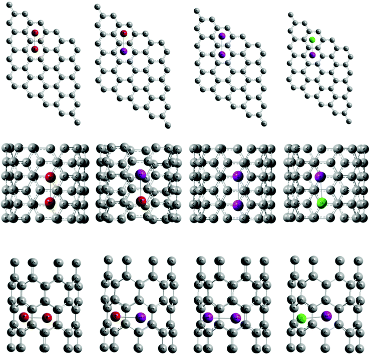 | ||
| Fig. 8 Optimized halogen adsorbed nanocarbons. From Top to bottom graphene, CNT (5, 5), CNT (8, 0), respectively and from left to right Br2, IBr, I2, ICl adsorbed nanocarbons, respectively. | ||
For a microscopic understanding of these experimental results, we have performed DFT computations on the various halogen–nanocarbon complexes. The details of the calculations are provided in the computational methods. In the case of SWNTs, the theoretical studies were performed on model metallic (5,5) and semiconducting (8,0) nanotubes. Adsorption energies of the different halogen–nanocarbon complexes were calculated to understand their relative stability. The adsorption energy per adsorbate molecule is calculated as the energy difference between the optimized total energy of the halogen–nanocarbon complex and the individual energies of the halogen molecule and the pristine nanocarbon.
| E (adsorption) = E (halogen–nanocarbon complex) −E (halogen molecule) − E (pristine nanocarbon) | (1) |
The various adsorption parameters concerning the different halogen–nanocarbon systems viz. adsorption energies and equilibrium distances of separation between nanocarbons and adsorbed halogens are presented in Table 1 and the corresponding optimized structures are shown in Fig. 8. The stronger the interaction between the halogens and the nanocarbons, the greater will be the adsorption energy of the complex. Hence, as is evident from Table 1, all the adsorption energy values are in the range of ∼1–2 eV (23–46 kcal mol−1), which clearly indicates that the halogen molecules are physisorbed on nanocarbon surfaces, the equilibrium distances of adsorption being of the order of ∼2.8 Å to ∼3.3 Å. It can also be envisaged from Table 1 that the order of adsorption energy is the same for all the halogen molecules (for both the nanocarbons), Br2 being the strongest adsorbate and ICl being the weakest. To identify the feasible reason for the general order of halogen–nanocarbon interaction energies (i.e. Br2 > IBr > I2 > ICl according to Table 1), the adiabatic electron affinities of the various halogen molecules were calculated using the same level of theory as mentioned earlier. The order of electron affinities is found to be the same as the order of interaction energies i.e. Br2 > IBr > I2 > ICl, leading us to conclude that the higher the electron affinity of the halogen the greater will be its interaction with the nanocarbon. Interestingly, the adsorption energies of all the halogens to the nanocarbons follows the order CNT (5, 5) > Graphene > CNT (8, 0). This indicates that the extent of interaction of a halogen with the nanocarbons (only for those considered here) increases in the order semiconducting < semi-metallic < metallic i.e. in the order of abundance of electrons in the nanocarbon. Thus, from the order of adsorption energies of the halogens with different nanocarbons, we find that, molecules with higher electron affinities interact strongly with the electron rich nanocarbons. From Mülliken population analysis, we find that the extent of charge-transfer is relatively small (only ∼0.2% charge-transfer is observed) in order to draw a comparison for the observed trends. Note that, the Mülliken population analysis is highly basis set dependent, and only gives a qualitative picture of charge-transfer. We also calculated the first ionization energies of all the molecules using the same level of theory, to compare the electron donating capability of the molecules and we find that the electron donating order is I2 > IBr > Br2 > ICl.
| CNT (5, 5) | Graphene | CNT (8, 0) | |||||||
|---|---|---|---|---|---|---|---|---|---|
| Molecule | Equilibrium distance (Å) | Adsorption energy (eV) | Band gap (eV) | Equilibrium distance (Å) | Adsorption energy (eV) | Band gap (eV) | Equilibrium distance (Å) | Adsorption energy (eV) | Band gap (eV) |
| Br2 | 3.03 | −2.00 | 0.05 | 2.81 | −1.88 | 0.27 | 2.82 | −1.87 | 0.32 |
| IBr | 3.07 | −1.82 | 0.02 | 3.06 | −1.71 | 0.19 | 2.83 | −1.70 | 0.30 |
| I2 | 3.27 | −1.09 | 0 | 3.05 | −1.52 | 0.09 | 3.05 | −1.54 | 0.28 |
| ICl | 3.18 | −1.10 | 0 | 3.09 | −1.01 | 0.32 | 3.16 | −0.98 | 0 |
| Pristine | — | — | 0 | — | — | 0 | — | — | 0.41 |
To understand the effect of halogen adsorption on the electronic properties of nanocarbons, the band diagrams and the corresponding density of states (DOS) were plotted together with the projected DOS (PDOS) for all the systems as shown in Fig. S1, S2, S3 (ESI†) for graphene, CNT (5, 5) and CNT (8, 0), respectively. Halogen adsorption significantly changes the DOS of graphene (Fig. S1, ESI†) near the Fermi energy, whereas, for the case of CNT (8, 0) and CNT (5, 5) changes are comparatively smaller (Fig. S2, S3, ESI†). We also find that the energy band gap of nanocarbons changes upon halogen adsorption and the changes follow the same order as the electron affinity of the halogen molecules for SWNTs (i.e. Br2 > IBr > I2 > ICl) and for graphene it follows the ionization energy order. The calculated band gap of each halogen adsorbed nanocarbon is reported in Table 1. Moreover, the linear band dispersion behavior at the Fermi level in pristine graphene is destroyed with a generation of energy band gap (in the order of ∼0.088–0.27 eV) at the Fermi level after the adsorption of molecular species. Near the Fermi level there are discrete molecular bands which are essentially a superposition of bands from both the graphene and that of the adsorbate, with a larger contribution from adsorbed molecules, as can be seen from the DOS and PDOS of the complexes (Fig. S1, ESI†). In the case of SWNTs (i. e. for both (8, 0) and (5, 5)), there is a change in the band structure near the Fermi level (see Fig. S3 and S2, ESI†) due to the presence of adsorbed molecules, which is not as pronounced in the case of graphene. Compared to the pristine semiconducting SWNT (8, 0), some extra bands were found to originate slightly below the Fermi level. These energy levels arise from the adsorbed molecules as illustrated in the projected density of states of these particular complexes. Band structure for the halogen adsorbed SWNT (5, 5), however, does not change much near the Fermi level.
The Fermi energy shifts for the nanocarbons upon halogen adsorption follow exactly the same trend for both the nanocarbons viz. I2 > IBr > Br2 > ICl, which is in accordance with the electron donating capability of the halogen species. This can be explained on the basis of the fact that as the electrons are added to the conduction band, there should be an upward shift in the Fermi energy. I2 has less ionization energy (or more electron donating capability) and hence the Fermi energy shifts towards the conduction band, and this shift is larger compared to other halogen adsorbed systems because of its higher electron donating capability. The order of the shifts in the Fermi energy for other molecules can be explained in a similar manner. It is well known that greater the amount of charge transferred to/from the nanocarbon the greater the softening/strengthening of the G-band.7,14,16,17,22,24,33–35 In accordance with the above argument for the order of Fermi energy shift, iodine should strengthen the G-band less as compared to others and iodine monochloride should strengthen the G-band more and the order should be ICl > Br2 > IBr > I2, which qualitatively matches the experimental G-band shift for SWNTs. The electron affinity order obtained for these molecules, supports the above shift in G-band order (except for ICl). The electron affinity order obtained from theoretical calculations is Br2 > IBr > I2 > ICl and the experimental G-band stiffening varies in the order ICl > Br2 > IBr > I2. Thus, the order of electron affinity matches with that experimental G-band strengthening.
Interestingly, for both CNT (8,0) and CNT (5,5) ICl adsorption leads to a finite DOS at the Fermi level. From the PDOS of ICl adsorbed CNT (5,5) (Fig. S2, ESI†) one can notice that there is a significant contribution from the iodine and chlorine atoms to the DOS at the Femi energy for this complex, thus resulting in metallic behavior. Unlikely, for the case of CNT (8, 0) the contribution to the DOS at the Fermi energy mainly comes from the carbon atoms. The reason for the metallicity could be as a result of the structural distortion and the presence of the DOS of adsorbate or of carbon at the Fermi energy, rather than the charge-transfer, because the change in the charge of the nanocarbons is too insignificant to account for such a huge change in band structure.
Conclusions
In conclusion, doping by molecular charge-transfer induced by the interaction of different halogen molecules with SWNTs and few-layer graphene has been investigated by employing Raman spectroscopy, electronic absorption spectroscopy and theoretical studies. The spectroscopic signature of doping is more pronounced in the case of SWNTs compared to graphene. The varying electron withdrawing ability of the different halogens (manifested by their electron affinity) produces differences in the spectral properties of the doped samples of both SWNTs and graphene. On average, the observed changes in the Raman spectra of SWNTs and graphene brought about by the halogens conforms to the order, ICl > Br2 > IBr > I2. The trend is what one would expect on the basis of electronegativities of the halogens. Unfortunately, literature data on electron affinities of halogens are not available from the same source. The regeneration of the spectra of the doped samples, after heating, points to the fact that the halogen molecules were adsorbed on the nanocarbon surface without causing any considerable damage to the π-electron system of SWNTs or graphene. The theoretical calculations support the conclusions from the experimental studies.Experimental
Preparation of SWNTs and FLG
SWNTs, prepared by the traditional arc-discharge technique using Y2O3 + Ni , were purified by successive acid and hydrogen treatments and used as such.36,37 FLG employed in our experiments were prepared by two methods; by the exfoliation of graphite oxide and the arc-discharge method. Exfoliated graphene (EG) was prepared by the exfoliation of graphite oxide in a furnace preheated to 1050 °C in an inert atmosphere of argon gas for about 30 s as previously reported.38,39 The number of layers in the EG samples is 4 ± 1, as determined from atomic force microscopy and calculated from the (002) reflection in the XRD pattern. FLG employed in our studies were also prepared by the arc-discharge technique (HG), which involves striking an arc between two graphite electrodes under a relatively high pressure of hydrogen and subsequent formation of graphene flakes generally containing 2–4 layers.40Preparation of halogen doped SWNTs and graphene
The halogens employed in our study are ICl, Br2, IBr and I2, which were purchased from Aldrich Chemical Co. Doping the SWNTs and FLGs with the halogens was performed by mixing a pre-calculated ratio of the nanocarbons and the halogens and sealing this mixture in a glass tube under vacuum. The glass tube was then placed in a tube furnace in such a way that the other end of the glass tube (which is the non-sample end) gets heated at 250 °C so that the sample-end remains at a lower temperature of 200 °C owing to the temperature gradient along the tube. This ensures that the vaporized halogens would effectively dope the SWNTs or the FLGs, which are placed at the colder end of the tube. The tubes were heated for 2–3 h to ensure completion of the doping. The molar ratios of carbon:halogen (C:X2) for different halogens were kept constant. In case of SWNTs, three C:X2 molar ratios were investigated, which were 100:1, 20:1 and 10:1 while the C:X2 molar ratios for FLG were 1:0.7, 1:1.4 and 1:2.8.
Spectroscopic investigation of nanocarbon–halogen charge-transfer complex
Raman spectroscopy and electronic absorption spectroscopy were employed to study the various charge-transfer complexes. Raman spectra were recorded with a LabRAM HR800 high resolution Raman spectrometer (Horiba-Jobin Yvon) using a He–Ne laser (λ = 632.8 nm). Raman spectra were recorded on ten different spots on each sample and the average spectrum was analyzed. Electronic absorption spectra were recorded with a Perkin-Elmer Lambda 900 UV/VIS/NIR spectrometer.Computational details
All the electronic structural and energetic calculations were performed using the linear combination of atomic orbital density functional theory (DFT) within the generalized gradient approximation (GGA), considering the Perdew–Burke–Enzerhof (PBE)41 exchange and correlation functional and using the double zeta polarized basis set (DZP) for all atoms as implemented in the SIESTA package.42 Although, it is known that DFT poorly describes dispersion forces for the physisorption of the molecules, the molecules under consideration, owing to their lack of π-surface, render dispersion forces less important and hence the qualitative estimations of the obtained results would not change much. This is evident from the large number of studies involving the same method for gas molecule adsorption in the literature.17,18,43–47 It should also be noted that local density approximation (LDA) overestimates the adsorption energy48 for the weakly bound charge-transfer systems and hence, we believe that GGA is an appropriate choice for our calculations describing the interaction between the halogens and the nanocarbons.We have considered the norm conserving pseudo potentials49 in the fully non-local Kleinman–Bylander form50 and are constructed from 7 valence electrons for all the halogens. A real space mesh cut off of 400 Ryd is used for both graphene and SWNTs. For complete relaxation, a Monkhorst k-point grid of 1 × 1 × 6 and 6 × 6 × 1 were used, respectively for systems involving SWNTs and graphene. Systems are considered to be relaxed when the forces acting on all the atoms are less than 0.04 eV Å−1. For electronic properties, the Brilliouin zone is sampled as 1 × 1 × 20 and 12 × 12 × 1 for systems involving SWNTs and graphene, respectively. The calculations are performed in supercells, chosen such that the interactions between the systems in directions other than the direction in which the system is periodic are negligible. We separately relaxed the structures of pristine graphene (52 atoms) and SWNT (66 and 62 atoms for semiconducting and metallic, respectively), halogen molecules and also halogen–nanocarbon complex supercells at the same level of calculation. The initial structures for the geometry optimization of halogen adsorbed SWNTs are considered by placing the halogen molecules on top of the centers of two adjacent benzene rings of SWNTs, as shown in Fig. 8. We have considered graphene in the xy-plane and to create a sufficient vacuum along the z-direction a translation vector of 25 Å is considered to ensure the energy convergence. In the case of SWNTs, translational vectors of 15 Å are considered along x and y directions to avoid unwanted interactions.
References
- R. Saito, G. Dresselhaus and M. S. Dresselhaus, Physical Properties of Carbon Nanotubes, 1998 Search PubMed.
- A. K. Geim and K. S. Novoselov, Nat. Mater., 2007, 6, 183–191 CrossRef CAS.
- W. Liang, M. Bockrath, D. Bozovic, J. H. Hafner, M. Tinkham and H. Park, Nature, 2001, 411, 665–669 CrossRef CAS.
- M. S. P. Shaffer and A. H. Windle, Adv. Mater., 1999, 11, 937–941 CrossRef CAS.
- H. W. C. Postma, T. Teepen, Z. Yao, M. Grifoni and C. Dekker, Science, 2001, 293, 76–79 CrossRef CAS.
- Y.-M. Lin, C. Dimitrakopoulos, K. A. Jenkins, D. B. Farmer, H.-Y. Chiu, A. Grill and P. Avouris, Science, 2010, 327, 662 CrossRef CAS.
- A. Das, A. K. Sood, A. Govindaraj, A. M. Saitta, M. Lazzeri, F. Mauri and C. N. R. Rao, Phys. Rev. Lett., 2007, 99, 136803 CrossRef.
- M. S. Dresselhaus and P. C. Eklund, Adv. Phys., 2000, 49, 705–814 CrossRef CAS.
- M. Lazzeri, S. Piscanec, F. Mauri, A. C. Ferrari and J. Robertson, Phys. Rev. B, 2006, 73, 155426 CrossRef.
- L. M. Malard, M. A. Pimenta, G. Dresselhaus and M. S. Dresselhaus, Phys. Rep., 2009, 473, 51–87 CrossRef CAS.
- M. E. Itkis, D. E. Perea, S. Niyogi, S. M. Rickard, M. A. Hamon, H. Hu, B. Zhao and R. C. Haddon, Nano Lett., 2003, 3, 309–314 CrossRef CAS.
- B. J. Landi, H. J. Ruf, C. M. Evans, C. D. Cress and R. P. Raffaelle, J. Phys. Chem. B, 2005, 109, 9952–9965 CrossRef CAS.
- R. Voggu, C. S. Rout, A. D. Franklin, T. S. Fisher and C. N. R. Rao, J. Phys. Chem. C, 2008, 112, 13053–13056 CAS.
- R. Voggu, C. S. Rout, A. D. Franklin, T. S. Fisher and C. N. R. Rao, J. Phys. Chem. C, 2008, 112, 13053–13056 CAS.
- K. S. Subrahmanyam, A. K. Manna, S. K. Pati and C. N. R. Rao, Chem. Phys. Lett., 2010, 497, 70–75 CrossRef CAS.
- R. Voggu, B. Das, C. S. Rout and C. N. R. Rao, J. Phys.: Condens. Matter, 2008, 20, 472204 CrossRef.
- A. K. Manna and S. K. Pati, Chem. – Asian J., 2009, 4, 855–860 CrossRef CAS.
- A. K. Manna and S. K. Pati, Nanoscale, 2010, 2, 1190–1195 RSC.
- H. A. Benesi and J. H. Hildebrand, J. Am. Chem. Soc., 1949, 71, 2703–2707 CrossRef CAS.
- C. Reid and R. S. Mulliken, J. Am. Chem. Soc., 1954, 76, 3869–3874 CrossRef CAS.
- C. N. R. Rao, S. N. Bhat and P. C. Dwedi, Appl. Spectrosc. Rev., 1972, 5, 1–170 CrossRef.
- A. M. Rao, P. C. Eklund, S. Bandow, A. Thess and R. E. Smalley, Nature, 1997, 388, 257–259 CrossRef CAS.
- S. Kazaoui, N. Minami, R. Jacquemin, H. Kataura and Y. Achiba, Phys. Rev. B, 1999, 60, 13339–13342 CrossRef CAS.
- N. Jung, N. Kim, S. Jockusch, N. J. Turro, P. Kim and L. Brus, Nano Lett., 2009, 9, 4133–4137 CrossRef CAS.
- M. S. Dresselhaus and G. Dresselhaus, Adv. Phys., 2002, 51, 1–186 CrossRef CAS.
- B. K. Janousek and J. I. Brauman, ed. M. T. Bowers, Academic Press, New York, Editon edn 1979, vol. 2, p. 53.
- K. P. Huber and G. Herzberg, Molecular Spectra and Molecular Structure. IV. Constants of Diatomic Molecules, Van Nostrand Reinhold Co., 1979 Search PubMed.
- M. S. Dresselhaus, G. Dresselhaus, R. Saito and A. Jorio, Phys. Reports, 2005, 409, 47–99 CrossRef.
- E. A. Taft and H. R. Philipp, Phys. Rev., 1965, 138, A197–A202 CrossRef.
- P. E. Trevisanutto, M. Holzmann, M. Cote and V. Olevano, Phys. Rev. B, 2010, 81, 121405 CrossRef.
- Y. Murakami, E. Einarsson, T. Edamura and S. Maruyama, Phys. Rev. Lett., 2005, 94, 087402 CrossRef.
- L. Grigorian, K. A. Williams, S. Fang, G. U. Sumanasekera, A. L. Loper, E. C. Dickey, S. J. Pennycook and P. C. Eklund, Phys. Rev. Lett., 1998, 80, 5560–5563 CrossRef CAS.
- B. Das, R. Voggu, C. S. Rout and C. N. R. Rao, Chem. Commun., 2008, 5155–5157 RSC.
- N. Park, Y. Miyamoto, K. Lee, W. Ih Choi, J. Ihm, J. Yu and S. Han, Chem. Phys. Lett., 2005, 403, 135–139 CrossRef CAS.
- C. Hayakawa, K. Urita, T. Ohba, H. Kanoh and K. Kaneko, Langmuir, 2009, 25, 1795–1799 CrossRef CAS.
- C. Journet, W. K. Maser, P. Bernier, A. Loiseau, M. L. de la Chapelle, S. Lefrant, P. Deniard, R. Lee and J. E. Fischer, Nature, 1997, 388, 756–758 CrossRef CAS.
- S. R. C. Vivekchand, A. Govindaraj, M. M. Seikh and C. N. R. Rao, J. Phys. Chem. B, 2004, 108, 6935–6937 CrossRef CAS.
- H. C. Schniepp, J.-L. Li, M. J. McAllister, H. Sai, M. Herrera-Alonso, D. H. Adamson, R. K. Prud'homme, R. Car, D. A. Saville and I. A. Aksay, J. Phys. Chem. B, 2006, 110, 8535–8539 CrossRef CAS.
- K. S. Subrahmanyam, S. R. C. Vivekchand, A. Govindaraj and C. N. R. Rao, J. Mater. Chem., 2008, 18, 1517–1523 RSC.
- K. S. Subrahmanyam, L. S. Panchakarla, A. Govindaraj and C. N. R. Rao, J. Phys. Chem. C, 2009, 113, 4257–4259 CAS.
- K. Burke, J. P. Perdew and M. Ernzerhof, Int. J. Quantum Chem., 1997, 61, 287–293 CrossRef CAS.
- J. M. Soler, E. Artacho, J. D. Gale, A. Garcia, J. Junquera, P. Ordejon and D. Sanchez-Portal, J. Phys.: Condens. Matter, 2002, 14, 2745 CrossRef CAS.
- Y. Okamoto and Y. Miyamoto, J. Phys. Chem. B, 2001, 105, 3470–3474 CrossRef CAS.
- A. Ferre-Vilaplana, J. Chem. Phys., 2005, 122, 104709–104710 CrossRef CAS.
- A. Ferre-Vilaplana, J. Chem. Phys., 2005, 122, 214724–214727 CrossRef CAS.
- S.-H. Jhi and Y.-K. Kwon, Phys. Rev. B, 2004, 69, 245407 CrossRef.
- A. Datta and S. K. Pati, J. Phys. Chem. C, 2007, 111, 4487–4490 CAS.
- D. R. Salahub, Transition-Metal Atoms and Dimers, John Wiley & Sons, Inc., 1987 Search PubMed.
- N. Troullier and L. M. Jose, Phys. Rev. B, 1991, 43, 1993 CrossRef CAS.
- L. Kleinman and D. M. Bylander, Phys. Rev. Lett., 1982, 48, 1425 CrossRef CAS.
Footnote |
| † Electronic Supplementary Information (ESI) available. See DOI: 10.1039/c1ra00295c/ |
| This journal is © The Royal Society of Chemistry 2012 |