Fabrication of cuprous oxide nanoparticles by laser ablation in PVP aqueous solution
Peisheng
Liu
*ac,
Zhigang
Li
b,
Weiping
Cai
c,
Ming
Fang
c and
Xiangdong
Luo
a
aJiangsu Key Laboratory of ASCI Design, Nantong University, Nantong, 226019, P.R. China. E-mail: psliu@isssp.ac.cn(P.L.)
bDepartment of Physics & Electronic Engineering, Taizhou University, Taizhou, 317000, P. R. China
cKey Laboratory of Materials Physics, Anhui Key Laboratory of Nanomaterials and Nanotechnology, Institute of Solid State Physics, Chinese Academy of Sciences, Hefei, 230031, P. R. China
First published on 2nd September 2011
Abstract
The cuprous oxide nanoparticles have been fabricated through pulsed laser ablation of copper target in PVP aqueous solution. The structure, morphology and composition of the nanoparticles have been characterized by X-ray powder diffraction (XRD), transmission electron microscopy (TEM), high-resolution TEM (HRTEM), X-ray photoelectron spectroscopy (XPS) and X-ray excited auger spectra (XAES). The results show that the mean size of the as-prepared in diameter is about 29 nm with a relative narrow size distribution and samples are polycrystal Cu2O nanoparticles with a shell of thin layer of amorphous CuO. Furthermore, a possible mechanism for formation of such the cuprous oxide nanoparticles is discussed. We concluded that pulsed laser ablation of copper in liquid is a feasible method for the synthesis of cuprous oxide nanoparticles.
1. Introduction
Cuprous oxide (Cu2O), as a small (∼2 eV) direct bandgap p-type semiconductor,1–2 has received great attentions because of its potential applications in solar energy conversion,2,3 photocatalytic degradation of organic pollutants,4–5 photoactivated splitting of water under visible light,6–7 and in lithium ion batteries.8–9Cu2O is a paradigm material for research on Bose-Einstein condensation.10 It is also an ideal compound to study the influence of electron-correlation effects on the electronic structure of transition metal compounds in general, and the high Tc superconductors in particular.11 Moreover, Cu2O is non-toxic, inexpensive and abundant in nature. Because of the unique properties in this material, many different ways have developed to create cuprous oxide. Cuprous oxide can be produced by electrolysis,12–14 thermal oxidation,15 hydrothermal production, reduction of cupric salts16 or copper oxide17 in solution, and by the γ irradiation method.18Chemical vapor deposition,19molecular-beam epitaxy (MBE),20,21 and pulsed Laser deposition (PLD)22 have also been employed to synthesize Cu2O. High temperature, special conditions or tedious procedures are required for these methods.In this article, we report a versatile technique for fabrication of Cu2O nanoparticles at room temperature. This technique is based on liquid ablation processes. Pulsed Laser ablation in liquid is an efficient and widely adopted way to synthesize different nanoparticles.23–29 The advantage of this method is the strong confinement of the expanding plasma produced by laser ablation of a target in solution, which can realize extremely high temperature and high pressure. During Pulsed Laser ablation in liquid, super-high temperature (about 6000 K) and high-pressure (about 1 GPa) will generate on the solid-liquid interface, and quench quickly after one pulse, which leads to a non-equilibrium process.30 It has been shown that Cu2O nanoparticles of size in diameter between 15 nm and 60 nm have been synthesized. X-ray photoelectron spectroscopic studies show the inevitable presence of amorphous CuO on the surface of the polycrystalline Cu2O nanoparticles. The details are reported in this article.
2. Experiments
An electrolytic Copper plate (99.99%, about 2 cm × 2 cm) was first fixed on a bracket in a quartz glass vessel filled with 15 ml 0.1 M poly(vinylpyrrolidone) (PVP K-30, Mw = 40![[thin space (1/6-em)]](https://www.rsc.org/images/entities/char_2009.gif) 000, Aldrich) aqueous solution, which was continuously stirred. The plate was located at 4 mm below the solution surface, and then irradiated for 60 min by the first harmonic of a Nd:YAG pulsed laser (wavelength 1064 nm, frequency 10 Hz, pulse duration 10 ns) with power about 80 mJ/pulse and spot size about 2 mm in diameter on the target. After irradiation, the solutions were centrifuged at 14000 rpm. The obtained powder-products were ultrasonically rinsed with ethanol for several times, intending to remove the surfactant PVP molecules on the particles as much as possible, and then draught-dried at room temperature.
000, Aldrich) aqueous solution, which was continuously stirred. The plate was located at 4 mm below the solution surface, and then irradiated for 60 min by the first harmonic of a Nd:YAG pulsed laser (wavelength 1064 nm, frequency 10 Hz, pulse duration 10 ns) with power about 80 mJ/pulse and spot size about 2 mm in diameter on the target. After irradiation, the solutions were centrifuged at 14000 rpm. The obtained powder-products were ultrasonically rinsed with ethanol for several times, intending to remove the surfactant PVP molecules on the particles as much as possible, and then draught-dried at room temperature.
X-ray diffraction (XRD) (Philips X'Pert using Cu Kα line 0.15419 nm) was measured directly for these powder samples. For transmission electron microscopic (TEM) and high resolution transmission electron microscopic (HRTEM) examination, the powder samples were ultrasonically re-dispersed in ethanol, before it was dropped on the copper grids coated with thin carbon film and evaporated in air at room temperature. TEM and HRTEM observations were conducted on a JEOL 2010 TEM, operating at an accelerating voltage of 200 kV. X-ray photoelectron spectra (XPS) were collected by using a Thermo ESCALab 250 X-ray photoelectron spectrometer from V.G. Scientific at CAE mode. A monochromatic X-ray source of Al Kα (1486.6 eV) of 150 W was used as an excitation source. The Spot Size is 500 μm. In addition, the spectra of Cu Auger electrons excited by X-ray radiation were measured. The binding energies obtained in the XPS analysis were corrected with reference to C1s (284.6 eV). The peak positions and areas were determined by fitting the unsmoothed spectra after subtraction of linear back ground. Curve fitting of over-lapping spectral lines was carried out using the lines of Gaussian–Lorentzian shape and using XPSPEAK4.1 fitting soft ware.
3. Results and discussions
It has been shown that the colloidal solutions are stable without apparent aggregation and the color of the colloidal solution and the powder is dark red (as shown in the inset of Fig. 1). | ||
| Fig. 1 XRD pattern of the as prepared sample .The insert is the picture of as prepared colloidal solution. | ||
3.1 Structure and morphology
Fig. 1 shows an X-ray diffraction (XRD) pattern of the as-prepared Samples. The XRD spectrum contains four peaks that are clearly distinguishable. All of them can be perfectly indexed to crystalline Cu2O. The diffraction peaks are in good agreement with Cu2O powder (JCPSD Card No. 05-0667) with the lattice parameter a = 4.2696 Å. No other characteristic peaks are observed for the other impurities such as Cu and CuO. The crystallite size of the particles was calculated to be about 8 nm according to the full width at half maxima of the diffraction peaks using Debye-Scherer equation.31The particle morphology and structure were further investigated by TEM and HRTEM. Low magnification TEM observation has clearly revealed that the products are shaped with nearly spherical morphology, as illustrated in Fig. 2 (a). No obvious aggregations were observed in the as-prepared sample. The particle size distribution is measured from Fig. 2(a). As shown in Fig. 3, the diameter of particles ranged between 15 nm and 60 nm and the particles' mean size is 29 nm, with a standard deviation of 8.8 nm. They have relative wide size distribution. It is clearly noted the mean size counted from TEM image is different from the mean size calculated from XRD data. As we discussed below, from HRTEM images (Fig. 4), the obtained nanoparticle is polycrystalline. The mean size calculated from XRD peaks is actually the size of the subunits of the polycrystalline nanoparticles. Corresponding selected area electronic diffraction (SAED) pattern was also taken on these spherical nanoparticles, as shown in Fig. 2(b). The selected area electronic diffraction (SAED) rings are relatively sharp and can be assigned perfectly polycrystalline Cu2O. The selected area electronic diffraction (SAED) pattern for the sample indicated seven main fringe patterns with their radii in the ratio of about . They related to (111), (200), (220), (311), (222), (400) and (331) planes and revealed the nanoparticles are face-centered cubic (fcc) structure. Electron diffraction patterns also show a single Cu2O phase and no CuO phase was detected. Further, high resolution TEM examination has observed the crystalline particles with clear lattice fringes, as shown in Fig. 4. The HRTEM image indicates that the interplanar spacing of 0.25 nm and 0.21 nm corresponds to the crystallographic planes of (111) and (200) of Cu2O, respectively. From the HRTEM image, we can thus determine the nanoparticles are polycrystalline which is in agreement with the ring-like SAED pattern. It was also observed that there is no specific orientational relationship among the grains from HRTEM images.
 | ||
| Fig. 2 TEM image of the as prepared samples (a) and the corresponding selected area electronic diffraction (b). | ||
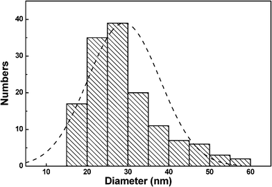 | ||
| Fig. 3 Particle size distributions of the as-prepared nanoparticles. | ||
 | ||
| Fig. 4 High resolution TEM image of the sample prepared. | ||
3.2 X-Ray photoelectron spectroscopy studies
XPS was used for the analysis of the as-prepared sample. XPS is a powerful technique for the characterization of chemical surface information,32 due to the short inelastic mean free path and sensitivity to the chemical surroundings of the photoelectrons.Fig. 5(a) shows the XPS survey of the as-prepared sample. The survey spectrum shows the copper photoelectron peaks (Cu3s, Cu2p, Cu3p and its Cu LMM Auger), the oxygen peaks (O1s and its OKLL Auger) and the photoelectron peak of the adventitious carbon (C1s). The survey spectrum shows that there were Cu, O, and C elements on the surface of the nanoparticles. No impurities on the surface of the particles were detected. The Cu and O elements result from the electrolytic Copper plate and H2O. The C element probably came from the organic surfactant molecule, which were not completely removed from the surface of nanoparticles and the adsorbed carbon dioxide.
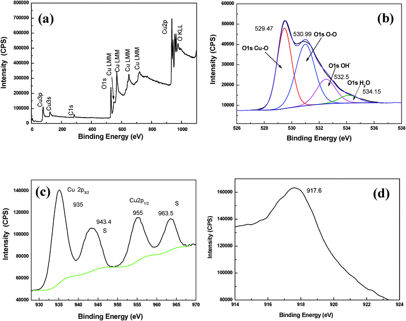 | ||
| Fig. 5 XPS spectra of as-prepared sample. (a) XPS survey spectrum; (b) O 1s; (c) Cu 2p ;(d) Cu X-ray excited auger spectra. | ||
Fig. 5 (b) shows the high resolution XPS spectra of O1s region. The O1s core-level spectrum is broad, and four O1s peaks were resolved using curve-fitting procedure. The main peaks at the lower energy of 529.47 is attributed to Cu–O, which is consistent with the literature.32 The other oxygen contributions can be counted by oxygen adsorbed on the surface of the sample the hydroxyl groups and the adsorbed H2O. Hydroxyl groups existing in the nanoparticles are attributed to the chemisorbed H2O and some H2O is also physically adsorbed on the surface of the nanoparticles.
The high resolution XPS spectra of the Cu2p are shown in Fig. 5 (c). The peaks at 935.0 and 955.0 eV are attributed to Cu2p3/2 and 2p1/2, respectively.33 Furthermore, the gap between the Cu2p3/2 and 2p1/2 is 20.0 eV, which is in agreement with the standard value of 20 eV for CuO.34 In addition to the Cu2p3/2 and 2p1/2 peaks, two shake-up satellite peaks appear at binding energies of 943.4 and 963.5 eV. The shake-up satellite peaks are evident and diagnostic of an open 3d9 shell, corresponding to Cu+ state. The peak at 935.0 eV belongs to the CuO, although it is higher than the reported energy of CuO32–35. However, it has been reported that when the component of surface CuO is small, the binding energy would shift to a higher value This may suggest that a thin layer of CuO forms on the outermost surface of the sample.35 X-ray excited auger spectra (XAES) were also recorded to distinguish oxidation states between Cu+ and Cu2+. Fig. 5(d) shows the Cu LMM spectra for the sample. It is noticed that the peak is at about 917.6, which is assigned to CuO.36 From O1s spectrum combining with Cu 2p and XAES results, we can deduce that there exists no Cu2O on the outermost surface of the sample. The fact that XRD does not show evidence of CuO phase, while XPS indicates that the surface presence of Cu2+ ions, suggests that the CuO is present only on the surface of the Cu2O nanoparticles and it forms a thin amorphous outer shell.
3.3 Formation mechanism
Formation mechanism of particles during laser ablation in liquid involves reactions in a high-temperature and high-pressure non-equilibrium process. The high-temperature (about 6000 K) and high-pressure (about 1 GPa) plasma will be produced on the solid-liquid interface quickly after one pulsed laser shot on the target.30 Subsequently, the ultrasonic adiabatic expansion of the hot plasma leads to quick cooling of the plume region and hence to formation of clusters. Finally, with the extinguishment of the plasma, the formed clusters may encounter and interact with the solvent in the surrounding solution, which leads to the particle growth and oxidation reaction. As mentioned above, during ablation and plasma formation many species including electrons, ions, free atoms, small clusters and particles expanded in the liquid. Very small particles such as atoms and clusters provide nucleation center and/or impact with the existing particles and result in grown and change in size distribution.As we known, the crystal structure of Cu2O is composed of eight cubes. In each cube, Cu atoms occupy all the fcc positions, and two oxygen atoms occupy two diagonal tetrahedral interstices. The oxidation can be qualitatively interpreted as an oxygen diffusion and lattice expansion process.37 As a result, the crystal structure and material changes from fcc Cu to cuprite Cu2O with a corresponding lattice expansion. We note that Cu and Cu2O share the high-symmetry cubic structure, while CuO is a low-symmetry monoclinic structure. There is a considerable energetic difference between the fcc structure (Cu) and monoclinic structure (CuO), as atom rearrangement and lattice/unit cell reconstruction is required, which may help to explain why crystalline CuO does not occur in nanocrystals, in addition to the possible stabilization of the oxidation state on the shell. The presence of Cu2+ ions predominately at the surface, attributed to a thin layer of amorphous CuO which may also serve as kinetic stabilization with respect to further oxidation when Cu2O nanoparticles exposed in air environment.
4. Conclusions
In summary, Cu2O nanoparticles were synthesized at room temperature by using a novel simple pulsed laser ablation route. The mean size of the Cu2O nanoparticle in diameter is about 29 nm. From structural analysis we conclude that the Cu2O nanoparticles are polycrystalline with a shell of thin layer of amorphous CuO. LAL-induced local high temperature and high pressure lead to the formation of polycrystalline Cu2O nanoparticles. We concluded that pulsed laser ablation of copper in liquid is a feasible method to synthesis of cuprous oxide nanoparticles.Acknowledgements
This work was financially supported by the National Nature Science Foundation of China (Grant No. 50831005, 51001078 and 11104150), the Key Natural Science Foundation of the Jiangsu Higher Education Institutions of China (Grant No.10KJA140043 and 08KJA510002), the Scientific Research Foundation of Taizhou University (Grant No.09ZD10), the Scientific Research Foundation of Nantong University (Grant No.09R23 and 09Z051) and the Natural Science Foundation of Zhejiang province, China (Grant No.Y4110547, and Y4110207).References
- W. Shi, K. Lim and X. Liu, J. Appl. Phys., 1997, 81, 2822 CrossRef CAS.
- I. Grozdanov, Mater. Lett., 1994, 19, 281 CrossRef CAS.
- P. C. Ohara, J. R. Heath and W. M. Gelbart, Angew. Chem., Int. Ed. Engl., 1997, 36, 1078 CrossRef CAS.
- L. F. Gou and C. J. Murphy, Nano Lett., 2003, 3, 231 CrossRef CAS.
- H. L. Xu, W. Z. Wangand and W. J. Zhu, J. Phys. Chem. B, 2006, 110, 13829 CrossRef CAS.
- M. Hara, T. Kondo, M. Komoda, S. Ikeda, K. Shinohara, A. Tanaka, J. N. Kondo and K. Domen, Chem. Commun., 1998, 357 RSC.
- P. E. Jongh, D. Vanmaekelbergh and J. J. Kelly, Chem. Commun., 1999, 1069 RSC.
- P. Poizot, S. Laruelle, S. Grugeon, L. Dupont and J. M. Tarascon, Nature, 2000, 407, 496 CrossRef CAS.
- C. M. McShane and K-S. Choi, J. Am. Chem. Soc., 2009, 131, 2561 CrossRef CAS.
- D. Snoke, Science, 1996, 273, 1351 CrossRef CAS.
- S. Ram and C. Mitra, Mater. Sci. Eng., A, 2001, 805, 304–306 Search PubMed.
- M. J. Siegfried and K. S. Choi, Adv. Mater., 2004, 19, 1743 CrossRef.
- T. D. Golden, M. G. Shumsky, Y. Zhou, R. A. Vander Werf, L. Van, A. Robert and J. A. Switzer, Chem. Mater., 1996, 8, 2499 CrossRef CAS.
- A. O. Musa, T. Akomolafe and M. J. Carter, Sol. Energy Mater. Sol. Cells, 1998, 51, 305 CrossRef CAS.
- L. L. Ermakova, V. V. Puzakov and A. D. Lanskikh, Tsvetn. Met., 1986, 7, 35 Search PubMed.
- P. McFadyen and E. Matijevic, J. Colloid Interface Sci., 1973, 44, 95 CrossRef CAS.
- A. Muramatsu and T. Sugimoto, J. Colloid Interface Sci., 1997, 189, 167 CrossRef CAS.
- Y. J. Zhu, Y. T. Qian, M. W. Zhang, Z. Y. Chen and D. F. Xu, Mater. Res. Bull., 1994, 29, 377 CrossRef CAS.
- P. R. Markworth, X. Liu, J. Y. Dai, W. Fan, T. J. Marks and R. P. H. Chang, J. Mater. Res., 2001, 16, 2408 CrossRef CAS.
- S. N. T. Kuchibhatla, S.Y. Hu, Z.Q. Yu, V. Shutthanandan, Y. L. Li, P. Nachimuthu, W. Jiang, S. Thevuthasan, C. H.Jr. Henager and S. K. Sundaram, Appl. Phys. Lett., 2009, 95, 053111 CrossRef.
- Y. Du, S. Atha, R. Hull, J. F. Groves, I. Lyubinetsky and D. R.Baer, Appl. Phys. Lett., 2004, 84, 5213 CrossRef CAS.
- S. Lee, C. W. Liang and L. W. Martin, ACS Nano, 2011, 5(5), 3736 CrossRef CAS.
- Y. Li, W. M. Paul, Y. Lei and B. S. Tom, Nanotechnology, 2007, 18, 215602 CrossRef.
- (a) H. Usui, T. Sasaki and N. Koshizaki, Chem. Lett., 2005, 34, 700 CrossRef CAS; (b) W. T. T. S. Nichols and N. Koshizaki, J. Appl. Phys., 2006, 100, 114911 CrossRef.
- (a) H. B. Zeng, P. S. Liu and W. P. Cai, Cryst. Growth Des., 2007, 7, 1092 CAS; (b) P. S. Liu, W. P. Cai and H. B. Zeng, J. Phys. Chem. C, 2008, 112, 3261 CrossRef CAS.
- (a) C. C. Huang, C. S. Yeh and C. J. Ho, J. Phys. Chem. B., 2004, 108, 4490 Search PubMed; (b) H.B. Zeng, W.P. Cai, J.L. Hu, G.T. Duan, P.S. Liu and Y. Li, Appl. Phys. Lett., 2006, 88, 171910 CrossRef.
- (a) D. Z. Tan, G. Lin, Y. Liu, Y. Teng, Y. X. Zhuang, B. Zhu, Q. Z. Zhao and J. R. Qiu, J. Nanopart. Res., 2011, 13, 1183 CrossRef CAS; (b) P. S. Liu, W.P. Liu, M. Fang, Z.G. Li, H.B. Zeng, J.L. Hu, X.D. Luo and W. P. Jing, Nanotechnology, 2009, 20, 285707 CrossRef.
- (a) S. K. Yang, W. P. Cai, G. Q. Liu, H. B. Zeng and P. S. Liu, J. Phys. Chem. C, 2009, 113, 6480 CrossRef CAS; (b) S. K. Yang, H. B. Zeng, H. P. Zhao, H. W. Zhang and W. P. Cai, J. Mater. Chem., 2011, 21, 4432 RSC; (c) S. K. Yang, W. P. Cai, H. W. Zhang, X. X. Xu and H. B. Zeng, J. Phys. Chem. C, 2009, 113, 19091 CrossRef CAS.
- H. M. Zhang, C. H. Liang, Z.F. Tian, G. Z. Wang and W. P. Cai, CrystEngComm, 2011, 13, 1063 RSC.
- (a) K. Saito, T. Sakka and Y. H. Ogata, J. Appl. Phys., 2003, 94, 5530 CrossRef CAS; (b) T. Sakka, S. Iwanaga, Y. H. Ogata, A. Matsunawa and T. J. Takemoto, Chem. Phys., 2000, 112, 8645 CAS.
- (a) G. He, Q. Fang, G. H. Li, J. P. Zhang and L. D. Zhang, Appl. Surf. Sci., 2007, 253, 8483 CrossRef CAS; (b) M. Fang, L. D. Zhang, X. L. Tan, X. Y. Hu, W. W. Yan and P. S. Liu, J. Phys. Chem. C, 2009, 113, 9676 CrossRef CAS.
- (a) Y. Li, T. Sasaki, Y. Shimizu and N. Koshizaki, Small, 2008, 4, 2286 CrossRef CAS; (b) Y. Li, T. Sasaki, Y. Shimizu and N. Koshizaki, J. Am. Chem. Soc., 2008, 130, 14755 CrossRef CAS.
- (a) J. J. Teo, Y. Chang and H. C. Zeng, Langmuir, 2006, 22, 7369 CrossRef CAS; (b) C. K. Wu, M. Yin, S. O'Brien and J. T. Koberstein, Chem. Mater., 2006, 18, 6054 CrossRef CAS.
- (a) H. H. Lin, Y. Wang and H. C. Shih, J. Appl. Phys., 2004, 95, 5889 CrossRef CAS; (b) J. Zhu, H. Chen, H. Liu, X. Yang, L. Lu and X. Wang, Mater. Sci. Eng., A, 2004, 384, 172 CrossRef.
- D. E. Diaz-Droguett, R. Espinoza and V. M. Fuenzalida, Appl. Surf. Sci., 2011, 257, 4597 CrossRef CAS.
- S. Poulston, P. M. Parlett, P. Stone and M. Bowker, Surf. Interface Anal., 1996, 24, 811 CrossRef CAS.
- M. Yin, C. K. Wu, Y. B. Lou, C. Burda, J. T. Koberstein, Y. M. Zhu and S. O'Brein, J. Am. Chem. Soc., 2005, 127, 9506 CrossRef CAS.
| This journal is © The Royal Society of Chemistry 2011 |