 Open Access Article
DOI:
10.1039/C1NR10806A
(Paper)
Nanoscale, 2011,
3, 4830-4839
Assorted analytical and spectroscopic techniques for the optimization of the defect-related properties in size-controlled ZnO nanowires†
Received
13th July 2011
, Accepted 10th September 2011
First published on 10th October 2011
Abstract
In this article, the important role of the intrinsic defects in size-controlled ZnO nanowires (NWs) which play a critical role in the properties of the NWs, was studied with a combined innovative experimental analysis. The NWs prepared by both the aqueous solution method and chemical vapour deposition process were of increasing length and decreasing size-to-volume (S/V) ratio. The combined approach involved different analytical and spectroscopic techniques and from the correlation between the different measurements, the concentration of the oxygen vacancies jointly with the zinc interstitials defects and the zinc vacancy defects was observed to be positively or negatively correlated, respectively, with the magnitude of the photoluminescence intensity and radiative lifetimes. Furthermore, the experimental results also suggest that the oxygen vacancy defects are not only spatially located on the surface of the NW but an increasing fraction of the total oxygen vacancy defects connected with the green emission is also located in an annulus region beneath the surface as the ZnO NWs elongate. On the other hand, as the donor concentration plays a critical function in the properties of the ZnO NWs, an analytical model was derived for the calculation of the donor concentration of the NWs directly from its reverse-biased current–voltage characteristics obtained from the conductive atomic force microscopy measurements.
1. Introduction
Functional one-dimensional (1D) nanostructures of semiconductor and metallic oxides are very important for the next generation of electrical, nano-1,2 and optoelectronics devices. In this aspect, zinc oxide (ZnO) is a compound semiconductor with a hexagonal wurtzite structure and possesses a number of fundamental advantages which include a direct wide band gap of 3.37 eV where its low power threshold enables optical pumping at room temperature.3 In addition, the exciton binding energy (60 meV) in ZnO being larger than the room temperature thermal energy also permits stable exciton emission at room temperature4 and ZnO is also used in alloy systems such as ZnCdO and ZnMgO for bandgap engineering.5 Hence, the continual investigation of 1D ZnO nanostructures, particularly on ZnO nanowires (NWs), over the years has established ZnO as an essential candidate for a multifunctional material for the commercialization of optical and electronic devices such as photodetectors, ultraviolet light emitting diodes, gas sensors and field effect transistors.6–9 The performance and properties of the ZnO 1D based devices are intimately related to the native intrinsic defects or artificially incorporated defects where the defects alter the structural, optical, electrical and magnetic properties of the semiconductor. Various studies have been focused on the formation and controlled artificial incorporation/introduction of intrinsic defects as well as the evolution of point defects in ZnO. Such techniques include annealing in different atmospheres or temperatures,10 self-ion implantation and energetic electron irradiation,11 and doping of impurities12 as a way of engineering the material properties of the defect-induced ZnO in accordance to a particular technological requirement. However, native intrinsic defects are always inadvertently present in the synthesized ZnO NWs and hence an understanding of these defects is essential for optimizing the properties and performance of the 1D ZnO NWs. For example, it is widely acknowledged that nominally undoped ZnO exhibits n-type behavior without the influence of any intentional doping,13 where it has been observed to be closely related to the presence of native intrinsic defects such as oxygen vacancies and zinc interstitials.14 Importantly, few articles have reported on the influence of the length and corresponding surface-to-volume (S/V) ratio of the ZnO NW on the concentration and variation of the different types of native intrinsic defects in the NW as well as the correlation between them.
In this article, we use a combined experimental approach for a systematic analysis to understand the important role of the native intrinsic defects in influencing the properties of the ZnO NWs. We are able to provide such an understanding due to the use of both the aqueous solution method and a modified chemical vapour deposition (CVD) process to synthesize ZnO NWs of different lengths and sizes where the variation of the concentrations of intrinsic native defects can be easily distinguished between the different samples. X-Ray photoelectron spectroscopy (XPS) and energy dispersive X-ray spectroscopy (EDS) measurements were utilized to study the chemical state and composition of the ZnO NWs in order to understand the important function of certain native defects such as oxygen vacancies (Vo) and zinc interstitials (Zni) in the n-type conductivity and optical properties of the ZnO NWs. Conversely, optical characterizations of the NWs were performed with confocal photoluminescence (CPL) and confocal time-resolved photoluminescence spectroscopy (CTRPLS) which is a contactless method for understanding the dynamics of the carriers involved in optical processes such as the temporal information on the recombination lifetime as well as the optical emissions at specific wavelengths from the intrinsic defects in the ZnO NWs.15 Importantly, with the use of different spectroscopic techniques, the connection between the PL intensities and radiative lifetimes with the concentration of native intrinsic defects and their spatial location on and beneath the surface of the NWs with different S/V ratios and lengths was investigated. The increase/decrease of the various parameters was understood in terms of some physical mechanism due to the incorporation of the intrinsic defects related to the decrease in the S/V ratio of the synthesized NWs. On the other hand, conductive atomic force microscopy (CAFM) is a viable method for obtaining the current–voltage (I–V) characteristics of the ZnO NW arrays without the prior metallization requirement of the ZnO NW arrays as the probe tip could effectively function as the electrode for the I–V measurements. Hence by considering the conduction mechanism of the reverse biased I–V characteristics in the NWs, an analytical equation (with the use of Páde approximations) is derived for obtaining the donor concentration of the ZnO NW arrays with different lengths directly from its corresponding I–V characteristics. The validity of the analytical model was verified by Hall measurements and similarly the donor concentration was positively correlated with the increase in the concentration of Vo and Zni. Such an understanding could possibly provide a deeper understanding of the relationships between the native defects and donor concentrations in the ZnO NW when its size and length varies as an approach for tuning its electrical and optical properties for reliable device applications.
2. Experimental details
2.1. Synthesis of the ZnO NW arrays
All chemicals (analytically pure) were purchased from Sinopharm Chemical Reagent Co., Ltd. and used without further purification. A (100) silicon (Si) wafer was used as a substrate, which was cleaned with ethanol and acetone in an ultrasonic bath for half an hour, followed by etching in a mixed solution of 20 mL of ammonia hydroxide (25%), 20 mL of H2O2 (30%) and 100 mL of deionized water. To minimize the substrate effect on the subsequent electrical measurements on the ZnO NW arrays, the ZnO NWs were fabricated on n-type Si substrate with very low resistivity value of 0.006 to 0.008 Ω cm. An alcoholic solution of zinc acetate (0.02 M) was spin-coated 5 to 7 times on the cleaned Si substrate, followed by annealing in air at 300 °C for 30 minutes. ZnO seed layers are thus formed on the substrate for the subsequent growth of the ZnO nanowire arrays. 1.859 g of zinc nitrate hexahydrate (Zn(NO3)2·6H2O, 98%) and 0.876 g of hexamethylenetetramine (HMTA, C6H12N4, 98%) were dissolved into 250 mL of deionized water. Subsequently, the Si substrate with the ZnO seed layers was immersed (with the seed layers facing down) in the aqueous solution at 85 °C for 3 h. Finally, the substrate was removed from the aqueous solution, rinsed with distilled water for several times, and dried at room temperature.
On the other hand, the longer ZnO nanowire arrays were synthesized via a classical CVD process in a single-zone horizontal tube furnace. All chemical reagents were analytical grade and used without further purification. The Si (100) substrate was first washed with absolute alcohol (99.7%) and then with acetone (99.5%) in an ultrasonic bath. Then it was etched in a mixed solution of 20 mL of ammonia hydroxide (25%), 20 mL of H2O2 (30%), and 100 mL of deionized water at 80 °C. An alcoholic solution of zinc acetate dehydrate (2 M) was spin-coated 5 to 7 times on the substrate followed by annealing in an oven at 120 °C for half an hour. This simple spin-coating method was used to obtain a film of ZnO crystal seeds instead of the relatively costly sputter-coating. The source material for the CVD was pure ZnO powder (0.5 g, 99.0%) mixed with graphite (0.5 g, 99.85%). After grinding, the mixtures were spread in an alumina boat which was placed at the center of the furnace tube. The substrate covered with a film of ZnO seeds was placed above the source material and the distance between them was about 2–5 mm. Subsequently, 70 sccm (standard cubic centimetres per minute) of argon gas and 2 sccm of oxygen gas was introduced into the reactor and the pressure in the tube was adjusted to 200 mbar. The temperature was heated up to 950 °C at a rate of 25 °C min−1 and this temperature was held constant for 5 to 20 min. After reaction, the furnace was cooled naturally to room temperature. Please refer to the ESI† for the details about the type of equipment used for the morphological, chemical, optical and electrical characterization of the synthesized ZnO NW arrays. In particular, the description of the experimental setup to obtain the carrier concentration of the ZnO NW arrays using the Van der Pauw four probe technique16 with a square configuration is provided.
3. Results and discussions
3.1. Structure and morphology
The SEM images showing the side view of the as-synthesized ZnO NWs with different lengths are shown in Fig. 1(a)–(d) where the length of the vertical ZnO NW arrays is about 2 μm [Fig. 1(a)] and 150 μm [Fig. 1(d)] as prepared by the solution method and after a growth time of 20 minutes by the CVD process, respectively. Fig. 1(e) and (f) show the typical 45° tilted view SEM image showing the morphology of the as-prepared vertical ZnO NW arrays by the aqueous solution method and the CVD process, respectively. It was observed that the ZnO NWs grown by the two methods are dense and the height of the NWs in the array is rather uniformly long. In addition, the NWs also are uniformly distributed on the surface of the Si substrate where most of the NWs are vertically quasi-aligned with an inclination towards the Si surface.
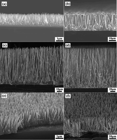 |
| | Fig. 1 Side view of the ZnO NW arrays showing the length of the synthesized NWs where they were prepared by the (a) aqueous solution method and by the CVD process where the temperature at 950 °C was maintained for (b) 5 min, (c) 11 min and (d) 20 min, respectively. The typical 45° tilted view SEM image showing the distribution of the NW arrays prepared by the (e) aqueous solution method and by the (f) CVD process. | |
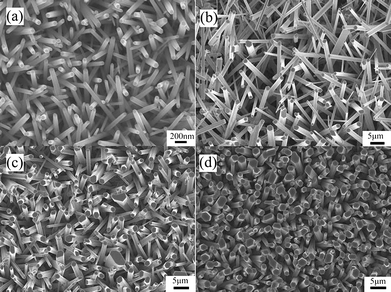
For a better examination of the surface morphology of the ZnO NWs, the close-up, higher magnification top view SEM image of the vertical ZnO NW arrays in the 4 samples are displayed in Fig. 2(a)–(d). From the images, it can be deduced that the shape of the nanowires is hexagonal and the diameter of the solution prepared NWs is distributed in the range of 50 nm to 150 nm with an average value of 100 nm while the diameter of the CVD prepared NWs is larger in the range of hundreds of nm or in the micrometre range. In addition, it was also determined statistically from Fig. 2 that the average diameters of the ZnO NWs increase from those in Fig. 2(a)–(d) where fewer ZnO NWs with smaller diameters in the nm range were observed (Fig. 2(d)). The four samples with different average NW diameter of 100 nm, 500 nm, 1 μm and 1.5 μm are named as sample A, B, C and D, respectively.
 |
| | Fig. 2 Typical top view SEM image of the vertical ZnO NW arrays showing the cross-section of the as-synthesized NWs in sample (a) A, (b) B, (c) C and (d) D. | |
Fig. 2 shows that the growth time during the CVD process can affect the diameter of the ZnO NWs. While not implying that the growth time in our CVD process will have a drastic effect on the diameter of the ZnO NWs, but during the synthesis process, the ZnO NWs can grow in both the vertical (c-axis direction) and radial direction with extended growth time.17 Hence, this may lead to more NWs in sample D having a slightly larger diameter with a small resultant increase in the average diameter of the NW arrays. However, it must be stressed that the length of the NW increased at a much faster rate as compared to the small increase of the diameter by comparing Fig. 1 and 2. On the other hand, the TEM images of the ZnO NWs were also obtained as the SEM images may not provide the necessary resolution for a closer examination of the surface roughness of the NWs. Fig. 3 shows the TEM images of some of the synthesized NWs where the diameter of a single NW from sample B [Fig. 3(a)] is about 350 nm which is in good agreement with the SEM image in Fig. 2(b). The images show a rough surface morphology which suggests the presence of a high density of surface states.
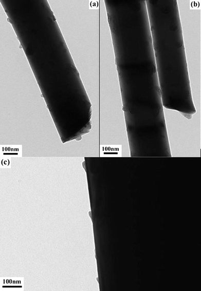 |
| | Fig. 3
TEM images of the ZnO nanowires in sample (a) B, (b) A and (c) D. | |
By approximating the ZnO NW as a cylinder and from a purely geometric viewpoint the surface to volume ratios of the NWs are given by
| | 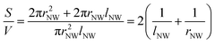 | (1) |
where
lNW and
rNW is the average length and radius of the NW, respectively.
From eqn (1) and from Fig. 1 and 2, it was seen that the S/V ratio of the synthesized NWs in this article decreases from sample A to D. [The S/V ratio of the NWs taking into consideration the surface recombination layer of a finite thickness is given in ref. 18.]
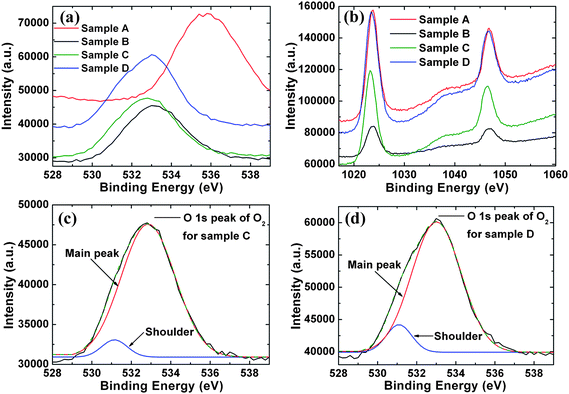
XPS analysis was utilized to understand the surface chemical state of the synthesized ZnO NWs and Fig. 4(a) displays the XPS O 1s spectrum of the ZnO NW arrays in samples A to D. The shape of the XPS patterns was similar for the 4 samples and hence Fig. 4(b) show the Zn 2p spectra for samples A to D which indicate that the ZnO NW surface consists of the same elements where the peaks observed at about 1022 eV and 1045 eV (related to the Zn–O bonding) correspond to Zn 2p3/2 and Zn 2p1/2, respectively.19 On the other hand, the asymmetry observed in the O 1s peak for the samples indicates that the O 1s peak should have more than one origin, where Fig. 4(c) and (d) show in more detail the XPS high resolution spectra of the O 1s peak for samples C and D, respectively. The O 1s peak for samples B to D can be consistently deconvoluted into a main Gaussian curve centered at 533.0 eV and a shoulder peak centered at 531.2 eV. The lower binding energy component at around 531.2 eV has been attributed to oxygen deficiencies or vacancies within the ZnO matrix20 whereas the higher binding energy component is probably due to some surface hydroxide species on the NWs.21 Comparing Fig. 4(c) and (d), it was observed that the intensity of the O 1s component at 531.2 eV is lower for sample C as compared to sample D and the intensity of this component is related to the concentration of Vo.20 On the other hand, Fig. 4(a) shows the shift of the O 1s peak to higher energy for sample A which implies the increase of oxygen atoms on the surface of the NWs (reduction in the concentrations of Vo) prepared by the aqueous solution method.22 This indicates that the ZnO NWs prepared by the CVD process (samples B to D) contain more oxygen-deficient states as compared to sample A. Hence the analysis of the O 1s peak suggests that the surfaces of the longest ZnO NWs in sample D possess the highest concentration of oxygen vacancies.
 |
| | Fig. 4 (a) XPS spectra of the oxygen 1s peak and (b) XPS spectra of the Zn 2p peak corresponding to the ZnO NWs in the four samples A to D. The fitting of the oxygen 1s peak by Gaussian functions corresponding to (c) sample C and (d) sample D, respectively. | |
For a more quantitative analysis of the surface stoichiometry of the ZnO NWs to confirm the above observation, the relative ratio of Zn/O can be obtained using the XPS peak area of Zn and O and their elemental sensitivity factor given by,23
| |  | (2) |
where
n(Zn)and
n(O) are the atomic numbers of the Zn and O elements,
A(Zn) and
A(O) are the areas under the Zn 2p and O 1s peaks and
S(Zn) and
S(O) are the elemental sensitivity factors of Zn and O at 4.8 and 0.66, respectively.
23
On the other hand, since the XPS spectroscopy can only probe up to about 10 nm beneath the surface of the NWs,24 while the X-ray in the energy-dispersive X-ray spectroscopy (EDS) measurements can penetrate to a deeper depth of about 1 to 2 μm,25 the bulk stoichiometry of the ZnO NWs could be obtained from the EDS measurements. Quantitative analysis of the results shows that the surface and bulk atomic ratios of Zn to O (Zn/O) corresponding to the 4 sets of samples (tabulated in Table 1) are all greater than unity and are likewise positively correlated with the increase in the length (and corresponding decrease of the S/V ratio) of the synthesized ZnO NWs. Hence the XPS and EDS analysis implies that there are oxygen deficiencies in the ZnO NWs and the native intrinsic defects vary distinctly with the length of the NWs. (A similar level of oxygen deficiencies at about 20%26 or at even higher level had also been previously observed in ZnO nanostructures.25) Conversely, as there is an easier formation of Zni due to dissociation under high temperature conditions,27 the extended growth time for the longer NWs during the CVD process may have led to a surplus concentration of Zni incorporated in the NWs. The excess zinc atoms in the ZnO crystal lattice become ionized and preferably diffuse and accumulate at interstitial positions in the ZnO crystal lattice which results in an increase of interstitial Zn atoms and Zni defects as well as a decrease in the concentration of zinc vacancies, VZn (the concentration of VZn should be reduced in Zn rich conditions).28 Therefore the concentration of the Vo jointly with Zni defects as well as the VZn defects increases and decreases, respectively, on the surface and in the bulk for the longer synthesized ZnO NWs. (Please refer to the ESI† for the EDS spectrum corresponding to the four samples.)
Table 1 Length, S/V ratio as calculated from eqn (1) and the weight and atomic percentages of the zinc and oxygen element from the analysis by EDS of the samples. The surface and bulk atomic ratio of Zn to O from the XPS and EDS measurements, respectively, are also included in the table
| Sample |
Length/μm |
S/V ratio/μm−1 |
Element Zn wt% |
Element O wt% |
Element Zn atomic% |
Element O atomic% |
Surface Zn/O ratio from XPS |
Bulk Zn/O ratio from EDS |
| A |
2 |
21.00 |
81.41 |
18.59 |
51.73 |
48.27 |
1.06 |
1.07 |
| B |
20 |
4.10 |
82.37 |
17.63 |
53.35 |
46.65 |
1.12 |
1.14 |
| C |
68 |
2.03 |
83.09 |
16.91 |
54.61 |
45.39 |
1.19 |
1.20 |
| D |
150 |
1.35 |
83.35 |
16.65 |
55.05 |
44.95 |
1.24 |
1.22 |
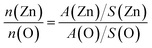
Fig. 5(a) shows the spatially resolved PL intensity mapping of sample D by scanning an area of 38 μm × 35 μm using the confocal microscope. The figure shows that the emission intensity is inhomogeneously distributed. The regions of clear and stronger emission in Fig. 5(a) that correspond to the ZnO NWs typically display a hexagonal shape with diameter in the range of between 1 and 2 μm, which corresponds to the hexagonal shape similarly observed in the top view SEM image in Fig. 5(b) corresponding to sample D. The weaker emitting NWs are probably shorter and thus not in the focal plane. The surface morphology of the ZnO NWs was also investigated with AFM using a 50 nm platinum (Pt)-coated Si probe tip. Fig. 5(c) shows the typical AFM topography of sample D in a scan area of 2 μm × 2 μm at a slow scan rate of 0.1 Hz which also similarly shows that the ZnO NWs are hexagonally shaped with a diameter of about 1 μm which is in agreement with the SEM image in Fig. 5(b).
 |
| | Fig. 5 (a) Spatially resolved PL intensity microscopic image, (b) top view SEM image and (c) AFM image corresponding to the arrays of ZnO NWs in sample D. | |
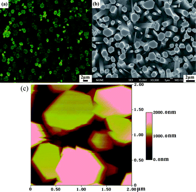
The room temperature CPL spectra of the NWs around the excitation spot for the 4 samples consist of a dominant green band centered at around 510 nm and an extremely weak and broad UV emission at 380 nm where the yellow-orange (590–640 nm) PL band usually ascribed to excess oxygen (oxygen interstitials)29,30 was not observed in the CPL spectrum as shown in Fig. 6(a). The UV emission arises due to the band to band transition from the direct electron–hole pair recombination between the conduction and valence band.30 In addition, the dominant visible PL band also suggests that there is a high concentration of surface defects and this is corroborated by the rough surface morphology observed in the TEM image, as shown in Fig. 3. The lowest excitation wavelength, λex that could be used for the CPL measurements is 375 nm. By utilizing a xenon (Xe) lamp where the wavelength of excitation could be varied, ensembles of NWs in samples A to D could be excited at a lower wavelength (λex = 270 nm) for additional PL measurements. Fig. 6(b) shows that two new PL bands centered at around 400 nm and 420 nm could be observed in the PL spectrum for samples A to D where the UV band at 380 nm is still very weak. Conversely, the luminescence peak at 400 nm has been suggested to be due to the recombination of free excitons through an exciton–exciton collision process31 while the peak at 420 nm has been attributed to the interstitial Zn ions32,33 in the ZnO lattice. For instance, the increase of the PL intensity at 420 nm [in Fig. 6(b)] can be correlated to a higher concentration of Zni defects with the increase of the NW length from sample A to D, and this is in agreement with the results from the XPS and EDS measurements. Please refer to the ESI† for some further details on the comparison between the PL and CPL spectra and XRD analysis of the crystalline quality of the ZnO NW arrays. From the XRD analysis, the red-shift of the green CPL and PL emission spectra band between the different samples could be due to some bandgap narrowing effects as a result of the intrinsic stress in the NW from the incorporation of the native intrinsic defects in the NWs or could be due to the spatial variation of the Vo defects in the NW.
 |
| | Fig. 6 (a) CPL spectra obtained with a pulsed diode laser (λex = 375 nm) and (b) PL spectra obtained with a Xe lamp (λex = 270 nm) corresponding to the four samples A to D. | |
From the above EDS, XPS, CPL and PL measurements, it is observed that sample A (synthesized by the hydrothermal method) contains a lower concentration of defects (e.g. Vo and Zni) as compared to samples B to D (synthesized by the hydrothermal method). Although ZnO NWs synthesized by the hydrothermal method usually contain a higher concentration of defects as compared to the CVD method, our experimental results are also in agreement with some reports that ZnO NW synthesized by the hydrothermal method is of good quality and contains a low concentration of defects.34–36 While it is beyond the scope of this article to explain the factors and mechanisms resulting in the variation of the defect concentration in the ZnO NWs synthesized by the hydrothermal method, nonetheless from Fig. 1 and 2, it is also observed that the size and corresponding S/V ratio increases and decreases, respectively, from sample A to D. Importantly, this is well correlated with the corresponding increase of the concentration of defects from sample A to D and hence we propose that a comparison of the subsequent results can also be made concurrently between the different samples according to the difference in their size or morphology.
3.3.1. Variation of the concentration of Vo defects in the ZnO NW of different sizes and lengths.
Although the nature of the defect responsible for the green emission is still not fully clear and many hypotheses have been proposed to explain the emission originating from intrinsic defects or impurities,37 this emission, however, is typically and widely accepted to be associated with oxygen vacancies.30,38–40 However, there is still some uncertainty on the exact recombination model of the green emission involving the oxygen vacancies (please see the ESI† for more details). In addition, density functional calculations have also shown that Vo is a deep donor and is also the dominant intrinsic defect under both Zn-rich and O-rich conditions.41 From Fig. 6(a) and (b), a good correlation is observed between the increase of the intensity of the observed green PL and CPL band with the increase of the NWs length (samples A to D) and consequently with the increase of the Vo defect concentration from the XPS and EDS measurements. Such a trend has also been observed earlier by other researchers in the field.40 On the other hand, the penetration depth of the excitation light (at 270 and 375 nm) used in the PL and CPL measurements is in the range of tens to hundreds of nm. For instance, the penetration depth of the excitation light at 325 nm for ZnO is about 60 to 120 nm.42 Therefore we believe that the defects responsible for the green luminescence in the ZnO NW samples might originate from the oxygen vacancies that are located not only on the NW surface but also in an annulus region in the NW beneath the ZnO NW surface. In support of this hypothesis, the decrease of the S/V ratio for the longer NWs indicates that there exist lesser surface states39 per volume for the longer NWs. However, the increase of the green PL and CPL intensity correlates directly with the increase of the concentration of Vo [Fig. 6(a) and (b)] as the NWs elongate, which is in agreement with the XPS measurements. To reconcile these two observations, besides the Vo defects existing on the surface of the NW, it is also necessary that a larger portion of the total concentrations of the oxygen vacancies are located in an annulus region which is beneath the ZnO NW surface as the length of the NWs increases. This is substantiated by the quantitative analysis of the EDS measurements where the increasing bulk atomic Zn/O ratio in Table 1 implies that the concentration of the Vo defects beneath the surface of the NWs similarly increases as the NWs elongate.
Furthermore, this viewpoint is supported by the PL measurements in Fig. 6(b) where a shorter excitation wavelength (higher photon energy) is used for the measurements, which correspond to a slightly deeper penetration depth in the samples. It was observed that at spatial locations deeper beneath the surface of the NWs, the increase of the green PL intensity (between 488 nm and 507 nm) is similarly correlated with the increase of the length of the NWs (and corresponding decrease of the S/V ratio). This signifies that Vo defects exist at a spatial location deeper in the NW and a higher concentration of Vo exists in the interior of the longer NWs as compared to the shorter NWs. Hence from the results, we infer that a larger fraction of the oxygen vacancies should exist in an annulus region beneath the surface of the synthesized NW as its length and S/V ratio increases and decreases, respectively. The diagram in Fig. 7 serves as an illustration of the details pertaining to this discussion. On the other hand, the visible emission bands also could not have originated from impurities as no impurity was detected in our ZnO NW sample with the EDS measurements. In addition, it was also observed that the concentration of the Vo defects responsible for the green emission on the surface as well as in the annulus region of the as-synthesized NWs was not influenced by the range of applied light intensity used in the experiments (please refer to the ESI† for further details).
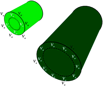 |
| | Fig. 7 Illustrative diagram which shows the different distribution of Vo defects on the surface and in the annulus region beneath the surface of the NW for ZnO NWs of different lengths and S/V ratios. | |
3.4. Luminescence lifetimes
In order to obtain more insight into the luminescence behaviour of the ZnO NWs, the CTRPLS measurements was performed on the ZnO NWs. Fig. 8 shows the temporal decay curves of PL intensity where a rapid decrease of the PL intensity for samples A to D was observed during the first few ns. The experimental decay curves of the ZnO NWs samples can be fitted with a biexponential function, with a fast and slow time constant with a relationship given by| |  | (3) |
where τ1 and τ2 are the time constants of the fast and slow radiative decay, respectively. Similarly, A1 and A2 are the constants which determine the contributions of the fast and slow decay components, respectively.
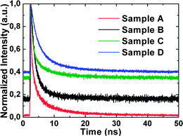 |
| | Fig. 8 Room temperature normalized TRPL spectra for samples A to D. | |
The lifetime parameters upon excitation at 375 nm, obtained by fitting the experimental curves of samples A to D to the biexponential function, are summarized in Table 2. On the other hand, the measured PL decay will be strongly dependent on the interplay and relative value of τ1 and τ2 as well as their relative contributions (calculated as (A1)/(A1 + A2) and (A2)/(A1 + A2)) to the PL intensities. These values are shown in Table 2 where the weighted average relative contribution of τ1 and τ2 is about 67% and 33%, respectively. Both components refer to a radiative decay process which implies that there are two different emissive centers or luminescent states. The two different radiative decay pathways for the synthesized ZnO NWs could be due to the oxygen vacancies located at the surface or at spatial locations deeper in the NW (e.g. Vo in the annulus region in Fig. 7). According to a recombination model proposed for the green PL emission, the rate of the tunneling recombination between a surface-trapped hole with an electron in an oxygen vacancy defect decreases for deeper spatial locations beneath the surface.39 Hence, the fast radiative decay could be due to the oxygen vacancies on the surface of the NW. Conversely, the slow radiative decay may be due to the Vo defects located in spatial locations deeper in the NW due to the decrease of the recombination probability for the Vo defects away from the surface, which will lengthen the lifetime of the radiative decay process.
Table 2 Length, S/V ratio as calculated from eqn (1) and the surface and bulk Zn/O composition ratio of the ZnO nanowires. The fast (τ1) and slow (τ2) time constant from the fit to the biexponential function in eqn (3), the average lifetime (τaverage) as well as the relative contributions of the fast decay component (WA1) and slow decay component (WA2) to the luminescent from the nanowires are also included in the table
| Sample |
Length/μm |
S/V ratio/μm−1 |
Surface Zn/O ratio from XPS |
Bulk Zn/O ratio from EDS |
τ
1/ns |
WA1 (%) |
τ
2/ns |
WA2 (%) |
τ
average/ns |
| A |
2 |
21.00 |
1.06 |
1.07 |
0.93 |
70.23 |
6.15 |
29.77 |
2.07 |
| B |
20 |
4.10 |
1.12 |
1.14 |
1.16 |
64.43 |
6.23 |
35.57 |
2.48 |
| C |
68 |
2.03 |
1.19 |
1.20 |
1.01 |
63.77 |
6.88 |
36.23 |
3.14 |
| D |
150 |
1.35 |
1.24 |
1.22 |
2.23 |
69.64 |
9.58 |
30.36 |
4.46 |
On the other hand, it is also observed in Table 2 that both components of the luminescence lifetime decay are smaller for the shorter ZnO NWs (i.e. sample A) as compared to the longer NWs. The shorter radiative lifetime associated with the shorter ZnO NWs implies that the non-radiative processes become more predominant where the photo-generated carriers will have a higher probability of following a non-radiative decay pathway instead of radiative recombination. The non-radiative processes are solely governed by certain point defects incorporated with VZn, forming the VZn − X complexes43 where they function as dominant non-radiative recombination centers (NRCs),43 as the influence by the single point defects is minimized because according to A. F. Kohan et al., a single point defect may not serve as an NRC.44 This is in agreement with the stoichiometry imbalance in our samples as the surface and bulk Zn/O composition ratio (reproduced in Table 2) can be used as a measure of the concentration of VZn defects. A good correlation is observed between the increasing radiative lifetime (fast and slow component) and the increasing surface and bulk Zn/O composition ratio which implies that the concentration of VZn defects (see Section 3.2) and hence the density of the VZn – X-related defect complexes (NRCs) decreases from sample A to D. Similarly, this will also lead to a decrease of the non-radiative recombination processes (hence an increase of the radiative lifetime) from sample A to D. This shows that the non-radiative decay process may be related to the carrier trapping at VZn and their complexes in the ZnO bandgap. On the other hand, it was also observed that as the length of the synthesized ZnO NWs increases, the corresponding decreasing S/V ratio could lead to a decrease (slowing) of the scattering rate of the excitons with the surface of the ZnO NWs, which may increase the radiative lifetime due to some surface recombination process.45 (Please refer to the ESI† for more details, e.g. slope of the decay rate of the samples.)
3.5.
CAFM measurements and the derivation of the analytical model
The I–V measurements of the ZnO NW arrays were performed by selecting an appropriate NW from the surface topography image first acquired in the AFM mode. Subsequently, the I–V curves were obtained by applying an external voltage bias (from +5 V to −5 V) between the 50 nm Pt-coated Si probe tip placed on top of the ZnO NW and the sample stage (where the Si substrate rests upon). The schematic diagram in Fig. 9(a) illustrates the measurement setup. A Schottky barrier is formed between the Pt-coated probe tip and the ZnO NW at the contact interface46 where the current will flow vertically through the probe tip–ZnO NW Schottky interface. Silver paste was applied on the edge and underside of the sample to ensure better electrical connectivity of the bottom of the ZnO nanowire arrays on the Si substrate surface with the measurement circuit as well as to ensure that the sample is well grounded. The typical I–V curves corresponding to the ZnO NWs of different lengths measured at room temperature are shown in Fig. 9(b) where the current in both the forward and reverse bias region for the longer ZnO NW is smaller as compared to the shorter ZnO NW. This could be due to the increased resistance for charge transport as the increased resistivity of the longer NWs is due to higher donor concentration (from the Hall measurements).
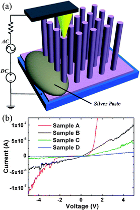 |
| | Fig. 9 (a) Schematic diagram showing the use of an AFM probe to measure the I–V characteristics corresponding to an individual ZnO NW in a vertical NW array. (b) I–V characteristics from a vertical ZnO NW corresponding to samples A to D with a conductive AFM probe. | |
On the other hand, the I–V characteristics in Fig. 9(b) also display a rectifying behaviour in the negative voltage region with a low rectification ratio IF/IR (ratio of forward to reverse current measured at V = ±4 V) between 3 and 10 for the four different nanowires. As the rectification ratio depends on the interface between the probe tip and the ZnO NW, this observation could be correlated to the prevalence and non-negligible effects of interface states between the probe tip and ZnO which originate from surface imperfections such as defects on the ZnO NW surface (evident from the TEM images in Fig. 3).47 From the determination of the saturation current, Is,Pt–NW, by extrapolating the logarithmic plot of the I–V characteristics in Fig. 9(b) under forward bias to V = 0 V, the barrier height of the Schottky potential barrier at the probe tip–ZnO NW interface, ϕPt–NW for sample A to D can be determined and is given by48
| | 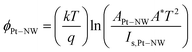 | (4) |
where
APt–NW = π
r2NW,average is the effective contact area at the probe tip–ZnO NW interface which is assumed (for simplicity) to be equal to the average cross-sectional area of the NWs and
rNW,average is the average radius of ZnO NW as estimated from the SEM images in
Fig. 2 corresponding to a particular sample.
q is the elementary charge,
k is the Boltzmann's constant, and
T is the absolute temperature in Kelvin.
A* = 4π
qm*ek2/
h3 is the effective Richardson constant (without considering the effects of quantum mechanical reflection and optical phonon scattering) with a theoretical value of 32
AK−2 cm
−2 for
m*e = 0.27
mo48 where
h,
m*e and
mo are the Planck's constant, electron effective mass and rest mass respectively.
The donor concentration of the ZnO NW indirectly affects many of its electrical properties, hence a simple way of obtaining the donor concentration directly from the I–V characteristics will be very useful for characterization purposes. Under reverse bias and in low-dimensional nanostructures, the Schottky potential barrier at the probe tip–ZnO NW interface, ϕPt–NW becomes narrower and the tunnelling current of electrons from the probe tip to ZnO through the reverse biased Schottky barrier become more significant. At room temperature and for reverse bias voltage, the tunnelling current is predominantly due to the thermionic field emission current48 and the current density through ϕPt–NW is given by48
| | 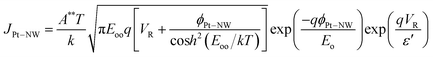 | (5) |
where
| | 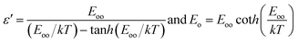 | (6) |
and
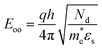
is the characteristic energy relating to the tunnelling probability.
In eqn (5), A** is the reduced effective Richardson constant which takes into account of the effects of optical-phonon scattering and quantum mechanical reflection.48εs = εrεo is the permittivity of the ZnO NW, εr = 8.3649 is the relative permittivity of the ZnO NW used in this study (corresponding to thin ZnO film as the quantum confinement effect in our ZnO NW is not significant because rNW is larger than the ZnO exciton Bohr radius50) and εo is the permittivity of free space. Nd is the donor concentration in the ZnO NW expressed in m−3. It should be clarified that in eqn (5), ϕPt–NW is in volts. For a detailed description of the algebraic derivation of the analytical model, please refer to the ESI† for the full details as only a very brief outline of the steps is described below. Firstly, eqn (6) is substituted into the exp(qVR/ε′) term of eqn (5) and the result is simplified followed by taking the natural logarithms on both sides of the resultant equation. After a series of algebraic manipulations, it was realized that in order to obtain a mathematical expression which permits further algebraic evaluation, the Padé approximant technique51 would have to be used to express one of the algebraic terms by an approximate rational expression. Subsequently, a long and complicated expression was obtained where the terms with the variable “VR” and “ln VR” can be grouped together. Therefore the donor concentration can be obtained directly from the slope of the reverse bias ln IR − VR characteristics corresponding to the ZnO NW (denoted as GR) given by
| | 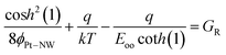 | (7) |
and by rearranging the above equation and using the definition of
Eoo, the donor concentration of a single ZnO NW is given by
| | 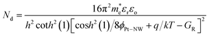 | (8) |
It should be noted that the unit of Nd in eqn (8) is in m−3 and multiplying by a factor of 1 × 10⁻⁶ is needed to convert the doping concentration to cm−3 (m−3 = 1 × 10⁻⁶ cm−3). From the reverse IR − VR characteristics in Fig. 9(b), an almost linear variation of the reverse current is observed for the semi-log reverse bias ln IR − VR characteristics corresponding to the four sets of ZnO NW arrays. From the slope of the plots and eqn (8), the donor concentration of the ZnO NW from samples A to D is shown in Fig. 10. The donor concentration calculated from the analytical model is in good agreement with the carrier concentration obtained from the Hall measurements for samples A and D which verifies the validity of the assumptions used in the analytical model. On the other hand, the concentration of Vo and Zni defects (from the stoichiometric analysis) is also positively correlated with the increase in the length and donor concentration of the synthesized ZnO NWs. This could be possibly due to the attractive force between the Vo and Zni defects present in the NWs,14 which function as a source of donors for the n-type conductivity in the NWs as envisaged from first principle theoretical calculations.52 (Please refer to the ESI† for more details.)
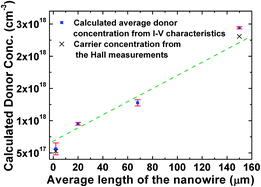 |
| | Fig. 10 Comparison of the calculated donor concentration as a function of the average NW length with the carrier concentration obtained from the Hall measurements. The error bars indicate the standard deviations of the donor concentration calculated from the I–V characteristics corresponding to the ZnO NW using eqn (8). | |
4. Conclusions
ZnO NWs of different lengths from 2 μm to 150 μm and sizes were prepared by both the aqueous solution method and the CVD process. Various analytical and spectroscopic techniques for the structural, chemical, optical and electrical characterization of the NWs were performed. The SEM images show that the average diameter and length of the NWs increases when the growth time of the NWs was extended, thus resulting in a decreasing S/V ratio for the longer NWs. In addition, the XPS, EDS, CPL and PL measurements exhibit a clear correlation of the increase of the oxygen vacancies, zinc interstitials, PL intensity and decrease of the zinc vacancies, respectively, with the increase of the length of the ZnO NWs. Consolidation of the experimental observations from the different analytical and spectroscopic techniques suggests that Vo may be the origin of the green emission from the ZnO NWs. Additionally, it also implies that the Vo defects are not only spatially located on the surface of the NW but an increasing concentration of the Vo defects ascribed to the green emission is also located in the annulus region beneath the surface for the longer NWs as compared to the shorter NWs due to the decreasing S/V ratio for the longer NWs.
On the other hand, it was observed that the CTRPL decay curves of the ZnO NWs could be well fitted by a biexponential function where the fast and slow decay lifetime of the PL radiative emission were most likely due to the oxygen vacancies located on the surface and deeper in the ZnO NWs, respectively. The increases of both of these lifetimes were correlated with longer NWs. However, the smaller luminescence lifetime associated with the shorter NWs was probably due to the increase of the non-radiative recombination process as a result of the increase of the concentration of the non-radiative recombination centers (dominated by complexes incorporated with zinc vacancies) in the shorter NWs. Conversely, the increase of the radiative lifetime with the length of the NWs could be due to the smaller S/V ratio of the longer NWs which results in a lower surface scattering rate. On the other hand, an analytical model verified by the Hall measurements is derived which can directly calculate the donor concentration of the NWs from the reverse biased I–V characteristics. Similarly, the correlation between the increasing concentration of Vo and Zni defects with the increase of the donor concentration and the length of the NW was observed. The knowledge of the correlation and inter-relationship between the amount and type of native intrinsic defects present in the NWs as their size varies is a crucial step towards optimizing and tuning the performances of the ZnO NW based devices.
Acknowledgements
This work was financially supported by the European Research Council (ERC) Grant (ThreeDSurface) and VolkswagenStiftung (I/83 984). We would also gratefully acknowledge some technical assistance provided by Shen Ling.
References
- Y. Lei, S. Yang, M. Wu and G. Wilde, Chem. Soc. Rev., 2011, 40, 1247 RSC.
- S. Yang and Y. Lei, Nanoscale, 2011, 3, 2768 RSC.
- D. M. Bagnall, Y. F. Chen, Z. Zhu, T. Yao, S. Koyama, M. Y. Shen and T. Goto, Appl. Phys. Lett., 1997, 70, 2230 CrossRef CAS.
- A. A. Toropov, O. V. Nekrutkina, T. V. Shubina, T. Gruber, C. Kirchner, A. Waag, K. F. Karlsson, P. O. Holtz and B. Monemar, Phys. Rev. B: Condens. Matter Mater. Phys., 2004, 69, 165205 CrossRef.
- S. Sadofev, P. Schäfer, Y.-H. Fan, S. Blumstengel, F. Henneberger, D. Schulz and D. Klimm, Appl. Phys. Lett., 2007, 91, 201923 CrossRef.
- C.-Y. Lu, S.-J. Chang, S.-P. Chang, C.-T. Lee, C.-F. Kuo and H.-M. Chang, Appl. Phys. Lett., 2006, 89, 153101 CrossRef.
- J. Kim, J.-H. Yun, C. H. Kim, Y. C. Park, J. Y. Woo, J. Park, J.-H. Lee, J. Yi and C.-S. Han, Nanotechnology, 2010, 21, 115205 CrossRef.
- L. Liao, H. B. Lu, M. Shuai, J. C. Li, Y. L. Liu, C. Liu, Z. X. Shen and T. Yu, Nanotechnology, 2008, 19, 175501 CrossRef CAS.
- S. N. Cha, J. E. Jang, Y. Choi, G. A. J. Amaratunga, G. W. Ho, M. E. Welland, D. G. Hasko, D.-J. Kang and J. M. Kim, Appl. Phys. Lett., 2006, 89, 263102 CrossRef.
- Z. Q. Chen, S. Yamamoto, M. Maekawa, A. Kawasuso, X. L. Yuan and T. Sekiguchi, J. Appl. Phys., 2003, 94, 4807 CrossRef CAS.
- S. M. Evans, N. C. Giles, L. E. Halliburton and L. A. Kappers, J. Appl. Phys., 2008, 103, 043710 CrossRef.
- Y. Yan, S. B. Zhang and S. T. Pantelides, Phys. Rev. Lett., 2001, 86, 5723 CrossRef CAS.
- D. C. Look, J. Electron. Mater., 2006, 35, 1299 CrossRef CAS.
- Y.-S. Kim and C. H. Park, Phys. Rev. Lett., 2009, 102, 086403 CrossRef.
- Ü. Özgür, A. Teke, C. Liu, S.-J. Cho, H. Morkoc and H. O. Everitt, Appl. Phys. Lett., 2004, 84, 3223 CrossRef.
- L. J. Van der Pauw, Philips Res. Rep., 1958, 13, 1 Search PubMed.
- U. Galan, Y. Lin, G. J. Ehlert and H. A. Sodano, Compos. Sci. Technol., 2011, 71, 946 CrossRef CAS.
- I. Shalish, H. Temkin and V. Narayanamurti, Phys. Rev. B: Condens. Matter Mater. Phys., 2004, 69, 245401 CrossRef.
- T. L. Barr, M. Yin and S. Varma, J. Vac. Sci. Technol., A, 1992, 10, 2383 CAS.
- J. H. Zheng, Q. Jiang and J. S. Lian, Appl. Surf. Sci., 2011, 257, 5083 CrossRef CAS.
- G. L. Mar, P. Y. Timbrell and R. N. Lamb, Chem. Mater., 1995, 7, 1890 CrossRef CAS.
- Y. C. Chang and L. J. Chen, J. Phys. Chem. C, 2007, 111, 1268 CAS.
- J. Wang, H. Zhuang, J. Li and P. Xu, Appl. Surf. Sci., 2011, 257, 2097 CrossRef CAS.
- T. Nunney and R. White, Microsc. Today, 2011, 19, 22 CAS.
- Y. Yang, B. K. Tay, X. W. Sun, J. Y. Sze, Z. J. Han, J. X. Wang, X. H. Zhang, Y. B. Li and S. Zhang, Appl. Phys. Lett., 2007, 91, 071921 CrossRef.
- G. Xing, D. Wang, J. Yi, L. Yang, M. Gao, M. He, J. Yang, J. Ding, T. C. Sum and T. Wu, Appl. Phys. Lett., 2010, 96, 112511 CrossRef.
- E. E. Hahn, J. Appl. Phys., 1951, 22, 855 CrossRef CAS.
- T. M. Børseth, B. G. Svensson, A. Y. Kuznetsov, P. Klason, Q. X. Zhao and M. Willander, Appl. Phys. Lett., 2006, 89, 262112 CrossRef.
- S. A. Studenikin, N. Golego and M. Cocivera, J. Appl. Phys., 1998, 84, 2287 CrossRef CAS.
- X. Liu, X. Wu, H. Cao and R. P. H. Chang, J. Appl. Phys., 2004, 95, 3141 CrossRef CAS.
- A. Zuo, P. Hu, L. Bai and F. Yuan, Cryst. Res. Technol., 2009, 44, 613 CrossRef CAS.
- H. Zeng, W. Cai, J. Hu, G. Duan, P. Liu and Y. Li, Appl. Phys. Lett., 2006, 88, 171910 CrossRef.
- B. Cao, W. Cai and H. Zeng, Appl. Phys. Lett., 2006, 88, 161101 CrossRef.
- J. B. Cui, C. P. Daghlian, U. J. Gibson, R. Püsche, P. Geithner and L. Ley, J. Appl. Phys., 2005, 97, 044315 CrossRef.
- H. Sun, M. Luo, W. Weng, K. Cheng, P. Du, G. Shen and G. Han, Nanotechnology, 2008, 19, 395602 CrossRef.
- X. Wang, Q. Zhang, Q. Wan, G. Dai, C. Zhou and B. Zou, J. Phys. Chem. C, 2011, 115, 2769 CAS.
- M. A. Reshchikov, H. Morkoc, B. Nemeth, J. Nause, J. Xie, B. Hertog and A. Osinsky, Phys. B, 2007, 401–402, 358 CrossRef CAS.
- A. B. Djurišić, Y. H. Leung, K. H. Tam, L. Ding, W. K. Ge, H. Y. Chen and S. Gwo, Appl. Phys. Lett., 2006, 88, 103107 CrossRef.
- N. E. Hsu, W. K. Hung and Y. F. Chen, J. Appl. Phys., 2004, 96, 4671 CrossRef CAS.
- K. Vanheusden, W. L. Warren, C. H. Seager, D. R. Tallant, J. A. Voigt and B. E. Gnade, J. Appl. Phys., 1996, 79, 7983 CrossRef CAS.
- R. Vidya, P. Ravindran, H. Fjellvåg, B. G. Svensson, E. Monakhov, M. Ganchenkova and R. M. Nieminen, Phys. Rev. B: Condens. Matter Mater. Phys., 2011, 83, 045206 CrossRef.
- C. H. Ahn, W. S. Han, B. H. Kong and H. K. Cho, Nanotechnology, 2009, 20, 015601 CrossRef.
- S. F. Chichibu, T. Onuma, M. Kubota, A. Uedono, T. Sota, A. Tsukazaki, A. Ohtomo and M. Kawasaki, J. Appl. Phys., 2006, 99, 093505 CrossRef.
- A. F. Kohan, G. Ceder, D. Morgan and C. G. Van de Walle, Phys. Rev. B: Condens. Matter Mater. Phys., 2000, 61, 15019 CrossRef CAS.
- J. S. Reparaz, F. Gűell, M. R. Wagner, A. Hoffmann, A. Cornet and J. R. Morante, Appl. Phys. Lett., 2010, 96, 053105 CrossRef.
- M. Alexe, S. Senz, M. A. Schubert, D. Hesse and U. Gösele, Adv. Mater., 2008, 20, 4021 CrossRef CAS.
- K. Ip, G. T. Thaler, H. Yang, S. Y. Han, Y. Li, D. P. Norton, S. J. Pearton, S. Jang and F. Ren, J. Cryst. Growth, 2006, 287, 149 CrossRef CAS.
-
S. M. Sze and K. K. Ng, Physics of Semiconductor Devices, Wiley, New York, 3rd edn, 2007 Search PubMed.
- N. Ashkenov, B. N. Mbenkum, C. Bundesmann, V. Riede, M. Lorenz, D. Spemann, E. M. Kaidashev, A. Kasic, M. Schubert, M. Grundmann, G. Wagner, H. Neumann, V. Darakchieva, H. Arwin and B. Monemar, J. Appl. Phys., 2003, 93, 126 CrossRef CAS.
- C. H. Chia, Y. J. Lai, T. C. Han, J. W. Chiou, Y. M. Hu and W. C. Chou, Appl. Phys. Lett., 2010, 96, 081903 CrossRef.
-
C. Brezinski, History of Continued Fractions and Padé Approximants, Springer, Berlin Heidelberg, 1991 Search PubMed.
- F. Oba, S. R. Nishitani, S. Isotani, H. Adachi and I. Tanaka, J. Appl. Phys., 2001, 90, 824 CrossRef CAS.
Footnotes |
| † Electronic supplementary information (ESI) available. See DOI: 10.1039/c1nr10806a |
| ‡ These authors contributed equally to this work. |
|
| This journal is © The Royal Society of Chemistry 2011 |
Click here to see how this site uses Cookies. View our privacy policy here.