Inorganic nanostructures grown on graphene layers
Won Il
Park
*a,
Chul-Ho
Lee
bc,
Jung Min
Lee
a,
Nam-Jung
Kim
b and
Gyu-Chul
Yi
*b
aDivision of Materials Science and Engineering, Hanyang University, Seoul, 133-791, Korea. E-mail: wipark@hanyang.ac.kr
bNational Creative Research Initiative Center for Semiconductor Nanorods and Department of Physics and Astronomy, Seoul National University, Seoul, 151-747, Korea. E-mail: gcyi@snu.ac.kr
cDepartment of Materials Science and Engineering, Pohang University of Science and Technology (POSTECH), Pohang, Gyeongbuk 790-784, Korea
First published on 25th July 2011
Abstract
This article presents a review of current research activities on the hybrid heterostructures of inorganic nanostructures grown directly on graphene layers, which can be categorized primarily as zero-dimensional nanoparticles; one-dimensional nanorods, nanowires, and nanotubes; and two-dimensional nanowalls. For the hybrid structures, the nanostructures exhibit excellent material characteristics including high carrier mobility and radiative recombination rate as well as long-term stability while graphene films show good optical transparency, mechanical flexibility, and electrical conductivity. Accordingly, the versatile and fascinating properties of the nanostructures grown on graphene layers make it possible to fabricate high-performance optoelectronic and electronic devices even in transferable, flexible, or stretchable forms. Here, we review preparation methods and possible device applications of the hybrid structures consisting of various types of inorganic nanostructures grown on graphene layers.
 Won Il Park | Won Il Park received his BS degree in materials science and engineering from Yonsei University (Seoul, Korea) in 2000, and his PhD degree in materials science and engineering from Pohang University of Science and Technology in 2005, under the supervision of Professor Gyu-Chul Yi. He then spent 2 years as a postdoctoral fellow in Prof. Charles M. Lieber's group at Harvard University. He has been an assistant professor in division of materials science and engineering at Hanyang University since 2007. His research interests include synthesis and properties of semiconductor nanostructures, and novel applications for high-sensitive sensors and next-generation optoelectronics. |
 Chul-Ho Lee | Chul-Ho Lee received his B.S. degree in materials science and engineering in 2005 from Pohang University of Science and Technology, Pohang, Korea, where he is currently working toward a PhD degree. He has been performing research related to nanodevice fabrication and characterization in the National Creative Research Initiative (CRI) Center for Semiconductor Nanorods, Korea, since 2005. He was a Visiting Scholar in the Department of Physics from Columbia University, New York, USA, from 2006 to 2007. His current research interests include the fabrication and characterization of nanoscale electronic and optoelectronic devices. |
 Jung Min Lee | Jung Min Lee received his BS degree in materials science and engineering from Hanyang University (Seoul, Korea) in 2008. Now he is working on his PhD under the supervision of Professor Won Il Park. His research interests include nanomaterial synthesis, hybrid nanoarchitectures, and next-generation electronic and photonic devices. |
 Nam-Jung Kim | Nam-Jung Kim received his BS (1990) and MS (1992) degrees in physics from Seoul National University, Seoul, Korea and his PhD degree (2001) in physics from the University of North Carolina at Chapel Hill. He has worked as an assistant research professor (2006–2011) at the University of Missouri-Columbia, USA and a lecturing professor (2004–2006) at Konkuk University in Seoul, Korea after a postdoctoral experience in physics at Case Western Reserve University. His current research interests as a senior scientist in the School of Physics at Seoul National University include the self-assembly of nanoparticles, semiconducting nanostructures, and composite nanomaterials. |
 Gyu-Chul Yi | Gyu-Chul Yi received his BS (1990) and MS (1992) degrees in physics from Seoul National University and his PhD degree in physics from Northwestern University, Evanston, IL, USA, in 1997. He was Chong Yul Lee Chair Professor at the Department of Materials Science and Engineering, POSTECH, Pohang, Korea, from 1999 to 2008. He is currently a Professor in the Department of Physics and Astronomy, Seoul National University, Seoul, Korea. Since 2004, he has been a Director of National CRI Center for Semiconductor Nanorods, Korea. His current research is the fabrication of semiconductor nanomaterials and their electronic and photonic applications. |
1. Introduction
The hybrid heterostructure, composed of inorganic nanostructures grown directly on graphene layers, is a new class of material system for developing unconventional inorganic electronic and optoelectronic devices. Inorganic semiconductor nanostructures exhibit excellent material characteristics, such as high carrier mobility, radiative recombination rate, and long-term stability, which enable the fabrication of high-performance optoelectronic and electronic devices.1–4 However, problems associated with high-quality inorganic nanostructure growth on large or flexible substrates represent one of the major obstacles to use inorganic semiconductors for many device applications including foldable display and solar cells.5 Meanwhile, graphene is a mechanically strong and flexible material,6–9 and can be considered as an ideal supporting layer for the growth of inorganic materials because of its high thermal stability. For example, as recently reported, graphene films and their hybrid heterostructures with inorganic semiconductors are transferable onto arbitrary substrates, such as glass, metal, or plastic.10 In particular, hybrid structures with nanomaterials that have a small contact area with graphene are expected to have remarkable endurance to flexural deformation.11–13 Moreover, large-size graphene films that have recently become available exhibit excellent optical transparency, electrical and thermal conductivities as well as high temperature stability and mechanical flexibility.14–16 All these features of the hybrid heterostructure provide significant opportunities for fabricating various electronic and optoelectronic devices using large-scale processes, and especially for flexible optoelectronic devices, such as light-emitting diodes (LEDs) and solar cells.Hybrid inorganic nanostructures include various types of hybrid material systems in which at least one component is based on inorganic nanomaterials. One type of inorganic nanomaterials is the one-dimensional (1D) form shown schematically in Fig. 1(a). These 1D nanomaterials can be used for the efficient transport of electrons and are thus expected to be important for adding function and integration to high-performance electronics and optoelectronics.1–4 Very recently, with growing interest in graphene layers as a substrate for inorganic 1D nanostructure growth, increasing efforts have focused on device fabrication using hybrid nanostructures with two-dimensional (2D) graphene layers.17
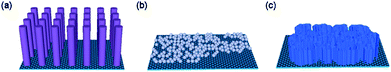 | ||
| Fig. 1 Schematics illustrating three types of graphene-based hybrid nanostructures: (a) 1D–2D, (b) 0D–2D, and (b) 2D–2D hybrid heterostructures. | ||
In addition to the 1D–2D hybrid structures, zero-dimensional (0D) inorganic nanoparticles grown on graphene layers can be categorized as 0D–2D hybrid heterostructures (Fig. 1(b)).18,19 Semiconducting quantum dots and metal oxide nanoparticles deposited on an underlying graphene sheet are useful for improving the photocatalytic functions and charge transport efficiency in many device applications, including solar cells20 and Li ion batteries.21 Finding better methods to produce 0D–2D hybrid nanostructures and understanding the photo- or charge-induced interactions through the interface between nanoparticles and graphene is a key feature of current research.
Vertical 2D inorganic nanowalls grown on graphene layers provide another kind of hybrid heterostructure (Fig. 1(c)).22 Compared with the 1D and 0D nanostructures, vertical 2D nanostructures, such as nanowalls, have rarely been studied presumably because it is difficult to control the shape and the position of the nanowalls. Nevertheless, 2D nanostructures have unique characteristics, including large surface area, shape diversity, and ease of manipulation for nanodevice applications.23 Accordingly, vertically grown nanowalls can be useful for applications in many nanodevices, including biological and chemical reservoirs and sensors, and various photonic and electronic devices.
This article reviews recent research activities on the preparation methods and characteristics of the inorganic nanostructures grown on graphene layers and their device applications. The next section briefly introduces the synthesis of graphene layers and their physical characteristics. Then, the hybrid heterostructures, inorganic nanostructures grown on graphene layers, and their device applications are reviewed. This main section is organized into four subsections including growth methods of 0D, 1D, and 2D nanostructures on graphene layers and their device applications. In particular, we focus our discussions on the growth of ZnO nanostructures on graphene layers and diverse device applications.
2. Synthesis of graphene layers and their characteristics
On the basis that graphite consists of weakly bonded graphene sheets, the top-down approach that essentially breaks a larger structure into smaller pieces can be used for graphene preparation.24 One representative top-down method is the mechanical exfoliation of graphite, in which sticky tape is first used to repeatedly split the highly ordered pyrolytic graphite (HOPG) crystals into atomically thin graphene layers.24–26 Other methods include unzipping of multiwalled carbon nanotubes (CNTs) viaetching for the fabrication of nanoribbons,27,28 and chemical oxidation of graphite to graphite oxide to obtain mildly oxidized graphene.29–31 Chemical exfoliation of graphite in a solvent combines nitric acid oxidation and small ion intercalation within graphene sheets.Peculiar and outstanding properties of monolayer graphene, including a remarkably high electron mobility (in excess of 15![[thin space (1/6-em)]](https://www.rsc.org/images/entities/char_2009.gif) 000 cm2 V−1s−1 even at room temperature) and half-integer quantum Hall effect, were first demonstrated by Andre Geim et al.32 and Philip Kim et al.33 These findings triggered enormous interest in fundamental and applied research related to graphene. In addition to the electrical properties of graphene, its mechanical properties, including the Young's modulus and fracture strength, have been investigated using an atomic force microscope (AFM).34–36 The Young's modulus of monolayer graphene was studied with force–displacement34 and/or force–volume35 measurements on a strip trench and/or circular membranes, respectively. Elastic properties and intrinsic breaking strengths of a freestanding graphene monolayer were measured using AFM-based nanoindentation. The Young's modulus and fracture strength of defect-free graphene have been reported to be 1.0 TPa and 130 GPa, respectively.36 Considering the optical characteristics of graphene, it was theoretically predicted that monolayer graphene would absorb a significant (πα = 2.3%) fraction of incident white light, where α, the fine-structure constant, is a fundamental physical coupling constant that characterizes the strength of an electromagnetic interaction.37,38 This was experimentally confirmed with graphene membranes prepared by micromechanical exfoliation of graphite and mounted on a metal scaffold having small apertures.38
000 cm2 V−1s−1 even at room temperature) and half-integer quantum Hall effect, were first demonstrated by Andre Geim et al.32 and Philip Kim et al.33 These findings triggered enormous interest in fundamental and applied research related to graphene. In addition to the electrical properties of graphene, its mechanical properties, including the Young's modulus and fracture strength, have been investigated using an atomic force microscope (AFM).34–36 The Young's modulus of monolayer graphene was studied with force–displacement34 and/or force–volume35 measurements on a strip trench and/or circular membranes, respectively. Elastic properties and intrinsic breaking strengths of a freestanding graphene monolayer were measured using AFM-based nanoindentation. The Young's modulus and fracture strength of defect-free graphene have been reported to be 1.0 TPa and 130 GPa, respectively.36 Considering the optical characteristics of graphene, it was theoretically predicted that monolayer graphene would absorb a significant (πα = 2.3%) fraction of incident white light, where α, the fine-structure constant, is a fundamental physical coupling constant that characterizes the strength of an electromagnetic interaction.37,38 This was experimentally confirmed with graphene membranes prepared by micromechanical exfoliation of graphite and mounted on a metal scaffold having small apertures.38
Following successful isolation of graphene flakes via mechanical and chemical exfoliation of graphite,24–26 a bottom-up approach has been employed to produce large, continuous films for practical applications. This approach included chemical routes,26,31,39Si sublimation from a single-crystal 4-H SiC(0001) surface,40,41 and chemical vapor deposition (CVD) on catalytic metals.14,15,42Growth of graphene films has been achieved at high temperature by flowing hydrocarbon vapor over single-crystal transition metal substrates such as Co,43Pt,44Ir,45Ru,46 and Ni.14,42,47 Among the many preparation methods, CVD offers an easy way to make large, continuous graphene films. In particular, Bae et al. used CVD of graphene layers on Ni and Cu substrates to prepare extremely large (30-inch-wide) graphene films as shown in Fig. 2(a) and 2(b).16
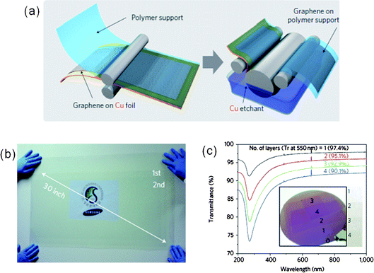 | ||
| Fig. 2 (a) Schematic of the roll-to-roll process of graphene films grown on a copper foil. (b) Ultra large-area graphene film transferred onto a 35-inch polyethylene-terephthalate (PET) substrate. (c) Transmittance spectra of layer-by-layer transferred CVD-graphene films as a function of the number of graphene layers. Inset: optical image of graphene. (Adapted from ref. 16 with permission.) | ||
The mechanism of graphene film growth by CVD has been proposed to involve dissolution of carbon in Ni at high temperature and segregation from the Ni surface during cooling of the film.42,48 Continuous graphene films can be obtained on polycrystalline Ni substrates with a pre-annealing step (at 900–1000 °C), and they exhibited a multi-domain structure with a wide variation in film thickness and in-plane orientation. A fast cooling rate of a thin Ni film with a thickness less than 200 nm has been suggested to be critical to achieve single- or few-layer graphene.14 Multi-layer graphene growth on Ni has been ascribed to C segregation or a precipitation process.48 However, high-quality graphene films with a uniform thickness profile were synthesized using a Cu foil.49 It was suggested that formation of single-layer graphene using a Cu substrate, is related to the low solubility of C atoms on a Cu surface.
CVD-grown graphene films exhibit quite good optical and electrical characteristics. In fact, the optical characteristics of CVD-grown films after transfer to glass substrates were very similar to those of mechanically exfoliated graphene with some differences due to defects or wrinkles.6 As shown in Fig. 2(c), single or multiple-layer graphene sheets still exhibit high transparency for visible light, with optical transmittance exceeding 90%, but only if the number of graphene layers is fewer than four.16,50 This relatively high optical transmittance, together with a low sheet resistance of ∼30 Ω/square16 makes graphene films a strong candidate for transparent conducting electrodes. Additionally, the carrier mobility of graphene layers grown by CVD was estimated to be ∼4050 cm2 V−1s−1 near the Dirac point,51 slightly lower than that of mechanically exfoliated graphene but much higher than electron mobility of the strained Si (∼2600 cm2 V−1s−1).52
3. Hybrid inorganic nanostructures with graphene layers
Graphene-based hybrid heterostructures with inorganic nanomaterials provide a link between solid-state nanostructures and 2D molecular science. The growth of inorganic nanocrystals on graphene layers is particularly interesting because nanostructures such as nanoparticles, nanoneedles, nanorods, and nanowalls can offer additional functionality to graphene in advanced electronics and optoelectronics. For example, CNT and inorganic nanoneedles grown on graphene layers are good candidates for field emission emitters because of their sharp tips, high aspect ratio, and high thermal and mechanical stability.53,54 Accordingly, because of the excellent electrical and thermal characteristics of graphene layers, growing inorganic nanostructures on graphene layers enables novel physical properties to be exploited in diverse, sophisticated device applications as will be discussed.3.1. Growth of 1D nanostructures on graphene layers
In this subsection, we will focus on 1D–2D nanostructure-graphene hybrids with systematically designed hybrid geometries and synthetic strategies. The typical 1D–2D hybrid is achieved by growing 1D nanostructures on a 2D graphene layer in a preferred orientation. In particular, a vertical array of 1D inorganic nanostructures can exhibit unique electrical, optical, and mechanical characteristics, properties useful in future electronic and optoelectronic applications, which eventually may allow its implementation in a 3-dimensionally integrated device platform, highly desirable for many device applications.Among inorganic semiconductors, ZnO nanostructures haven been widely studied because of their easy vertical formation.2,55Fig. 3 shows ZnO nanostructures grown on few-layer graphene layers using catalyst-free metal–organic vapor-phase epitaxy (MOVPE).22 After the graphene layers were prepared by mechanical exfoliation, ZnO nanostructures were grown using MOVPE with the reactants of diethylzinc (DEZn) and oxygen. To prevent oxidation of the graphene layers, DEZn was introduced into the reactor prior to oxygen. As shown in Fig. 3(a), straight ZnO nanoneedles grew on the graphene layers with good vertical alignment. The ZnO nanoneedles grown on graphene layers at 750 °C for 1 h had a typical density of 5 × 107 cm−2 and length of 3.5 ± 0.5 μm, while ZnO nanoneedles grown on SiO2/Si substrate under identical growth conditions had a higher density of 5 × 108 cm−2 and a longer mean length of 5.5 ± 0.8 μm. The lower density and shorter lengths of the ZnO nanoneedles on the graphene layers resulted from reduced ZnO nucleation on the graphene layers, presumably due to a large lattice constant misfit between ZnO and graphene.22
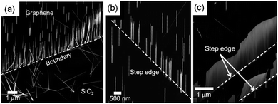 | ||
| Fig. 3 (a) SEM image of vertically aligned ZnO nanorods grown on graphene layers prepared on a SiO2/Si substrate. (b, c) SEM images of ZnO nanostructures near the step edges of graphene. (Adapted from ref. 22 with permission.) | ||
ZnO nanostructure growth behavior at the step edges and boundaries of graphene layers is very interesting. Fig. 3(b) and 3(c) show various surface morphologies for ZnO nanostructures grown on graphene layers: ZnO nanoneedles were generally located randomly, but some of them were aligned in a row as indicated by the dotted line, and vertically aligned nanowalls were also formed.22 This growth behavior could be explained in terms of enhanced nucleation and growth rates on graphene step edges that were formed during the process of transferring graphene layers from graphite onto a substrate. The step edges can serve as nucleation centers for nanoneedle and nanowall growths because nucleation and crystal growth on a step edge are favored over nucleation and growth on a terrace. Nucleation and crystal growth are further enhanced at a kink in step edges and boundaries with a high density of kinks, along which ZnO nanoneedles or nanowalls are grown.
It is noted that photoluminescence (PL) spectra of the ZnO nanostructures on graphene layers exhibited a free exciton PL peak with no carbon-related defect peak.56 This strongly suggests that high-quality ZnO nanostructures were grown on the graphene layers without deterioration of the graphene layers during MOVPE.
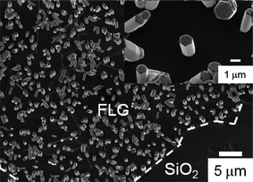
Thermal CVD using zinc powder and oxygen gas as reactants was also employed to grow ZnO nanostructures on CVD-grown graphene films.57 The morphologies and the number densities of ZnO nanostructures varied widely depending on the growth temperature in the range of 450–650 °C: as the growth temperature increased, the morphology changed from nanorods to nanoneedles with the density decreasing and the aspect ratio gradually increasing. Such a low nanorod density at high temperature could be explained by a suppressed nucleation rate on the graphene surface.22 Similar to graphene layers prepared by mechanical exfoliation, the growth of ZnO nanostructures on the multilayer graphene films synthesized by CVD was also enhanced at boundaries, such as ripples.22,57
In addition to CVD, a hydrothermal growth method was used to produce ZnO nanorods on graphene layers.58ZnO nanorods with different aspect ratios were grown on few-layer graphene sheets mounted on an SiO2/Si substrate surface by varying the growth temperature and molar concentrations. As shown in Fig. 4, ZnO nanorods with the [0001] orientation formed only on the graphene surface and not on the bare SiO2/Si substrate, indicating enhanced nucleation of ZnO on graphene layers. The spatial distribution of ZnO nanorods was homogeneous on graphene. This seems to be inconsistent with the previous result shown in Fig. 3 that ZnO nanostructures were found preferentially along the graphene step edges. The different growth behavior may result from the different synthesis methods and growth parameters used for each experiment. For example, the growth temperature in the MOCVD method is sufficiently high, so that reactant gas molecules have large kinetic energy and chemical activity. Those hot molecules are more likely to be trapped on the step edges where a higher gain in surface energy is obtained.
 | ||
| Fig. 4 SEM image of ZnO nanostructures on few-layer graphene grown using the hydrothermal method; the solution of 50 mM zinc nitrate and 50 mM hexamethylenetetramine was kept at 80 °C for 4 h. Inset: ZnO nanostructures grew only on graphene sheets, no ZnO grew on the SiO2 region. (Adapted from ref. 58 with permission.) | ||
Lee et al. adopted a similar approach to synthesize ZnO nanorod–graphene hybrid structures, except using a ZnO seed layer.59 Thus, the morphologies of nanostructures depended on the crystallinity of the ZnO seed layer, showing flower-like ZnO nanorod bundles where the ZnO nanorods were close-packed and oriented in the radial direction (Fig. 5(a)) or vertically-aligned, hexagonal-faceted ZnO nanorods (Fig. 5(b)). Additionally, regular array of ZnO nanorods were grown on the hole-patterned graphene film or a ZnO seed layer.
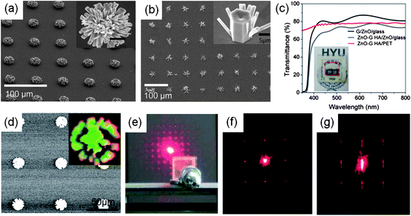 | ||
| Fig. 5 (a, b) SEM images of a ZnO nanorod–graphene hybrid structures on textured ZnO layer (a) and ZnO epilayer as seeding layers (b). (c) Optical transmittance spectra of the ZnO nanorod–graphene hybrid structure on the ZnO coated glass substrate. Inset: photograph of the hybrid structure. (d) Cathodoluminescence image of the hybrid structure showing distinct light emission from the array of ZnO nanorods (inset). (e) Photograph of the experimental setup to study the optical diffraction of a ZnO nanorod–graphene hybrid structure. Up to five orders of diffraction spots are clearly observed. (f, g) Optical diffraction patterns for the hybrid structure on a plastic substrate before bending (f) and after bending (g) down to a radius curvature of 4 mm. (Adapted from ref. 59 with permission.) | ||
The hybrid structure enables the construction of 3D nanostructures and the creation of multi-functionalities, ensuring a wide spectrum of applications.59 In particular, the hybrid structures exhibited outstanding electrical conductivity and optical transparency, comparable to those of graphene (Fig. 5(c)) as well as new optical functions such as ultraviolet (UV) light emission inherited from the ZnO nanorods (Fig. 5(d)). Meanwhile, light scattering by the ordered array of ZnO nanorods on transparent graphene yielded optical diffraction patterns with an incident laser beam, where light interaction viaZnO nanostructures can increase the coupling factor of light into and out of the active region of optoelectronic devices (Fig. 5(e)). Additionally, the excellent mechanical characteristics of graphene layers offer mechanical flexibility and structural stability at a bending radius down to ∼4 mm (Fig. 5(f) and (g)).
The position and orientation control of vertical 1D nanostructures has been of great importance for many device applications.60–63 Choi et al. produced ZnO nanorod arrays on SiO2/Si substrates using graphene as a buffer layer.64 After graphene was synthesized with a Ni film as a catalyst, then, ZnO nanorods were grown on graphene layers transferred on SiO2/Si substrates using an aqueous solution method at 90 °C for 90 min. Vertically aligned ZnO nanorods formed a dense array and showed [0001] c-axis orientation. They also used a patterned graphene layer for ZnO nanorod growth, finding that ZnO nanorods grew more densely on the graphene layer than on the exposed underlying SiO2 surface.64
First-principle computation analysis was used to investigate the stress-related energy differences between Zn–C bonds and Zn–O bonds for graphene and SiO2 surfaces, respectively. According to this calculation, ZnO nanorods on graphene were mechanically more stable than those on amorphous SiO2, resulting from stronger interactions at the heterointerface between ZnO and graphene. The mechanical stability of ZnO nanorods on graphene was tested; after ultrasonication, ZnO nanorods grown on the SiO2 surface were removed, while those on the graphene layer remained intact.
Regarding the growth of other inorganic 1D nanostructures on graphene, Yoon et al. have reported that single-crystalline Co5Ge7 nanorods with vertical alignment are grown on a very thin HOPG layer as shown in Fig. 6(a).65 A good epitaxial relation between the (100) plane of Co5Ge7 and the hexagonal basal plane of HOPG is shown; the c-axis lattice constant of Co5Ge7 (c = 5.814 Å) is quite close to four times the nearest-neighbor C–C distance of hexagonal basal plane of HOPG (4 × d = 4 × 1.421 Å = 5.684 Å), while the b-axis lattice constant of Co5Ge7 (b = 7.641 Å) is about three times the a-axis lattice constant of HOPG (3 × a = 3 × 2.46 Å = 7.38 Å). Additionally, step edges of graphene layers affect the position and morphology of the nanostructures. As shown in Fig. 6(b) and 6(c), Co5Ge7 nanobelts were formed on the step edges of graphene layers, similar to the ZnO nanoneedle growth behavior. This observation suggests that step edges of graphene serve as nucleation centers for nanocrystal growth, thereby providing an opportunity to control the position and morphology of nanocrystals on graphene.
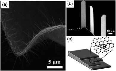 | ||
| Fig. 6 (a) SEM image of vertically aligned Co5Ge7 nanowires grown on the curved HOPG. (b) High-magnification SEM image of vertical Co5Ge7 nanobelts grown along the step edges of graphene. (c) Schematic illustration of a graphite sheet showing armchair (solid line) and zigzag (dashed line) edges. (Adapted from ref. 65 with permission.) | ||
In addition to inorganic 1D nanostructures, CNTs were prepared on reduced graphene oxide (RGO) films.53 As illustrated in Fig. 7(a), graphene oxide platelets were spin-coated onto a thermally oxidized silicon wafer from aqueous colloidal suspensions, and thermally reduced to provide good electrical conductivity. The RGO films were then decorated with patterned catalyst particles by the block-copolymer lithography method. Finally, as shown in Fig. 7(b), vertically aligned CNTs were grown by plasma-enhanced CVD at high temperature of 600 °C, forming an electrically conductive carbon hybrid film. It could be detached from the mother substrates by selectively etching the underlying sacrificial layers (in this case, the SiO2 layer was etched by HF solution), yielding a free-standing film readily transferable onto arbitrary substrates. In addition, as shown in Fig. 7(c), the transferred hybrid film exhibit unusually high mechanical strength and elasticity. Interestingly, these carbon hybrid films have Ohmic electrical contacts throughout the junctions in the CNT/metal-catalyst/“graphene film” system, potentially useful for field emission displays (FEDs).12,66 The integration of these hybrids into flexible FEDs with excellent field emission performance will be described in the next section.
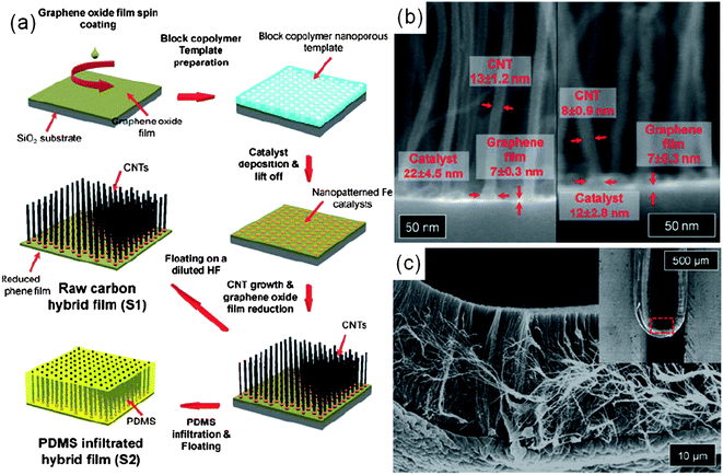 | ||
| Fig. 7 (a) Schematic illustration of the fabrication process for a carbon hybrid film. (b) Cross-sectional SEM images of a carbon hybrid film. (c) High- and low-(inset) magnification SEM images of a carbon hybrid film on a PET film bent inward. (Adapted from ref. 53 with permission.) | ||
3.2. Device applications of 1D nanostructures grown on graphene layers
Vertical 1D nanostructure arrays grown on 2D graphene layers open up a new route to construct hybrid 3D architectures for various electronic and optoelectronic device applications. The hybrid 3D nanoarchitectures have several potential advantages for device applications. First, the combination of 1D nanostructure arrays and very thin 2D graphene layers offers the significant opportunity to build a new type of graphene-based devices (e.g., LEDs,10,67 photodetectors,68 FEDs,12,53,54,66,69 piezoelectric devices,11,70 and electrical gas sensors71) by exploiting the added functionalities of the 1D nanostructures; Second, graphene-based hybrid nanostructures have higher stability to mechanical deformation associated with bending, tensile, and compressive forces (Fig. 8) because of the excellent mechanical properties of graphene itself and very small contact areas between the nanostructures and the graphene surface.11 Third, hybrid nanostructures on graphene can be transferred onto arbitrary substrates such as glass, metal, or plastic. When integrated onto flexible plastic substrates, for example, the hybrid structure can effectively relieve the strain at the heterointerface and thereby accommodate flexural deformation. These features make them very promising for soft (flexible and stretchable) electronics and optoelectronics.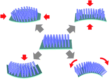 | ||
| Fig. 8 Schematic illustrating mechanical deformation of 1D–2D hybrids associated with bending, tensile, and compressive forces. | ||
Among various 1D nanostructures, direct-band-gap semiconductor nanostructures grown on graphene layers can exploit high radiative recombination rate and carrier mobility in semiconductor nanostructures, such as ZnO and GaN. The combined optical and electrical properties can be used to fabricate various optoelectronic devices, including photodetectors,68 solar cells,72 and LEDs.10 Recently, Chang et al. attempted to make UV-active graphene structures by growing ZnO nanorods directly on the graphene surface in solution.68 Using the combined effects of photosensitive ZnO nanorods and highly conductive graphene, the hybrid UV detector showed a significantly higher sensitivity of photocurrent under UV illumination than that from a single-component, graphene-based detector and little response to visible light radiation, indicating UV range selectivity.
In addition to the device applications of homogeneous 1D nanostructures, semiconductor nanorod heterostructures grown on graphene layers enabled the fabrication of flexible inorganic LEDs. Lee et al. demonstrated a method for fabricating flexible LEDs using GaN/ZnO coaxial nanorod heterostructures grown on graphene films.13 Initially, low-density ZnO nanorods were grown directly on CVD-grown graphene films. Then, high-quality coaxial nanostructure LEDs were fabricated by the heteroepitaxial coating of n-GaN, InxGa1–xN/GaN multiple-quantum-wells and p-GaN layers over the entire surface of the ZnO nanorods.73 The nanostructure LEDs exhibited strong blue light emission that could be observed with the unaided eye even under room illumination. Furthermore, the LEDs fabricated on graphene films were readily transferred onto flexible plastic substrates, demonstrating reliable operation in a flexible form and showing no significant degradation in their electroluminescent or electrical characteristics.13
Because the piezoelectric property of ZnO nanocrystals can generate electricity, many ZnO nanomaterials have been studied for generator applications.74 Recently, Choi et al. have reported a fully rollable nanogenerator using ZnO nanorods grown on graphene layers.11 As schematically shown in Fig. 9(a), graphene films were used for both the bottom and top electrodes of the generators, making it possible to produce current reproducibly over many cycles of mechanical bending or rolling (Fig. 9(b)). ZnO nanorods in the devices generate the current under mechanical deformation and the graphene sheets offer remarkably good mechanical strength and reproducible current output. This example shows how the electrical and mechanical properties of 1D–2D hybrid nanostructures can be used to fabricate 3D devices with enhanced performance.
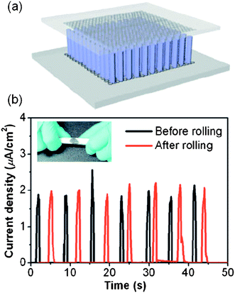 | ||
| Fig. 9 (a) Schematic illustration of a graphene-based nanogenerator. (b) Output current density before (black line) and after (red line) rolling of the graphene-based nanogenerators. (Adapted from ref. 11 with permission.) | ||
Vertical 1D nanostructures grown on conducting substrates offer stimulating opportunities for FEDs because all field emission sources rely on field enhancement due to their sharp tips or protrusions. Electron field emission from 1D nanostructures, including CNTs and inorganic semiconductor nanostructures,62,75–78 has been studied extensively. The previous research on FEDs has been performed mostly on thick and rigid substrates,62,75–77 presumably due to the high temperature preparation of the CNTs and inorganic nanostructures. On the other hand, vertically aligned CNTs have been grown on graphene substrates for the flexible FED applications.12,53,66 As shown in Fig. 10, the carbon hybrid films demonstrated excellent field emission properties even under highly deformed states,12 because of robust mechanical and electrical contacts between graphene and CNTs. Because graphene has a similar work function to that of CNTs,53 good Ohmic contacts at the junctions between CNTs and graphene can be formed easily, permitting efficient and high electrical current injection to the CNT tips through the junctions.
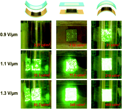 | ||
| Fig. 10 Photographs and corresponding luminance values of carbon hybrid field emission with concave, flat, and convex morphologies. (Adapted from ref. 12 with permission.) | ||
Flexible FEDs were also fabricated using ZnO nanowires grown on a RGO film substrate.54 For FED applications, ZnO nanowires were grown on the substrate using a hydrothermal method. The flexible LEDs exhibited good electron emission characteristics, resulting from good Ohmic contacts between ZnO nanowires and metallic graphene layers.54 Additionally, the hybrid structures were mechanically stable in a flexible form.
Another example of a flexible device application using the 1D nanostructures grown on graphene layers is a flexible gas sensor. With sensitivity to gas molecules and extremely large surface area, various 1D nanostructures on graphene layers can be exploited to fabricate highly sensitive, flexible gas sensors. For example, NO2 gas sensors were developed using CNTs prepared on RGO films by a plasma-enhanced CVD (PECVD) method.71 Vertical CNT arrays were grown on iron-catalyzed graphene oxide films which were spin-coated on a SiO2/Si substrate. Then, the CNTs on RGO films were transferred on to a flexible Au-coated polyimide substrate for gas sensing device applications. The transferred CNT films exhibited remarkably high sensitivity to NO2 gas with the detection limit of NO2 concentration down to 0.5 ppm. Flexible hybrid sensors also retained their gas sensing ability even under extreme bending. Other inorganic 1D nanostructures including metal oxides can also be used for fabricating highly sensitive, flexible gas sensors.79
3.3. Nanoparticles grown on graphene layers and their device applications
Many kinds of inorganic nanoparticles have been grown on graphene layers. Most inorganic nanoparticles can be produced from solution, yielding a high production rate. As one of the examples for inorganic nanocrystals on graphene layers, a CdSe quantum dot array was prepared on the basal plane of a graphene sheet using an electrochemical synthesis method.80Fig. 11(a) shows the schematic illustration of the fabrication method, where a mesoporous silica film was employed as a hexagonal-lattice mask for the selective formation of the nanocrystals. Because CdSe was deposited only through the vertical pore channels under a constant potential of −0.7 V, the hexagonal array of CdSe nanocrystals was formed on graphene layers as shown in Fig. 11(b) and 11(c). The resulting CdSe-deposited graphene sheet showed red-shifted Raman peaks in the G and 2D bands, indicating n-type doping of graphene. In addition, the large shift of Raman peaks suggests a strong interfacial charge coupling between CdSe nanocrystals and the graphene sheet.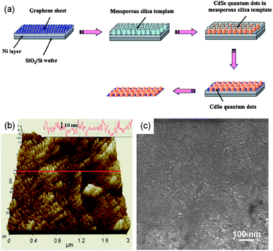 | ||
| Fig. 11 (a) Schematic procedure to synthesize a CdSe quantum dot array on the basal plane of a graphene sheet using a mesoporous silica thin film as a template. (b) AFM and (c) SEM images of a CdSe quantum dot array grown on a graphene sheet. (Adapted from ref. 79 with permission.) | ||
CdSe
nanoparticles on graphene layers can be used for quantum dot sensitized solar cell applications.20 In this study, CdSe nanoparticles were deposited onto graphene oxide layers by soaking the graphene oxide with Cd and Se precursor solutions consecutively. The amount of deposited CdSe nanoparticles was varied by controlling the weight ratio of graphene to CdSe. According to the photovoltaic measurements of the quantum dot sensitized solar cell, an optimal weight ratio of CdSe to graphene was found to be 4.5:1. It has been suggested that graphene plays an enhanced role in capturing and carrying photoinduced electrons by the CdSe nanoparticles. Other factors determining the solar cell performance may include nanoparticle size, resistance between CdSe–graphene film and the substrate, and choice of electrolyte.
In addition to II–VI compound semiconductor nanoparticles, many kinds of metal oxide nanoparticles have been grown on graphene layers. As a representative photocatalytic material, TiO2 nanocrystals were prepared on graphene oxide sheets for photocatalyst applications using a two-step method of TiO2 coating by hydrolysis and subsequent hydrothermal crystallization.81 The TiO2 and graphene oxide hybrid structures showed strong interactions between nanocrystals and graphene sheets. As a result, the photocatalytic activity was three times higher than that of the commercial TiO2 catalyst P25 (Degussa).
As for a high-capacity anode material in Li-ion batteries, transition metal oxides particles,82 such as Co3O4,83,84Fe3O4,85NiO,86 and Mn3O487nanoparticles, have been widely studied as promising alternative to graphite due to more efficient diffusion of Li ion and high specific capacities. Currently, the use of these nanostructured electrode materials is frustrated by high reactivity and mechanical degradation caused by large volume swing associated with intercalation/deintercalation of Li-ions during charge/discharge cycling.88,89 To overcome these problems, graphene or RGO sheets have been suggested as current collectors and mechanical supporters to host active nanomaterials by exploiting its high conductivity, large surface area, flexibility, and chemical stability.90–92
Encouraged by this idea, Zhu et al. has recently attempted to synthesis high lithium storage capacity by using several metal oxide–RGO hybrids.84CoO/RGO hybrid was one of the examples for high specific charge capacitances. In this work, to fabricate the hybrids, ultrathin CoO nanowalls were attached on RGO sheets, which derived from α-Co(OH)2/RGO precursors by hydrothermal process. Through the optimization of the grain size of CoO nanoparticles by annealing under different gas environments and temperature, the CoO/RGO hybrid anode materials showed very promising performance with a high specific capacity of ∼730 mAh g−1 even after 100 cycles at a discharge current density of 150 mA g−1.
TiO2–graphene hybrid nanomaterials have also been investigated as Li-ion battery anodes. For instance, self-assembled nanocrystalline TiO2 was grown on graphene in the presence of anionic sulfate surfactants using a hydrothermal synthesis method.21 Compared with that of pure TiO2, the specific capacity of the TiO2–graphene hybrid nanomaterials was more than twice higher, even at high charge and discharge rates. This suggests that graphene provides enhancement in electrically connected channels and embedded metal-oxide supporting layers.
In addition, Wang et al. reported that hybrid materials of Mn3O4 nanoparticles on RGO sheets provide an unprecedented high capacity (∼900 mAh g−1 based on the total mass of Mn3O4), good rate capability, and cycling stability.87 Although electrically insulating properties of Mn3O4 generally limit their use as an anode material, the Mn3O4 particles in the hybrid structure are electrically wired to underlying graphene layers, thereby increasing the capacity of Mn3O4 relative to its theoretical value of ∼936 mAh g−1. Meanwhile, the charging capacity was reduced three-fold in the absence of the graphene layers, indicating enhanced charge transport due to close interactions between the Mn3O4 nanoparticles and the supporting graphene layers.
Besides semiconductor quantum dots and metal oxide nanoparticles, various metal particles, such as Ag,93,94Au,95Pd,96,97 and Pt98,99nanoparticles, were also synthesized on graphene layers for many applications, including catalysis, light energy conversion, biosensor, and fuel cells. For example, Ag nanoparticles were grown by heating the RGO substrate in aqueous silver nitrate solution under N2 without using any surfactant or reducing agent.93 Additionally, the graphene–Ag composite film was also obtained through the silver mirror reaction on graphene oxide layers.94 The resulting Ag nanoparticles on graphene layers show a high optical reflectivity, and a surface-enhanced Raman scattering activity leading to the signal increase of the graphene vibration modes.
A graphene–Au nanoparticles system was also demonstrated.95Au nanoparticles were decorated on the surface of octadecylamine functionalized graphene suspended in a water-miscible organic solvent (THF). It was found that the presence of graphene sheets can prevent the Au nanoparticles from aggregating, and Au nanoparticles were attached on the surface of graphene by physisorption without any chemical bonds. The surface plasmon effect from Au nanoparticles remains largely unaffected by the underlying graphene, and thus the metal–graphene composite materials may find potential uses in plasmonic and optoelectronic devices. In addition to Ag and Au nanoparticles, other catalytic metals such as Pd, Pt, and magnetic particles can be immobilized on graphene sheet that may be useful in sensor, battery, solar cell, and fuel cell applications.18
3.4. Nanowalls grown on graphene layers and their device applications
In addition to various 0D and 1D nanostructures, vertical 2D inorganic nanowalls were grown on graphene layers,10,70 creating yet another kind of hybrid heterostructure for fabricating optoelectronic devices. As previously discussed in Sec. 3.1, for example, ZnO nanowalls as well as nanorods can be formed preferentially along the step edges or boundaries that naturally exist on graphene layers, resulting presumably from the higher surface energy at the edges and boundaries than that on the basal plane. Using this finding of enhanced nucleation and growth at the step edges, high-density ZnO nanowalls were grown on the rough graphene surface obtained by creating the artificial step edges using oxygen plasma treatment as shown in Fig. 12(a).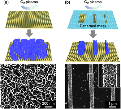 | ||
| Fig. 12 Schematic illustrations and corresponding SEM images of (a) ZnO nanowalls grown on oxygen-plasma-treated graphene layers and (b) selectively-grown ZnO nanowalls on graphene layers. | ||
Furthermore, selective-area growth of ZnO nanowalls was achieved by patterning a polymer mask layer on graphene layers and subsequently exposing it to oxygen plasma.100 As shown in Fig. 12(b), high-density ZnO nanowalls formed inside the patterned area due to the enhanced growth at the large number of step edges created by the oxygen plasma, while ZnO nanostructures rarely grew on the bare graphene surface that had not been exposed to the oxygen plasma. This suggests that graphene layers with artificially formed step edges show great promise as a substrate for selective growth of nanostructures.
High-density ZnO nanowalls grown on graphene layers have been used for fabrication of transferable LEDs by Chung et al.10 A mirror-smooth, epitaxial GaN thin film is difficult to achieve on pristine graphene layers, presumably because of the lack of chemical reactivity. In this approach, as schematically shown in Fig. 13(a), the difficulty of growing high-quality, epitaxial GaN layers on graphene layers was solved using high-density, vertically aligned ZnO nanowalls as an intermediate layer. As mentioned in Sec. 3.1, ZnO nanowalls grew epitaxially with preferred orientation along the [0001] direction on the graphene surface, which were then used as a buffer layer for epitaxial GaN growth. A flat GaN film was obtained on ZnO nanowalls grown on graphene layers by means of lateral overgrowth as shown in Fig. 13(b). These hybrid structures could be readily transferred onto foreign substrates, such as glass, metal, or plastic because they are robust enough for mechanical lift-off and transfer onto any rigid or flexible substrates. As shown in Fig. 13(c), even after transfer onto other substrates, the LEDs exhibited strong light emission comparable to that of the as-fabricated LEDs.
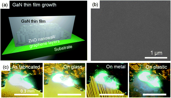 | ||
| Fig. 13 (a) Schematic illustration and (b) a SEM image of epitaxial GaN thin films on ZnO-coated graphene layers. (c) Optical images of light emissions from the as-fabricated LED on the original substrate and transferred LEDs on the foreign metal, glass, and plastic substrates. | ||
4. Conclusions
In this article, we have reviewed the recent research progress on the fabrication of hybrid inorganic nanostructures on graphene-based 2D layers in the context of an emerging material and potential device applications. Various types of graphene-based hybrid inorganic nanostructures can be built. Based on the dimensionalities of the nanostructures grown on graphene layers, they were categorized into three distinct subgroups: (i) 1D–2D hybrids such as nanorods, nanoneedles, and nanotubes; (ii) 0D–2D such as nanoparticles; and (iii) 2D–2D hybrids such as nanowalls. These hybrid heterostructures provide significant opportunities to fabricate various electronic and optoelectronic devices. Those discussed in this paper are only a preview because the full potential of hybrid nanostructures has yet to be determined.Hence, we would like to conclude this review with discussions on current challenges and following research directions toward the design and synthesis of graphene-based hybrid nanostructures for diverse applications. Although recent research on the growth of inorganic nanostructures on graphene layers has shown the feasibility for fabricating various nanodevices, including flexible devices, several important challenges still remain. First, the growth mechanism of nanostructures on many different kinds of graphene-based materials has to be investigated, which would increase controllability in the morphology and chemical and physical properties of nanostructures. In particular, uniform and homogeneous growth of nanostructures on large graphene films would be very crucial for the practical use of graphene-based hybrid inorganic nanostructures. Based on those things, second, a site-specific growth of the nanostructures is required for integrated device fabrication. Although there are several attempts to achieve selective growth, more reliable and reproducible position controls are required for practical device applications. Third, the ability to fabricate artificially designed nanomaterial heterostructures must be achieved for fabrication of more sophisticated devices with greatly enhanced performance and increased functionality. Finally, beyond single-level hybrid systems, multi-level hybrid nanostructures, which can be achieved by stacking of graphene–nanostructure hybrids, may provide new insight into the development of novel 3D nanoarchitectures with versatile and extraordinary properties. As the simplest example, a sandwich hybrid structure, composed of the graphene–nanostructure–graphene, may be useful for fabricating flexible and stretchable devices able to endure extreme deformation.
Acknowledgements
This work was financially supported by the National Creative Research Initiative Project (grant R16-2004-004-01001-0) of the Korea Science and Engineering Foundations (KOSEF). W.I.P acknowledges support from Basic Science Research Program through the National Research Foundation of Korea (NRF) funded by the Ministry of Education, Science and Technology (MEST) (2009-0071357).References
- Y. N. Xia, P. D. Yang, Y. G. Sun, Y. Y. Wu, B. Mayers, B. Gates, Y. D. Yin, F. Kim and Y. Q. Yan, Adv. Mater., 2003, 15, 353 CrossRef CAS.
- G.-C. Yi, C. R. Wang and W. I. Park, Semicond. Sci. Technol., 2005, 20, S22 CrossRef CAS.
- C. Thelander, P. Agarwal, S. Brongersma, J. Eymery, L. F. Feiner, A. Forchel, M. Scheffler, W. Riess, B. J. Ohlsson, U. Gösele and L. Samuelson, Mater. Today, 2006, 9, 28 CrossRef CAS.
- R. X. Yan, D. Gargas and P. D. Yang, Nat. Photonics, 2009, 3, 569 CrossRef CAS.
- Z. Y. Fan, H. Razavi, J. W. Do, A. Moriwaki, O. Ergen, Y. L. Chueh, P. W. Leu, J. C. Ho, T. Takahashi, L. A. Reichertz, S. Neale, K. Yu, M. Wu, J. W. Ager and A. Javey, Nat. Mater., 2009, 8, 648 CrossRef CAS.
- A. K. Geim and K. S. Novoselov, Nat. Mater., 2007, 6, 183 CrossRef CAS.
- A. K. Geim, Science, 2009, 324, 1530 CrossRef CAS.
- F. Bonaccorso, Z. Sun, T. Hasan and A. C. Ferrari, Nat. Photonics, 2010, 4, 611 CrossRef CAS.
- Y. W. Zhu, S. Murali, W. W. Cai, X. S. Li, J. W. Suk, J. R. Potts and R. S. Ruoff, Adv. Mater., 2010, 22, 3906 CrossRef CAS.
- K. Chung, C.-H. Lee and G.-C. Yi, Science, 2010, 330, 655 CrossRef CAS.
- D. Choi, M. Y. Choi, W. M. Choi, H. J. Shin, H. K. Park, J. S. Seo, J. Park, S. M. Yoon, S. J. Chae, Y. H. Lee, S. W. Kim, J. Y. Choi, S. Y. Lee and J. M. Kim, Adv. Mater., 2010, 22, 2187 CrossRef CAS.
- D. H. Lee, J. A. Lee, W. J. Lee and S. O. Kim, Small, 2011, 7, 95 CrossRef CAS.
- C.-H. Lee, Y.-J. Kim, Y. J. Hong, S.-R. Jeon, S. Bae, B. H. Hong and G.-C. Yi, 2011, submitted.
- K. S. Kim, Y. Zhao, H. Jang, S. Y. Lee, J. M. Kim, J. H. Ahn, P. Kim, J. Y. Choi and B. H. Hong, Nature, 2009, 457, 706 CrossRef CAS.
- X. S. Li, W. W. Cai, J. H. An, S. Kim, J. Nah, D. X. Yang, R. Piner, A. Velamakanni, I. Jung, E. Tutuc, S. K. Banerjee, L. Colombo and R. S. Ruoff, Science, 2009, 324, 1312 CrossRef CAS.
- S. Bae, H. Kim, Y. Lee, X. F. Xu, J. S. Park, Y. Zheng, J. Balakrishnan, T. Lei, H. R. Kim, Y. I. Song, Y. J. Kim, K. S. Kim, B. Özyilmaz, J. H. Ahn, B. H. Hong and S. Iijima, Nat. Nanotechnol., 2010, 5, 574 CrossRef CAS.
- Y. Chujo, KONA, 2007, 25, 255 Search PubMed.
- P. V. Kamat, J. Phys. Chem. Lett., 2010, 1, 520 CrossRef CAS.
- Z. T. Luo, L. A. Somers, Y. P. Dan, T. Ly, N. J. Kybert, E. J. Mele and A. T. C. Johnson, Nano Lett., 2010, 10, 777 CrossRef CAS.
- S. R. Sun, L. A. Gao, Y. Q. Liu and J. Sun, Appl. Phys. Lett., 2011, 98, 093112 CrossRef.
- D. H. Wang, D. W. Choi, J. Li, Z. G. Yang, Z. M. Nie, R. Kou, D. H. Hu, C. M. Wang, L. V. Saraf, J. G. Zhang, I. A. Aksay and J. Liu, ACS Nano, 2009, 3, 907 CrossRef CAS.
- Y.-J. Kim, J. H. Lee and G.-C. Yi, Appl. Phys. Lett., 2009, 95, 213101 CrossRef.
- C.-H. Lee, Y.-J. Kim, J. Lee, Y. J. Hong, J. M. Jeon, M. Kim, S. Hong and G.-C. Yi, Nanotechnology, 2011, 22, 055205 CrossRef.
- K. S. Novoselov, A. K. Geim, S. V. Morozov, D. Jiang, Y. Zhang, S. V. Dubonos, I. V. Grigorieva and A. A. Firsov, Science, 2004, 306, 666 CrossRef CAS.
- X. K. Lu, M. F. Yu, H. Huang and R. S. Ruoff, Nanotechnology, 1999, 10, 269 CrossRef CAS.
- Z. H. Ni, H. M. Wang, J. Kasim, H. M. Fan, T. Yu, Y. H. Wu, Y. P. Feng and Z. X. Shen, Nano Lett., 2007, 7, 2758 CrossRef CAS.
- D. V. Kosynkin, A. L. Higginbotham, A. Sinitskii, J. R. Lomeda, A. Dimiev, B. K. Price and J. M. Tour, Nature, 2009, 458, 872 CrossRef CAS.
- L. Y. Jiao, L. Zhang, X. R. Wang, G. Diankov and H. J. Dai, Nature, 2009, 458, 877 CrossRef CAS.
- S. Stankovich, D. A. Dikin, G. H. B. Dommett, K. M. Kohlhaas, E. J. Zimney, E. A. Stach, R. D. Piner, S. T. Nguyen and R. S. Ruoff, Nature, 2006, 442, 282 CrossRef CAS.
- A. P. Yu, P. Ramesh, M. E. Itkis, E. Bekyarova and R. C. Haddon, J. Phys. Chem. C, 2007, 111, 7565 CAS.
- P. K. Ang, S. Wang, Q. L. Bao, J. T. L. Thong and K. P. Loh, ACS Nano, 2009, 3, 3587 CrossRef CAS.
- K. S. Novoselov, A. K. Geim, S. V. Morozov, D. Jiang, M. I. Katsnelson, I. V. Grigorieva, S. V. Dubonos and A. A. Firsov, Nature, 2005, 438, 197 CrossRef CAS.
- Y. B. Zhang, Y. W. Tan, H. L. Stormer and P. Kim, Nature, 2005, 438, 201 CrossRef CAS.
- I. W. Frank, D. M. Tanenbaum, A. M. Van der Zande and P. L. McEuen, J. Vac. Sci. Technol., B: Microelectron. Nanometer Struct.–Process., Meas., Phenom., 2007, 25, 2558 CrossRef CAS.
- M. Poot and H. S. J. van der Zant, Appl. Phys. Lett., 2008, 92, 063111 CrossRef.
- C. Lee, X. D. Wei, J. W. Kysar and J. Hone, Science, 2008, 321, 385 CrossRef CAS.
- K. F. Mak, M. Y. Sfeir, Y. Wu, C. H. Lui, J. A. Misewich and T. F. Heinz, Phys. Rev. Lett., 2008, 101, 196405 CrossRef.
- R. R. Nair, P. Blake, A. N. Grigorenko, K. S. Novoselov, T. J. Booth, T. Stauber, N. M. R. Peres and A. K. Geim, Science, 2008, 320, 1308 CrossRef CAS.
- A. G. Cano-Marquez, F. J. Rodriguez-Macias, J. Campos-Delgado, C. G. Espinosa-Gonzalez, F. Tristan-Lopez, D. Ramirez-Gonzalez, D. A. Cullen, D. J. Smith, M. Terrones and Y. I. Vega-Cantu, Nano Lett., 2009, 9, 1527 CrossRef CAS.
- C. Berger, Z. M. Song, X. B. Li, X. S. Wu, N. Brown, C. Naud, D. Mayou, T. B. Li, J. Hass, A. N. Marchenkov, E. H. Conrad, P. N. First and W. A. de Heer, Science, 2006, 312, 1191 CrossRef CAS.
- J. Hass, F. Varchon, J. E. Millan-Otoya, M. Sprinkle, N. Sharma, W. A. De Heer, C. Berger, P. N. First, L. Magaud and E. H. Conrad, Phys. Rev. Lett., 2008, 100, 125504 CrossRef CAS.
- A. Reina, X. T. Jia, J. Ho, D. Nezich, H. B. Son, V. Bulovic, M. S. Dresselhaus and J. Kong, Nano Lett., 2009, 9, 30 CrossRef CAS.
- A. Varykhalov and O. Rader, Phys. Rev. B: Condens. Matter Mater. Phys., 2009, 80, 035437 CrossRef.
- H. Ueta, M. Saida, C. Nakai, Y. Yamada, M. Sasaki and S. Yamamoto, Surf. Sci., 2004, 560, 183 CrossRef CAS.
- J. Coraux, A. T. N'Diaye, C. Busse and T. Michely, Nano Lett., 2008, 8, 565 CrossRef CAS.
- P. W. Sutter, J. I. Flege and E. A. Sutter, Nat. Mater., 2008, 7, 406 CrossRef CAS.
- S. S. Datta, D. R. Strachan, E. J. Mele and A. T. C. Johnson, Nano Lett., 2009, 9, 7 CrossRef CAS.
- Q. K. Yu, J. Lian, S. Siriponglert, H. Li, Y. P. Chen and S. S. Pei, Appl. Phys. Lett., 2008, 93, 113103 CrossRef.
- X. S. Li, W. W. Cai, L. Colombo and R. S. Ruoff, Nano Lett., 2009, 9, 4268 CrossRef CAS.
- X. S. Li, Y. W. Zhu, W. W. Cai, M. Borysiak, B. Y. Han, D. Chen, R. D. Piner, L. Colombo and R. S. Ruoff, Nano Lett., 2009, 9, 4359 CrossRef CAS.
- J. H. Chen, C. Jang, S. D. Xiao, M. Ishigami and M. S. Fuhrer, Nat. Nanotechnol., 2008, 3, 206 CrossRef CAS.
- S. F. Nelson, K. Ismail, J. O. Chu and B. S. Meyerson, Appl. Phys. Lett., 1993, 63, 367 CrossRef CAS.
- D. H. Lee, J. E. Kim, T. H. Han, J. W. Hwang, S. Jeon, S. Y. Choi, S. H. Hong, W. J. Lee, R. S. Ruoff and S. O. Kim, Adv. Mater., 2010, 22, 1247 CrossRef CAS.
- J. O. Hwang, D. H. Lee, J. Y. Kim, T. H. Han, B. H. Kim, M. Park, K. No and S. O. Kim, J. Mater. Chem., 2011, 21, 3432 RSC.
- W. I. Park, D. H. Kim, S. W. Jung and G.-C. Yi, Appl. Phys. Lett., 2002, 80, 4232 CrossRef CAS.
- S. T. Tan, X. W. Sun, Z. G. Yu, P. Wu, G. Q. Lo and D. L. Kwong, Appl. Phys. Lett., 2007, 91, 072101 CrossRef.
- J. A. Lin, M. Penchev, G. P. Wang, R. K. Paul, J. B. Zhong, X. Y. Jing, M. Ozkan and C. S. Ozkan, Small, 2010, 6, 2448 CrossRef CAS.
- Y.-J. Kim, Hadiyawarman, A. Yoon, M. Kim, G.-C. Yi and C. Liu, Nanotechnology, 2011, 22, 245603 CrossRef.
- J. M. Lee, Y. B. Pyun, J. Yi, J. W. Choung and W. I. Park, J. Phys. Chem. C, 2009, 113, 19134 CAS.
- Y.-J. Kim, C.-H. Lee, Y. J. Hong, G.-C. Yi, S. S. Kim and H. Cheong, Appl. Phys. Lett., 2006, 89, 163128 CrossRef.
- Y. J. Hong, S. J. An, H. S. Jung, C.-H. Lee and G.-C. Yi, Adv. Mater., 2007, 19, 4416 CrossRef CAS.
- Y. J. Hong, H. S. Jung, J. Yoo, Y.-J. Kim, C.-H. Lee, M. Kim and G.-C. Yi, Adv. Mater., 2009, 21, 222 CrossRef CAS.
- H. J. Fan, P. Werner and M. Zacharias, Small, 2006, 2, 700 CrossRef CAS.
- W. M. Choi, K.-S. Shin, H. S. Lee, D. Choi, K. Kim, H.-J. Shin, S.-M. Yoon, J.-Y. Choi and S.-W. Kim, Nano Res., 2011, 4 DOI:10.1007/s12274-011-0100-6.
- H. Yoon, K. Seo, N. Bagkar, J. In, J. Park, J. Kim and B. Kim, Adv. Mater., 2009, 21, 4979 CrossRef CAS.
- D. H. Lee, J. A. Lee, W. J. Lee, D. S. Choi and S. O. Kim, J. Phys. Chem. C, 2010, 114 Search PubMed.
- J. M. Lee, J. W. Choung, J. Yi, D. H. Lee, M. Samal, D. K. Yi, C.-H. Lee, G.-C. Yi, U. Paik, J. A. Rogers and W. I. Park, Nano Lett., 2010, 10, 2783 CrossRef CAS.
- H. X. Chang, Z. H. Sun, K. Y. F. Ho, X. M. Tao, F. Yan, W. M. Kwok and Z. J. Zheng, Nanoscale, 2011, 3, 258 RSC.
- S. Kim, H. Choi, M. Jung, S. Y. Choi and S. Ju, Nanotechnology, 2010, 21 Search PubMed.
- B. Kumar, K. Y. Lee, H.-K. Park, S. J. Chae, Y. H. Lee and S.-W. Kim, preprint:cond-mat.mtrl-sci, 2011 Search PubMed, arXiv:1102.0124v1.
- H. Y. Jeong, D. S. Lee, H. K. Choi, D. H. Lee, J. E. Kim, J. Y. Lee, W. J. Lee, S. O. Kim and S. Y. Choi, Appl. Phys. Lett., 2010, 96, 213105 CrossRef.
- Z. Y. Yin, S. X. Wu, X. Z. Zhou, X. Huang, Q. C. Zhang, F. Boey and H. Zhang, Small, 2010, 6, 307 CrossRef CAS.
- C.-H. Lee, J. Yoo, Y. J. Hong, J. Cho, Y.-J. Kim, S.-R. Jeon, J. H. Baek and G.-C. Yi, Appl. Phys. Lett., 2009, 94, 213101 CrossRef.
- Z. L. Wang and J. H. Song, Science, 2006, 312, 242 CrossRef CAS.
- W. A. Deheer, A. Chatelain and D. Ugarte, Science, 1995, 270, 1179 CAS.
- S. S. Fan, M. G. Chapline, N. R. Franklin, T. W. Tombler, A. M. Cassell and H. J. Dai, Science, 1999, 283, 512 CrossRef CAS.
- J. Yoo, W. I. Park and G.-C. Yi, J. Vac. Sci. Technol., B, 2005, 23, 1970 CAS.
- Y.-J. Kim, J. Yoo, B. H. Kwon, Y. J. Hong, C.-H. Lee and G.-C. Yi, Nanotechnology, 2008, 19, 315202 CrossRef.
- J. Yi, J. M. Lee and W. I. Park, Sens. Actuators B: Chem., 2011, 155, 264 CrossRef.
- Y.-T. Kim, J. H. Han, B. H. Hong and Y. U. Kwon, Adv. Mater., 2010, 22, 515 CrossRef CAS.
- Y. Y. Liang, H. L. Wang, H. S. Casalongue, Z. Chen and H. J. Dai, Nano Res., 2010, 3, 701 CrossRef CAS.
- J. M. Tarascon and M. Armand, Nature, 2001, 414, 359 CrossRef CAS.
- P. Poizot, S. Laruelle, S. Grugeon, L. Dupont and J. M. Tarascon, Nature, 2000, 407, 496 CrossRef CAS.
- J. X. S. Zhu, Y. K., Z. Zeng, X. Zhang, M. Srinivasan, S. Mhaisalkar, H. Zhang, H. H. Hng and Q. Y. Yan, J. Phys. Chem. C, 2011, 115, 8400 CAS.
- W. H. Shi, J. X. Zhu, D. H. Sim, Y. Y. Tay, Z. Y. Lu, X. J. Zhang, Y. Sharma, M. Srinivasan, H. Zhang, H. H. Hng and Q. Y. Yan, J. Mater. Chem., 2011, 21, 3422 RSC.
- H. L. Wang, H. S. Casalongue, Y. Y. Liang and H. J. Dai, J. Am. Chem. Soc., 2010, 132, 7472 CrossRef CAS.
- H. L. Wang, L. F. Cui, Y. A. Yang, H. S. Casalongue, J. T. Robinson, Y. Y. Liang, Y. Cui and H. J. Dai, J. Am. Chem. Soc., 2010, 132, 13978 CrossRef CAS.
- R. A. Huggins, J. Power Sources, 1999, 81–82, 13 CrossRef CAS.
- C. K. Chan, X. F. Zhang and Y. Cui, Nano Lett., 2008, 8, 307 CrossRef CAS.
- S. M. Paek, E. Yoo and I. Honma, Nano Lett., 2009, 9, 72 CrossRef CAS.
- Z. S. Wu, W. C. Ren, L. Wen, L. B. Gao, J. P. Zhao, Z. P. Chen, G. M. Zhou, F. Li and H. M. Cheng, ACS Nano, 2010, 4, 3187 CrossRef CAS.
- D. H. Wang, R. Kou, D. Choi, Z. G. Yang, Z. M. Nie, J. Li, L. V. Saraf, D. H. Hu, J. G. Zhang, G. L. Graff, J. Liu, M. A. Pope and I. A. Aksay, ACS Nano, 2010, 4, 1587 CrossRef CAS.
- X. Z. Zhou, X. Huang, X. Y. Qi, S. X. Wu, C. Xue, F. Y. C. Boey, Q. Y. Yan, P. Chen and H. Zhang, J. Phys. Chem. C, 2009, 113, 10842 CAS.
- C. Xu and X. Wang, Small, 2009, 5, 2212 CrossRef CAS.
- R. Muszynski, B. Seger and P. V. Kamat, J. Phys. Chem. C, 2008, 112, 5263 CAS.
- Y. Li, X. B. Fan, J. J. Qi, J. Y. Ji, S. L. Wang, G. L. Zhang and F. B. Zhang, Nano Res., 2010, 3, 429 CrossRef CAS.
- X. M. Chen, G. H. Wu, J. M. Chen, X. Chen, Z. X. Xie and X. R. Wang, J. Am. Chem. Soc., 2011, 133, 3693 CrossRef CAS.
- S. J. Guo, D. Wen, Y. M. Zhai, S. J. Dong and E. K. Wang, ACS Nano, 2010, 4, 3959 CrossRef CAS.
- R. S. Dey and C. R. Raj, J. Phys. Chem. C, 2010, 114, 21427 CAS.
- J.-H. Lee, Y.-J. Kim and G.-C. Yi, 2011, submitted.
| This journal is © The Royal Society of Chemistry 2011 |