Electrospinning-derived Tb2(WO4)3:Eu3+ nanowires: energy transfer and tunable luminescence properties
Zhiyao
Hou
ab,
Ziyong
Cheng
*a,
Guogang
Li
a,
Wenxin
Wang
b,
Chong
Peng
a,
Chunxia
Li
a,
Ping'an
Ma
a,
Dongmei
Yang
a,
Xiaojiao
Kang
a and
Jun
Lin
*a
aState Key Laboratory of Rare Earth Resource Utilization, Changchun Institute of Applied Chemistry, Chinese Academy of Sciences, Changchun, 130022, P. R. China. E-mail: zycheng@ciac.jl.cn; jlin@ciac.jl.cn
bKey Laboratory of Superlight Materials and surface Technology, Ministry of Education, College of Materials Science and Chemical Engineering, Harbin Engineering University, Harbin, 150001, P. R. China
First published on 15th February 2011
Abstract
One-dimensional Tb2(WO4)3 and Tb2(WO4)3:Eu3+ nanowires have been prepared by a combination method of sol–gel process and electrospinning. X-Ray diffraction (XRD), scanning electron microscopy (SEM), transmission electron microscopy (TEM), photoluminescence (PL), low voltage cathodoluminescence (CL) and time-resolved emission spectra as well as kinetic decays were used to characterize the resulting samples. The as-obtained precursor samples present fiber-like morphology with uniform size, and Tb2(WO4)3 and Tb2(WO4)3:Eu3+ nanowires were formed after annealing. Under ultraviolet excitation and low-voltage electron beams excitation into WO42−and the f–f transition of Tb3+, the Tb2(WO4)3 samples show the characteristic emission of Tb3+ corresponding to 5D4–7F6, 5, 4, 3 transitions due to an efficient energy transfer from WO42− to Tb3+, while Tb2(WO4)3:Eu3+ samples mainly exhibit the characteristic emission of Eu3+ corresponding to 5D0–7F0, 1, 2 transitions due to an energy transfer occurs from WO42− and Tb3+ to Eu3+. The increase of Eu3+ concentration leads to the increase of the energy transfer efficiency from Tb3+ to Eu3+. The PL color of Tb2(WO4)3:x mol% Eu3+ phosphors can be tuned from green to red easily by changing the doping concentration (x) of Eu3+, making the materials have potential applications in fluorescent lamps and color display fields.
1. Introduction
Inorganic phosphor materials based on rare earth (RE) compounds and RE ion-doped compounds have been widely used in the fields of high-performance luminescent devices, catalysts, and other functional materials based on their electronic, optical, and chemical characteristics arising from their 4f electrons.1 Recently, the use of phosphors represents a fast growing industry due to the wide range of applications: light-emitting diodes (LEDs), cathode ray tubes (CRTs), field emission displays (FEDs), vacuum fluorescent displays (VFDs), plasma display panels (PDPs), and X-ray imaging scintillators.2 Rare earth oxide phosphors have gained interest due to their better thermal and chemical stability as well as their environmental friendliness, which are currently used in the screens of flat-panel displays (FPDs), VFDs, and FEDs.3 Therefore, more attention has been paid to the improvement of original rare earth oxide phosphors and (or) developing new rare earth oxide phosphors materials with respect to the wide possible applications.It is well known that the energy transfer plays an important role in luminescent materials both from theoretical and practical points of view.4 It has been recognized that the luminescence intensities of various rare earth ions can be enhanced or quenched by the energy transfer from other codoped rare earth ions.4a,5 For example, the emission intensity of Tb3+ is greatly enhanced by an energy transfer from Ce3+ in LaPO4:Ce3+,Tb3+ phosphor, leading it to be an efficient luminescent material for fluorescent lamps.4a,c It has also been demonstrated that as a result of the energy transfer phenomena it is possible to reduce the threshold energy of laser oscillation in some solid laser materials.6 As the most frequently used activator ions in luminescent materials, the Eu3+ and Tb3+ mainly show emissions due to transitions of 5D0–7FJ (J = 1, 2, 3, 4) in the red region and 5D4–7FJ (J = 6, 5, 4, 3) in the green region, respectively.1c,7 Although the energy transfer phenomena between different rare earth ions have been extensively investigated, little attention has been paid to the case between Tb3+ and Eu3+, and so far the energy transfer phenomenon from Tb3+ to Eu3+ have been observed and investigated only in limited hosts.8
To obtain desired one-dimensional (1D) RE ions doped phosphors, electrospinning is intensively used because it has been developed since 1934 for the synthesis of 1D nanomaterials. Electrospinning is an effective and simple method for preparing a rich variety of materials,9 such as polymers, inorganic and hybrid (organic-inorganic) compounds. On the other hand, the sol–gel process has been proven as an efficient way to produce nanoparticles10 and nanocoatings11 of metal oxide. Sol–gel techniques can be employed to prepare precursor solutions, which have been used to deposit coatings by spinning and dipping.12 1D materials fabricated by a combination method of sol–gel process and electrospinning have become important for their exceptionally long length, uniform diameter, diverse composition and large surface areas, which can be applied in biomedical fields, reinforced composites, catalyst supports, sensors, electronic and optical devices, as well as sacrificial templates.13
Metal tungstates are an important family of inorganic material that have extensive potential applications in various fields,14 such as photoluminescence, fluorescent lamps, microwave applications, optical fibers, scintillator materials, X-ray intensified screen. Rare earth tungstates Ln2(WO4)3 (Ln = lanthanides) have been proved to be useful host lattices for the luminescence of rare earth ions.15Ln2(WO4)3 can be divided into two groups with different structures governed by the ionic radius of Ln3+: crystallising in monoclinic for Ln = La–Dy with larger size and orthorhombic for Ln = Ho–Lu with smaller sizes. To the best of our knowledge, there have been few reports about synthesis and luminescent properties of Tb2(WO4)3 and/or RE3+-doped Tb2(WO4)3 materials. Especially, there have no reports concerning the preparation of Eu3+-doped Tb2(WO4)3 1D phosphors viaelectrospinning method, and the corresponding energy transfer from WO42− and Tb3+ to Eu3+ in Tb2(WO4)3 host has not been realized and reported. Accordingly, in this paper, we report the preparation of 1D wirelike Tb2(WO4)3 and Tb2(WO4)3:Eu3+ phosphors through a combination method of sol–gel process and electrospinning, as well as their photoluminescent and cathodoluminescent properties. Moreover, we investigate the energy transfer property from WO42− and Tb3+ to Eu3+ in Tb2(WO4)3, which results in the tunable emission colors from such phosphor materials.
2. Experimental
Chemicals and materials
Polyvinylpyrrolidone (PVP, Mw = 1![[thin space (1/6-em)]](https://www.rsc.org/images/entities/char_2009.gif) 300000) was purchased from Aldrich, and ammonium (meta) tungstate hydrate (H26N6O41W12·18H2O) was purchased from Fluka. Citric acid monohydrate C6H8O7·H2O (≥99.5%, A. R.), nitric acid HNO3 (A. R.), hydrogen peroxide (≥30%, A. R.) and ethanol were all purchased from Beijing Fine Chemical Company. Tb4O7 and Eu2O3 (99.99%) were purchased from Science and Technology Parent Company of Changchun Institute of Applied Chemistry. Tb(NO3)3 and Eu(NO3)3 were prepared by dissolving Tb4O7 and Eu2O3 in dilute nitric acid HNO3 containing H2O2, and evaporating the water in the solutions by heating. All the initial chemicals in this work were used without further purification.
300000) was purchased from Aldrich, and ammonium (meta) tungstate hydrate (H26N6O41W12·18H2O) was purchased from Fluka. Citric acid monohydrate C6H8O7·H2O (≥99.5%, A. R.), nitric acid HNO3 (A. R.), hydrogen peroxide (≥30%, A. R.) and ethanol were all purchased from Beijing Fine Chemical Company. Tb4O7 and Eu2O3 (99.99%) were purchased from Science and Technology Parent Company of Changchun Institute of Applied Chemistry. Tb(NO3)3 and Eu(NO3)3 were prepared by dissolving Tb4O7 and Eu2O3 in dilute nitric acid HNO3 containing H2O2, and evaporating the water in the solutions by heating. All the initial chemicals in this work were used without further purification.
Preparation
1D Tb2(WO4)3:x mol% Eu3+ (x = 0–5) samples were prepared by a method of sol–gel process and electrospinning. The doping concertrations of Eu3+ are 0.3–5 mol % of Tb3+ in Tb2(WO4)3. The stoichiometric amounts of Tb(NO3)3, Eu(NO3)3, and H26N6O41W12·18H2O were dissolved in deionized water, then the solution was mixed with a water–ethanol solution (final volume ratio of water to ethanol is 1:4) containing citric acid as a chelating agent for the metal ions. The molar ratio of metal ions to citric acid was 1:2. A certain amount of polyvinylpyrrolidone (PVP, Mw = 1300000, Aldrich) was added to adjust the viscoelastic behavior of the solution (the weight percentage of PVP is 7% in the water–ethanol solution). The solution was stirred for 4 h to obtain a homogeneous hybrid sol for further electrospinning. The distance between the spinneret (a metallic needle) and collector (a grounded conductor) was fixed at 16 cm and the high-voltage supply was maintained at 15 kV. The spinning rate was controlled at 0.5 mL h−1 by a syringe pump (TJ-3A/W0109-1B, Baoding Longer Precision Pump Co., Ltd, China). The as-prepared hybrid precursor samples were annealed at desired temperature (800 °C) with the heating rate of 2 °C min−1 and held there for 4 h in air.
Characterization
The X-ray diffraction (XRD) patterns of the samples were carried out on a D8 Focus diffractometer (Bruker) with use of Cu KR radiation (λ = 0.15405 nm). The morphology of the samples was inspected using a field emission scanning electron microscope (Philips XL 30). The photoluminescence (PL) measurements were recorded with a Hitachi F-4500 spectrophotometer equipped with a 150 W xenon lamp as the excitation source. The cathodoluminescence (CL) measurements were conducted in an ultrahigh-vacuum chamber (<10−8 Torr), where the phosphors were excited by an electron beam at a voltage range of 23–25 kV with different filament currents 90–106 mA, and the spectra were recorded using an F-4500 spectrophotometer. The luminescence decay curves and time-resolved photoluminescence spectra were obtained from a Lecroy Wave Runner 6100 digital oscilloscope (1 GHz) using a tunable laser (pulse width = 4 ns, gate = 50 ns) as excitation (Continuum Sunlite OPO, pumped by a third harmonic of Nd:YAG, 355 nm). All the measurements were performed at room temperature.3. Results and discussion
Structure and morphology
Fig. 1 shows the XRD patterns of Tb2(WO4)3, Tb2(WO4)3:5 mol % Eu3+ annealed at 800 °C as well as the JCPDS card (No. 28–1290) for Tb2(WO4)3, respectively. Both Tb2(WO4)3 and Tb2(WO4)3:5 mol % Eu3+ exhibit very similar X-ray diffraction patterns with monoclinic structure [Fig. 1(a), (b)], so that we can expect their full miscibility. Therefore, the whole solid solution Tb2(WO4)3:x mol % Eu3+ from x = 0 to 5 is expected to form. When the Tb3+ was substituted by the Eu3+ with bigger radius, the corresponding XRD peaks shift to lower angle direction based on the Vegard law. No additional peaks of other phases have been found, indicating that Eu3+ has been effectively built into the Tb2(WO4)3 host lattice.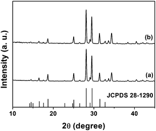 | ||
| Fig. 1 XRD patterns for Tb2(WO4)3 (a), Tb2(WO4)3:5 mol % Eu3+ (b) and the JCPDS card 28–1290 of Tb2(WO4)3 for comparison. | ||
Fig. 2 shows the SEM images of the as-formed precursor Tb2(WO4)3:5 mol % Eu3+ hybrid fibers, as well as those samples annealed at high temperature (800 °C), respectively. From the low-magnification SEM micrographs of as-formed precursor [Fig. 2(a)] and those annealed at 800 °C [Fig. 2(c)], it can be seen that the samples consist of uniform fibers with length of several tens to hundred micrometres. It also can be observed that the as-formed precursor fibers are smooth with diameters ranging from 300 to 500 nm from the high-magnification SEM micrograph [Fig. 2(b)]. After being annealed at 800 °C, the fiber diameters decrease greatly due to the decomposition of the organic species and the formation of inorganic phase. The diameters of the nanowires annealed at 800 °C for 4 h become 80 to 150 nm [Fig. 2(d)]. It should be mentioned that the key strategy of sol–gel/electrospinning method to obtain 1D inorganic nanomaterials was to form a solution with viscoelastic behavior similar to that of a conventional polymer solution. In our experiments, the purposes of controlling the volume ratio of water to alcohol and the weight percentage of PVP were to adjust the viscoelastic behavior, making the hybrid solution suitable for further electrospinning.
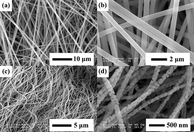 | ||
| Fig. 2 SEM images for the as-formed precursor for Tb2(WO4)3:5 mol % Eu3+ nanowires: images with low magnification (a) and high magnification (b); and those annealed at 800 °C: images with low magnification (c), high magnification (d). | ||
Photoluminescence properties
The Tb2(WO4)3 sample emits green light ultraviolet (UV) irradiation. Fig. 3 shows the excitation and emission spectra of the Tb2(WO4)3 samples. The excitation spectrum [left of Fig. 3(a) and (b)] of Tb2(WO4)3 monitored with 543 nm emission of Tb3+ (5D4–7F5) consists two main features, a broad band with maxima at 280 nm in the range of 200–330 nm, which is ascribed to the charge transfer absorption in WO42−groups in which an oxygen (O) 2p electron goes into one of the empty tungsten (W) 5d orbital, and the characteristic f–f transition lines within the Tb3+ 4f8 configuration in the longer wavelength region with maxima at 490 nm (5D4), assigned as the transitions from the 7F6 ground state to the different excited states of Tb3+, i.e., 322 nm (5D0), 345 nm (5G2), 356 nm (5D2), 363 nm (5L10), 373 nm (5G6) and 382 nm (5D3), respectively.13 The presence of the excitation peak of the WO42−groups in the excitation spectrum of Tb3+ indicates that there is an energy transfer from the WO42−groups to Tb3+ ions in the Tb2(WO4)3 nanowires. Upon excitation into WO42−group at 280 nm, the obtained emission spectrum [Fig. 3(a), right] of Tb2(WO4)3 consists of f–f transition lines within 4f8 electron configuration of Tb3+, i.e., 5D4–7F6 (488 nm) in the blue region and 5D4–7F5 (543 nm) in the green region, as well as 5D4–7F4 (585 nm), 5D4–7F3 (619 nm) in the red region. The strongest one is located at 543 nm corresponding to 5D4–7F5 transition of Tb3+. Compared with the emission of Tb3+, the intrinsic blue emission from WO42−groups is very weak, suggesting that an efficient energy transfer from WO42−groups to Tb3+ has occurred. Excitation into Tb3+ at 490 nm yields the emissions spectrum corresponding to the f–f transitions of Tb3+, which is also dominated by the green emission 5D4–7F5 transition at 543 nm [Fig. 3(b), right].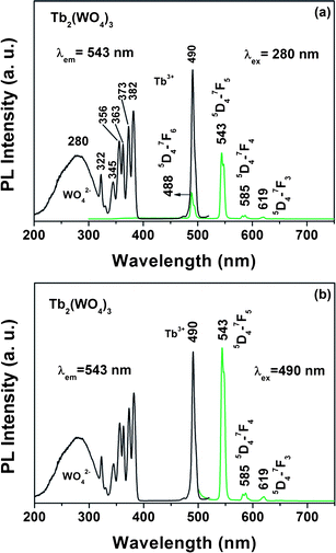 | ||
| Fig. 3 Excitation and emission spectra of the Tb2(WO4)3 upon excitation into WO42− (a) and Tb3+ (b). | ||
However, the green emission of the Tb2(WO4)3 host material changes greatly when doing Eu3+ in it. The Tb2(WO4)3:5 mol % Eu3+ sample shows a red emission under UV excitation. Fig. 4 shows the excitation and emission spectra of Tb2(WO4)3:5 mol % Eu3+ samples. The excitation spectra [left of Fig. 4] recorded at the 615 nm (5D0–7F2) of Eu3+ are composed of the excitation bands of WO42− and Tb3+, which are identical with the excitation spectrum of Tb3+ in Tb2(WO4)3 [Left of Fig. 3], except for some minor f–f transition lines within the Eu3+ 4f6 configuration (398 nm: 7F0–5L6, 420 nm: 7F0–5D3, and 468 nm: 7F0–5D2). The presence of the excitation bands and lines of WO42− and Tb3+ in the excitation spectra monitored with Eu3+ emission clearly indicates that an energy transfer has occurred from WO42− and Tb3+ to Eu3+ in the Tb2(WO4)3:5 mol % Eu3+ samples. Excitation into WO42−group at 280 nm yields mainly the emission of Eu3+ (5D0–7F1 at 592 nm, 5D0–7F2 at 615, 5D0–7F3 at 652 nm, and 5D0–7F4 at 702 nm), together with the emission of Tb3+ (488 nm at 5D4–7F6, 5D4–7F5 at 543 nm), as shown in the right of Fig. 4(a). The strongest one is located at 615 nm corresponding to 5D0–7F2 transition of Eu3+. Excitation into Tb3+ at 490 nm yields the emissions spectrum corresponding to the f–f transitions of Tb3+ and Eu3+, which is also dominated by the red emission 5D0–7F2 transition at 615 nm [Fig. 4(b), right]. These are further indicative of the energy transfer from WO42− and Tb3+ to Eu3+ in Tb2(WO4)3: 5 mol %Eu3+ sample.
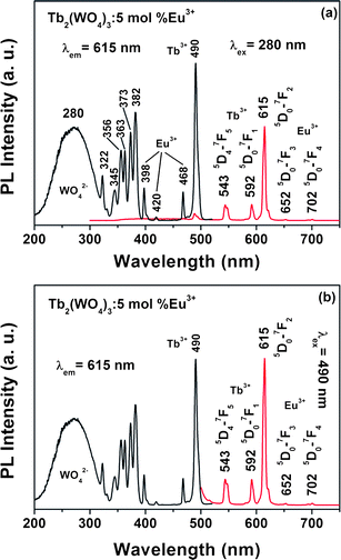 | ||
| Fig. 4 Excitation and emission spectra of the Tb2(WO4)3:5 mol % Eu3+ upon excitation into WO42− (a) and Tb3+ (b). | ||
The kinetic decay curves for the representative emission of Tb3+ (543 nm, 5D4–7F5) in Tb2(WO4)3 and Eu3+ (615 nm, 5D0–7F2) in Tb2(WO4)3:5 mol % Eu3+ were measured, as shown in Fig. 5, respectively. All the decay curves can be well fitted into single-exponential function as I = I0exp(−t/τ), and the lifetime τ values can be determined. The fluorescence lifetimes for Tb3+ (measured at 543 nm) is 0.22 ms in Tb2(WO4)3 nanowires [Fig. 5(a)]. The fluorescence lifetimes for Eu3+5D0 state (measured for 5D0–7F2 at 615 nm) is 0.73 ms in Tb2(WO4)3:5 mol % Eu3+ nanowires.
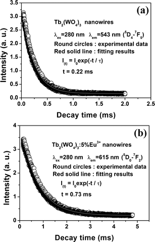 | ||
| Fig. 5 The decay curves for the luminescence of Tb3+ in the Tb2(WO4)3 and Eu3+ in the Tb2(WO4)3:5 mol % Eu3+. | ||
Fig. 6 shows the emission spectra of Tb2(WO4)3:x mol % Eu3+ (x = 0–5) under 490 nm excitation (7F6–5D4 transition of Tb3+). In the undoped Tb2(WO4)3 (x = 0), only the characteristic emissions of Tb3+ are observed. With the doping of Eu3+ (x = 0.3), besides Tb3+ emissions, we can also observe the characteristic emissions of Eu3+. With the increase of Eu3+ concentration, the luminescence of Tb3+ begins to decrease, and that of Eu3+ increases firstly, both due to the enhancing the probability of energy transfer from Tb3+ to Eu3+ along with the increase of Eu3+ concentration. The luminescence of Eu3+ reaches the maximum at x = 5, and then begins to decrease due to the concentration quenching effect (figures not shown due to the limited space). The above results indicate an efficient energy transfer from Tb3+ to Eu3+. Also, such energy transfer behavior shows that the as-synthesized Tb2(WO4)3:Eu3+ is not a mixture of Tb2(WO4)3 and Eu2(WO4)3, but a solid solution, in which Eu3+ has successfully incorporated into Tb2(WO4)3 lattice. Otherwise, the Tb3+ → Eu3+ energy transfer can not occur in the separated phases. The PL color can be tuned from green, brown, orange to red by changing the doping concentration of Eu3+ ions due to different energy transfer efficiencies at different Eu3+concentration. Fig. 7 shows luminescence photographs of Tb2(WO4)3:x mol % Eu3+ nanowires ethanol solutions (0.5 mM) upon excitation with 254 nm from a UV lamp, in which tuning of the emission color from green to red can be realized.
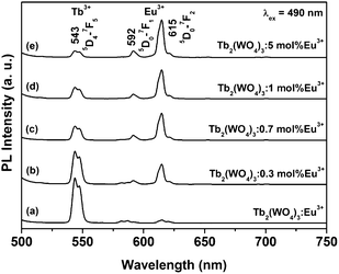 | ||
| Fig. 6 Emission spectra of the Tb2(WO4)3:x mol % Eu3+ samples with different concentration (x = 0–5) under 490 nm excitation. | ||
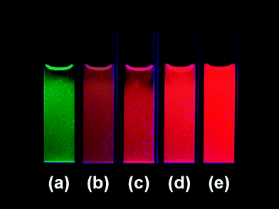 | ||
| Fig. 7 Luminescence photographs of Tb2(WO4)3:x mol % Eu3+ nanowires dispersed in the ethanol solutions, (a) x = 0, (b) x = 0.3, (c) x = 0.7, (d) x = 3, (e) x = 5. | ||
In order to study the energy transfer process in Tb2(WO4)3:Eu3+ in more detail, time-resolved emission spectra of Tb2(WO4)3:5 mol % Eu3+ were measured by excitation into the WO42− band with a 285 nm laser. The emission spectra collected at different delay times (td) are shown in Fig. 8. When td = 10 ns, the spectrum exhibits two types of emission, namely, the characteristic line emission from Tb3+ and Eu3+. Tb3+ and Eu3+ emission are present because the excitation energy of WO42− has been transferred to Tb3+ and Eu3+ within this short time, respectively. When td = 500 ns, the emission of Tb3+ starts to decrease accompanied by the increasing of Eu3+ emissions intensity due to the energy transfer from Tb3+ to Eu3+. The emission of Tb3+ decreases gradually with further increase of the delay time, while that of Eu3+ increases due to transfer of more excitation energy from Tb3+ to Eu3+. When td = 50 μs, the emission intensity of Tb3+ is very weak, and the emission spectrum contains mainly that of Eu3+. When td > 50 μs, the Eu3+ emission also begins to decay gradually and disappears finally due to the depopulation of the excited states (figures not shown due to the limited space).
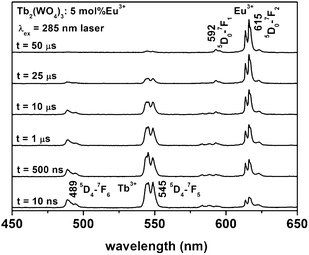 | ||
| Fig. 8 Time-resolved PL spectra of the Tb2(WO4)3:5 mol % Eu3+ sample (λex = 285 nm laser). | ||
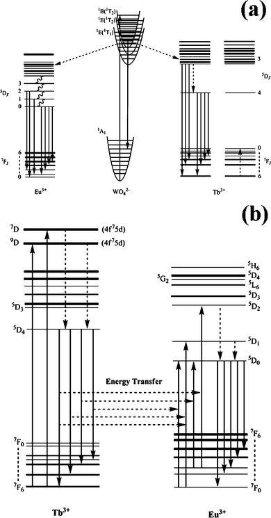
A summary of the emission and energy transfer process in Tb2(WO4)3:Eu3+ is shown schematically in Fig. 9. The emission process for WO42− and the energy transfer from WO42− to Tb3+ and Eu3+ are shown in Fig. 9(a). Upon UV (280 nm) excitation, an electron in the ground state (1A1) is excited into the 1B (1T2) level of WO42−, where the electron either relaxes to its lowest excited 1B (1T2) level of WO42−, producing the emission by the transition to the 1A1 level, or the excitation energy transfers to Eu3+5D3 or higher levels by resonance process, from which the energy nonradiatively relaxes to the 5D0 level by multiphonon relaxation. Then the characteristic emission of 5D0–7FJ (J = 0, 1, 2, 3, 4) occurs. The excitation energy of WO42− mainly transfers to 5D3 or higher levels of Tb3+. The relaxation from 5D3 to 5D4 cannot happen by a multiphonon relaxation process due to the large energy difference between these two levels.16 In view of the high concentration (5 mol %), the relaxation from 5D3 to 5D4 of Tb3+ mainly occurred by the cross-relaxation process. For Tb3+, the energy difference between 5D3 and 5D4 is equal to that between 7F0 and 7F6. The emission process for Tb3+ and the energy transfer between Tb3+ and Eu3+ are shown in Fig. 9(b).8 Firstly, electrons on Tb3+ ions are excited from the ground state (4f8) to the excited state (4f75d) by UV light. Subsequently, these electrons relax to the lowest excited state 5D4 through multiphonon relaxation then either return to the ground state to produce the Tb3+ emissions (5D4–7F6, 5, 4, 3), or transfer their excitation energy from 5D4 (Tb3+) level to the higher excited energy levels of Eu3+ (4f6) through cross relaxation, which relax to the 5D0 (Eu3+) level, where the red-orange emission (5D0–7F0, 1, 2, 3, 4, 5, 6) takes place. Since the 5D4–7F6, 5, 4, 3 emission of Tb3+ is effectively overlapped with the 7F0, 1–5D0, 1, 2 absorption of Eu3+, the energy transfer from Tb3+ to Eu3+ is very efficient.17
 | ||
| Fig. 9 Schematic diagram for the energy transfer from WO42− to Tb3+ and Eu3+ as well as the emission process from Ln3+ (a), and the energy transfer from Tb3+ to Eu3+ (b). | ||
Cathodoluminescence properties
Similar to the emission under UV excitation, the Tb2(WO4)3 and Tb2(WO4)3:5 mol % Eu3+ samples also exhibit strong green and red light, respectively, upon excitation with an electron beam (Tb2(WO4)3: accelerating voltage = 4 kV, filament current = 103 mA; Tb2(WO4)3:5 mol % Eu3+: accelerating voltage = 4 kV, filament current = 100 mA). Typical emission spectra are shown in Fig. 10(a) and (b), respectively. For the undoped Tb2(WO4)3 and Tb2(WO4)3:5 mol % Eu3+, the CL emission spectrum is basically identical with their PL spectra [Fig. 3(a) and 4(a)].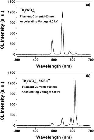 | ||
| Fig. 10 Typical cathodoluminescence spectra of the Tb2(WO4)3 (a) and Tb2(WO4)3:5 mol % Eu3+ (b). | ||
The CL intensity for the Tb2(WO4)3 and Tb2(WO4)3:5 mol % Eu3+ samples were investigated as a function of the accelerating voltage and the filament current, as shown in Fig. 11, respectively. The filament current of Tb2(WO4)3 [Fig. 11(a)] is fixed at 103 mA and that of Tb2(WO4)3:5 mol % Eu3+ [Fig. 11(b)] is fixed at 100 mA, the CL intensity increases with the accelerating voltage from 3 to 5 kV, respectively. Similarly, when the accelerating voltage is fixed at 4 kV, the CL intensity also increases with raising the filament current from 93 to 106 mA of Tb2(WO4)3 [Fig. 11(c)] and from 90 to 104 mA of Tb2(WO4)3:5 mol % Eu3+ [Fig. 11(d)]. The increase in CL brightness with an increasing electron energy and filament current can be attributed to deeper penetration of electrons into the phosphors and the larger electron beam current density. The electron penetration depth can be estimated using the empirical formula L/Å = 250(A/ρ)(E/Z1/2)n, where n = 1.2/(1 − 0.29log10Z), A is the atomic or molecular weight of the material, ρ is the bulk density, Z is the atomic number or the number of electrons per molecule in the case compounds, and E is the accelerating voltage (kV).18 For cathodoluminescence, the Ln3+ ions are excited by the plasma produced by the incident electrons. The deeper the electron penetration depth, the more the plasma will be produced, which resulted in more Ln3+ ions being excited and thus the CL intensity increased.
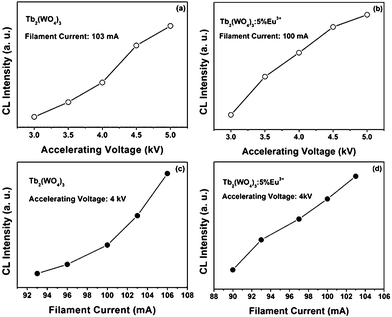 | ||
| Fig. 11 The cathodoluminescence intensity of Tb2(WO4)3 and Tb2(WO4)3:5 mol % Eu3+ nanowires as a function of accelerating voltage (a, b) and filament current (c, d). | ||
4. Conclusions
In summary, one-dimensional Tb2(WO4)3 and Tb2(WO4)3:Eu3+ nanomaterials have been successfully synthesized by means of electrospinning technique in conjunction with sol–gel process. The as-form hybrid precursor materials present uniform fiberlike morphology. After annealing the precursors at high temperature, the as-prepared samples with wire morphology are well crystallized with the monoclinic structure of Tb2(WO4)3. Due to an efficient energy transfer from the WO42−group to Tb3+ ions, Tb3+ ions show its characteristic strong emissions in the 1D Tb2(WO4)3 nanowires upon excitation into the WO42−group at 280 nm and Tb3+ at 490 nm. Due to an efficient energy transfer from the WO42−group to Tb3+/Eu3+ ions and from Tb3+ ions to Eu3+ ions, Eu3+ ions show its characteristic strong emissions in the Tb2(WO4)3:5 mol % Eu3+ 1D nanowires upon excitation into the WO42−group at 280 nm and Tb3+ at 490 nm. Under low-voltage electron beam excitation, Tb2(WO4)3 and Tb2(WO4)3:5 mol % Eu3+ phosphors show green emission of Tb3+ and red emission of Eu3+, respectively. These studies indicate that electrospinning is a facile and novel route for the development 1D luminescent nanomaterials that are useful in many types of lighting and color display fields.Acknowledgements
This project is financially supported by National Basic Research Program of China (Grant Nos. 2007CB935502, 2010CB327704), and the National Natural Science Foundation of China (Grant Nos. NSFC 50702057, 50872131, 20921002).References
- (a) Q. Tang, Z. P. Liu, S. Li, S. Y. Zhang, X. M. Liu and Y. T. Qian, J. Cryst. Growth, 2003, 259, 208 CrossRef CAS; (b) J. A. Capobianco, F. Vetrone, J. C. Boyer, A. Speghini and M. Bettinelli, Opt. Mater., 2002, 19, 259 CrossRef CAS; (c) M. S. Palmer, M. Neurock and M. M. Olken, J. Am. Chem. Soc., 2002, 124, 8452 CrossRef CAS; (d) Y. Hasegawa, S. Thongchant, Y. Wada, H. Tanaka, T. Kawai, T. Sakata, H. Mori and S. Yanagida, Angew. Chem., 2002, 114, 2177 CrossRef; (e) A. X. Yin, Y. W. Zhang, L. D. Sun and C. H. Yan, Nanoscale, 2010, 2, 953 RSC.
- (a) P. D. Rack, A. Naman, P. H. Holloway, S. S. Sun and R. T. Tuenge, Mater. Res. Bull., 1996, 21, 49 CAS; (b) X. Piao, T. Horikawa, H. Hanzawa and K. Machidaa, Appl. Phys. Lett., 2006, 88, 161908 CrossRef; (c) J. K. Park, K. J. Choi, J. H. Yeon, S. J. Lee and C. H. Kim, Appl. Phys. Lett., 2006, 88, 043511 CrossRef; (d) M. G. Ko, J. C. Park, D. K. Kim and S. H. Byeon, J. Lumin., 2003, 104, 215 CrossRef CAS; (e) L. Zhou, W. C. H. Choy, J. Shi, M. Gong, H. Liang and T. I. Yuk, J. Solid State Chem., 2005, 178, 3004 CrossRef CAS; (f) B. L. Abrams and P. H. Holloway, Chem. Rev., 2004, 104, 5783 CrossRef CAS; (g) H. L. Li, Z. L. Wang, S. J. Xu and J. H. Hao, J. Electrochem. Soc., 2009, 156, J112 CrossRef CAS; (h) K. S. Sohn, D. H. Park, S. H. Cho, J. S. Kwak and J. S. Kim, Chem. Mater., 2006, 18, 1768 CrossRef CAS.
- (a) A. V. Murugan, A. K. Viswanath, V. Ravi, B. A. Kakade and V. Saaminathan, Appl. Phys. Lett., 2006, 89, 123120 CrossRef; (b) G. Wakefield, E. Holland, P. J. Dobson and J. L. Hutchison, Adv. Mater., 2001, 13, 1557 CrossRef CAS; (c) F. Zhang, S. Yang, C. Stooffers, J. Penczek, P. N. Yocom, D. Zaremba, B. K. Wangner and C. J. Summers, Appl. Phys. Lett., 1998, 72, 2226 CrossRef CAS; (d) Y. Shimomura and N. Kijima, J. Electrochem. Soc., 2004, 151, H86–H92 CrossRef CAS; (e) S. S. Yi, J. S. Bae, B. K. Moon, J. H. Jeong and J. H. Kim, Appl. Phys. Lett., 2005, 86, 071921 CrossRef; (f) J. Y. Cho, Y. R. Do and Y. D. Huh, Appl. Phys. Lett., 2006, 89, 131915 CrossRef; (g) H. S. Jang, J. H. Kang, Y. H. Won, S. Lee and D. Y. Jeon, Appl. Phys. Lett., 2007, 90, 071908 CrossRef; (h) X. Y. Chen, E. Ma and G. K. Liu, J. Phys. Chem. C, 2007, 111, 10404 CrossRef CAS.
- (a) G. Blasse, B. C. Grabmaier, Luminescent Materials, Springer-Verlag: Berlin Heideberg, 1994 Search PubMed; (b) R. C. Evans, L. D. Carlos, Peter. Douglas and J. Rocha, J. Mater. Chem., 2008, 18, 1100 RSC; (c) P. Ghosh, A. Kar and A. Patra, Nanoscale, 2010, 2, 1196 RSC.
- (a) E. Nakazawa and S. Shionoya, J. Chem. Phys., 1967, 47, 3211 CAS; (b) Z. L. Wang, J. H. Hao and H. L. W. Chan, J. Electrochem. Soc., 2010, 157, J315 CrossRef CAS.
- L. P. Johnson, J. E. Geusic and Van L. C. Uitert, Appl. Phys. Lett., 1966, 8, 200 CrossRef CAS.
- (a) Y. S. Liu, W. Q. Luo, R. F. Li, G. K. Liu, M. R. Antonio and X. Y. Chen, J. Phys. Chem. C, 2008, 112, 686 CrossRef CAS; (b) A. Kar, A. Datta and A. Patra, J. Mater. Chem., 2010, 20, 916 RSC; (c) K. S. Sohn, N. Shin, Y. C. Kim and Y. R. Do, Appl. Phys. Lett., 2004, 85, 55 CrossRef CAS.
- (a) W. W. Holloway, M. Kestigian and R. Newman, Phys. Rev. Lett., 1963, 11, 458 CrossRef CAS; (b) W. Chen, R. Sammynaiken and Y. Huang, J. Appl. Phys., 2000, 88, 1424 CrossRef CAS; (c) T. Kim Anh, T. Ngoc, P. Thu Nga, V. T. Bitch, P. Long and W. Strek, J. Lumin., 1988, 39, 215 CrossRef; (d) A. Moadhen, H. Elhouichet, B. Canut, C. S. Sandu, M. Oueslati and J. A. Roger, Mater. Sci. Eng., B, 2003, 105, 157 CrossRef; (e) Z. J. Zhang, H. H. Chen, X. X. Yang and J. T. Zhao, Mater. Sci. Eng., B, 2007, 145, 34 CrossRef CAS; (f) W. H. Di, X. J. Wang, P. F. Zhu and B. J. Chen, J. Solid State Chem., 2007, 180, 467 CrossRef CAS; (g) T. Kim Anh and W. Strek, J. Lumin., 1988, 42, 205 CrossRef.
- (a) S. Madhugiri, A. Dalton, J. Gutierrez, J. P. Ferraris and K. J. Balkus Jr, J. Am. Chem. Soc., 2003, 125, 14531 CrossRef CAS; (b) L. Yao, T. W. Haas, A. Guiseppi-Elie, G. L. Bowlin, D. G. Simpson and G. E. Wnek, Chem. Mater., 2003, 15, 1860 CrossRef CAS; (c) G. Larsen, R. Velarde-Ortiz, K. Minchow, A. Barrero and I. G. Loscertales, J. Am. Chem. Soc., 2003, 125, 1154 CrossRef CAS; (d) H. Q. Hou and D. H. Reneker, Adv. Mater., 2004, 16, 69 CrossRef CAS; (e) J. J. Ge, H. Hou, Q. Li, M. J. Graham, A. Greiner, D. H. Reneker, F. W. Harris and S. Z. D. Cheng, J. Am. Chem. Soc., 2004, 126, 15754 CAS; (f) M. J. Li, J. H. Zhang, H. Zhang, Y. F. Liu, C. L. Wang, X. Xu, Y. Tang and B. Yang, Adv. Funct. Mater., 2007, 17, 3650 CrossRef.
- P. Yang, M. K. Lu, C. F. Song, G. J. Zhou, D. Xu and D. R. Yuan, J. Phys. Chem. Solids, 2002, 63, 2047 CAS.
- X. A. Fu and S. Qutubuddin, Colloids Surf., A, 2001, 186, 245 CrossRef.
- J. W. Zhai, L. Y. Zhang, X. Yao and S. N. B. Hodgson, Surf. Coat. Technol., 2001, 138, 135 CrossRef.
- (a) M. M. Bergshoef and G. J. Vancso, Adv. Mater., 1999, 11, 1362 CrossRef CAS; (b) X. Y. Wang, C. Drew, S. H. Lee, K. J. Senecal, J. Kumar and L. A. Samuelson, Nano Lett., 2002, 2, 1273 CrossRef CAS; (c) C. L. Casper, J. S. Stephens, N. G. Tassi, D. B. Chase and J. F. Rabolt, Macromolecules, 2004, 37, 573 CrossRef CAS; (d) D. A. Czaplewski, S. S. Verbridge, J. Kameoka and H. G. Craighead, Nano Lett., 2004, 4, 437 CrossRef CAS.
- (a) B. Chamberland, J. Kafalas and J. Goodenough, Inorg. Chem., 1977, 16, 44 CrossRef CAS; (b) T. Takagi and J. Fukazawa, Appl. Phys. Lett., 1980, 36, 278 CrossRef; (c) L. Uitert and S. Preziosi, J. Appl. Phys., 1962, 33, 2908 CrossRef; (d) H. Wang, F. Medina, Y. Zhou and Q. Zhang, Phys. Rev. B: Condens. Matter, 1992, 45, 10356 CrossRef CAS; (e) K. Tanaka, T. Miyajima, N. Shirai, Q. Zhang and R. Nakata, J. Appl. Phys., 1995, 77, 6581 CrossRef CAS; (f) V. B. Mikhailik, H. Kraus, D. Wahl, M. Itoh, M. K. Koike and I. K. Bailiff, Phys. Rev. B: Condens. Matter Mater. Phys., 2004, 69, 205110 CrossRef; (g) V. B. Mikhailik, I. K. Bailiff, H. Kraus, P. A. Rodnyi and J. Ninkovic, Radiat. Meas., 2004, 38, 585 CrossRef CAS.
- (a) B. Grobelna, Optica Applicata, 2008, XXXVIII, 39 Search PubMed; (b) B. Grobelna, J. Alloys Compd., 2007, 440, 265 CrossRef CAS; (c) H. Naruka and D. M. Obaid, J. Lumin., 2009, 129, 1132 CrossRef.
- G. Blasse and A. Bril, Philips Res. Rep., 1967, 22, 481 Search PubMed.
- E. Nakazawa and S. Shionoya, J. Chem. Phys., 1967, 47, 3211 CAS.
- (a) J. X. Wan, Z. H. Wang, X. Y. Chen, L. Mu and Y. T. Qian, J. Cryst. Growth, 2005, 284, 538 CrossRef CAS; (b) J. Yang, X. M. Liu, C. X. Li, Z. W. Quan, D. Y. Kong and J. Lin, J. Cryst. Growth, 2007, 303, 480 CrossRef CAS; (c) J. Yang, C. X. Li, Z. Y. Cheng, X. M. Zhang, Z. W. Quan, C. M. Zhang and J. Lin, J. Phys. Chem. C, 2007, 111, 18148 CrossRef CAS.
| This journal is © The Royal Society of Chemistry 2011 |