Preparation of ideal molecular junctions: depositing non-invasive gold contacts on molecularly modified silicon
Richard T. W.
Popoff
a,
Karen L.
Kavanagh
*b and
Hua-Zhong
Yu
*a
aDepartment of Chemistry, Simon Fraser University, Burnaby, British Columbia V5A 1S6, Canada. E-mail: hogan_yu@sfu.ca
bDepartment of Physics, Simon Fraser University, Burnaby, British Columbia V5A 1S6, Canada. E-mail: kavanagh@sfu.ca
First published on 3rd February 2011
Abstract
Recent advances in creating rectifying gold|monolayer|silicon (Au–M–Si) junctions (namely, molecular silicon diodes) are reviewed. It is known that direct deposition of gold contacts onto molecular monolayers covalently bonded to silicon surfaces causes notable disruption to the junction structure, resulting in deteriorated performance and poor reproducibility that are unsuitable for practical applications. In the past few years, several new experimental approaches have been explored to minimize or eliminate such damage, including the “indirect” evaporation method and the pre-deposition of a protective “non-penetrating” metal. To enhance the interactions at the gold–monolayer interface, head-groups that allow bonding to gold are used to maintain the monolayer integrity. Construction of the device via flip-chip lamination and the modified polymer-assisted lift-off techniques also prohibits monolayer damage. Refining the fabrication and design techniques towards reliable molecular junctions is crucial if they are to be used in nanoelectronics for the purpose of miniaturization.
 Richard T. W. Popoff | Richard Popoff received his BSc in Chemistry from Simon Fraser University (SFU), Canada, in May 2007. He worked as an undergraduate research assistant in Prof. Erika Plettner's group on organic synthesis of natural products and then joined Dr Hogan Yu's laboratory at 4D Labs as a PhD candidate in September 2007. His research interests include molecular modification of semiconductor materials, fabrication of metal–molecule–semiconductor junctions, and investigation of charge transport mechanisms across molecular interfaces. |
 Karen L. Kavanagh | Karen Kavanagh received her BSc in Chemical Physics from Queen's University (Canada) and her PhD in Materials Science and Engineering from Cornell University. She was a Postdoctoral Fellow at Massachusetts Institute of Technology and then at IBM's T. J. Watson Research Center. She moved through the ranks from Assistant to full Professor in Electrical and Computer Engineering at the University of California, San Diego before moving to SFU where she is a Professor of Physics. Her research is focused on structure–property correlations in electronic materials. She has extensive expertise in a range of materials characterization techniques including: scanning transmission electron microscopy (STEM), high resolution X-ray diffraction, Rutherford backscattering spectroscopy (RBS), scanning tunnelling microscopy (STM) and ballistic electron emission microscopy (BEEM). |
 Hua-Zhong Yu | Hua-Zhong (Hogan) Yu received his PhD from Peking (Beijing) University (with Zhong-Fan Liu) in 1997. He was a postdoctoral fellow first at California Institute of Technology working with Ahmed Zewail (1999 Nobel Laureate in Chemistry) and Fred Anson, and then at NRC's Steacie Institute of Molecular Sciences with Dan Wayner. In 2001, he joined SFU as an Assistant Professor in Chemistry, and was granted early promotions to Associate Professor (2005) and Professor (2009). He also holds joint appointments with 4D Labs (Center for Advanced Materials and Nanostructures) and the Department of Molecular Biology and Biochemistry. Dr Yu's research spans a broad range of analytical chemistry and materials science; he is particularly interested in surface modification with self-assembled monolayers, fabrication of nanostructured materials, and the development of biosensing devices. |
1. Introduction
Nanotechnology is currently one of the most active areas of research since many electronic or photonic devices are approaching limits to their manufacturing via traditional materials and methods.1–3 New fabrication methods or new electronic materials are required in order to construct new devices.4 Chemical modification of semiconductor–metal interfaces by an organic monolayer to construct a molecularly tuneable metal|monolayer|semiconductor (MMS) junction is one of many plausible avenues. Changing the monolayer chemical compositions can modulate the electrical characteristics of an MMS junction, and has been extensively investigated over the past decade.5–23Knowledge about the electronic properties of MMS junctions has been gained by using “soft” metal contacts (e.g., mercury drop).5–11,24 A schematic illustration of a mercury (Hg) drop used to form a junction on freshly etched silicon (H–Si![[triple bond, length as m-dash]](https://www.rsc.org/images/entities/char_e002.gif) ), and organically modified silicon (MSi) is shown in Fig. 1.10 In this approach, a controlled volume of Hg is pumped from a clean reservoir onto the sample surface to be contacted. The resulting current versus voltage characteristics of a Hg|H–Si junction are linear at room temperature indicating an ohmic contact, modeled as a resistor in Fig. 1(a).10 With the addition of an organic monolayer, such junctions develop a larger electrical barrier and become rectifying (Fig. 1(b)).10 An optical image of the mercury drop making contact with a silicon (Si) surface is shown in Fig. 1(c).10 While Hg contacts are acceptable for research purposes, it is unlikely to be included in the construction of a practical device. Its high surface tension and low reactivity lead to it to “float” on the monolayer interface, i.e., the contacts will not stay in fixed positions. Under ambient conditions, H–Si surfaces are prone to oxidation25,26 and contamination,26 and the associated health concerns of Hg make it unsuitable for commercial use.
), and organically modified silicon (MSi) is shown in Fig. 1.10 In this approach, a controlled volume of Hg is pumped from a clean reservoir onto the sample surface to be contacted. The resulting current versus voltage characteristics of a Hg|H–Si junction are linear at room temperature indicating an ohmic contact, modeled as a resistor in Fig. 1(a).10 With the addition of an organic monolayer, such junctions develop a larger electrical barrier and become rectifying (Fig. 1(b)).10 An optical image of the mercury drop making contact with a silicon (Si) surface is shown in Fig. 1(c).10 While Hg contacts are acceptable for research purposes, it is unlikely to be included in the construction of a practical device. Its high surface tension and low reactivity lead to it to “float” on the monolayer interface, i.e., the contacts will not stay in fixed positions. Under ambient conditions, H–Si surfaces are prone to oxidation25,26 and contamination,26 and the associated health concerns of Hg make it unsuitable for commercial use.
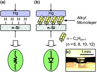 | ||
| Fig. 1 Schematic illustration of mercury|silicon junctions and their electrical characteristics. (a) A direct Hg|H–Si (n-type) junction exhibits ohmic contact characteristics at room temperature due to a lower Schottky barrier (0.43 eV), represented as a resistor. (b) An alkyl monolayer junction, Hg|CnH2n+1–Si (n = 6, 8, 10, 12), shows rectifying behavior, represented as a diode. (c) An optical photograph shows the mercury drop (and its mirror image) in contact with the silicon surface. Y. J. Liu and H. Z. Yu, Alkyl monolayer-passivated metal-semiconductor diodes: molecular tunability and electron transport, ChemPhysChem, 2002, 3, 799–802. Copyright Wiley-VCH Verlag GmbH & Co. KGaA. Reproduced with permission. | ||
Gold (Au) is probably the most favourable metal for device purposes. It is chemically inert under ambient conditions and has a high electrical conductivity. Two of the most researched semiconductors for MMS junctions are Si and gallium–arsenide (GaAs). The molecular contacts to Si, and the fabrication and experimental characteristics of these contacts, will be the primary focus of this review. Theoretical investigations of their electronic characteristics have been covered in literature reports and will not be further discussed here.27,28
One basic challenge for the fabrication of a reliable Au contact to an organically modified Si surface is to prevent the formation of Au–Si alloys at the interface. The Au–Si equilibrium, binary phase diagram (inert atmosphere) shows a single eutectic at ∼17% of Si, ∼370 °C.29 Thus, at room temperature, single phase Si (saturated in Au) and Au (saturated in Si) are in thermodynamic equilibrium. When forming an intimate Au–Si contact under ambient conditions, interdiffusion would proceed until both sides reach equilibrium solubility. Room temperature interdiffusion in vacuum is detected by X-ray reflectivity measurements30 at rates that depend on the interface preparation. This interdiffusion is also associated with lower Au–Si Schottky barrier characteristics (ohmic characteristics at room temperature) for diodes prepared and maintained under ultra-high-vacuum (UHV) conditions.31 In UHV the formation of Au3Si surface alloy is observed when Au is deposited onto reconstructed Si(111) surfaces.32 A further challenge with Au is that it also can form alternative conduction pathways through an organic film creating a low-resistance abnormality, or ‘short’, within the device.33,34
The presence of ambient oxygen or water vapour changes the equilibrium condition to include surface oxidation of the Si after it has diffused through the Au. This process accelerates at higher annealing temperatures, and SiO2 layers form in proportion to the thickness of the Au.35 The diffusion of oxygen to the interface is observed to be correlated with an increase in the Au–Si barrier height as a function of time exposed to air or water.36
When an organic monolayer passivates Si surface, it is likely that Au will diffuse to the Si first through pinholes or defects in the monolayer, regardless of the deposition method. This diffusion will be inhibited if the Au layer is bonded to the monolayer or if the surface energy of the Au/monolayer interface is low, or in other words, Au “wets” the monolayer surface.
Many techniques for placing a metal contact onto a molecularly modified silicon wafer have been tested.33,34 The chemical composition of the monolayer itself may also play a role in the durability of Au–M–Si junctions.13,14 In the following sections, we will describe recent progress towards understanding the structural disruption of the monolayer upon direct Au deposition, and in developing novel experimental approaches for the construction of ideal molecular junctions.
2. Construction of molecular diodes from organically modified silicon
The integrity of the monolayer after Au has been deposited onto a modified Si wafer, and the chemical modifications carried out on the Si surface, must be well understood if these types of junctions are ever to be used practically. The molecular composition and orientation of the monolayer may hold the key to limiting Au from penetrating through the organic film. By examining more closely the monolayer–silicon interface, Au–monolayer interface, and the monolayer itself, a better understanding of Au penetration can be gained. There is a clear correlation between the monolayer composition and the degree of metal penetration that occurs when constructing Au–M–Si junctions.12–16,372.1 Formation of molecular monolayers on silicon
The silicon wafers that have been used for the construction of Au–M–Si junctions are either Si(100) or Si(111) with various dopant type, dopant density, and electrical conductivity. The two surface orientations have different structural properties: most significantly the density of Si–Si bonds is lower for (100) compared to (111) (Fig. 2).38 Each requires different etchants to produce the flattest surface after removal of the native oxide, using hydrofluoric acid (HF) and ammonium fluoride (NH4F), respectively.38 These etchants attack silicon–oxygen bonds leaving a dihydride or monohydride bonded Si surface, respectively. However, for covalent bonding to n-alkyl (R) monolayers, the surface chemistry of Si(100) or Si(111) is similar since both surfaces involve the reaction of H–Si bonds.38,39 One of the more frequently used methods reported in the literature is reacting an alkene,14–16,40–46 or alkyne,15,40 with H–Si. The H–Si bond can be activated and can react via heating or exposure to ultraviolet radiation which generates a radical at the silicon surface (Si˙). This can form a Si–C bond when exposed to, for example, a terminal alkene (CH2![[double bond, length as m-dash]](https://www.rsc.org/images/entities/char_e001.gif) CH–R), resulting in a radical on the second carbon (Si–CH2˙–CH–R). This reaction occurs most likely by abstracting hydrogen from a neighbouring H–Si bond and a new Si surface radical is formed.39 Monolayers on H–Si have also been reported by using either alkoxies or alcohols (−O–R)12,16,47 or Grignard reagents (RMgX, where Mg = magnesium and X is a halide)9,10,13 that follow different reaction mechanism.39 These reactions are different from the condensation of alkylsilanes (R–SiL3, where L is a leaving group such as chlorine or methoxide) and their derivatives, on oxidized silicon. In other words, alkylsilanes react directly with the oxide of silicon instead of H–Si surfaces.12,37
CH–R), resulting in a radical on the second carbon (Si–CH2˙–CH–R). This reaction occurs most likely by abstracting hydrogen from a neighbouring H–Si bond and a new Si surface radical is formed.39 Monolayers on H–Si have also been reported by using either alkoxies or alcohols (−O–R)12,16,47 or Grignard reagents (RMgX, where Mg = magnesium and X is a halide)9,10,13 that follow different reaction mechanism.39 These reactions are different from the condensation of alkylsilanes (R–SiL3, where L is a leaving group such as chlorine or methoxide) and their derivatives, on oxidized silicon. In other words, alkylsilanes react directly with the oxide of silicon instead of H–Si surfaces.12,37
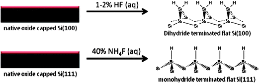 | ||
| Fig. 2 Fluoride-based etching conditions, leading to hydride-terminated flat silicon surfaces. Adapted with permission from ref. 38. Copyright 2002, American Chemical Society. | ||
2.2 Monolayer composition at the monolayer–silicon interface
Characterization of monolayers prepared through each of the above reaction methods finds them to be of different qualities. Their properties are dependent primarily on the monolayer linker (e.g. Si–C versus Si–O–C),8,25 the monolayer composition43,48 and the organic chain length,9,10 not only the method of synthesis.39,44,49,50 Being the shortest alkyl monolayer, methyl (CH3−) termination is the simplest, reacting in a 1![[thin space (1/6-em)]](https://www.rsc.org/images/entities/char_2009.gif) :1 ratio with H–Si to form carbon–silicon bonds, CH3–Si.51–53X-Ray photoelectron spectroscopy (XPS) reveals that longer organic molecules react with fewer H–Si sites under the same conditions.52 The theoretical maximum ratio of reacting H–Si for alkyl monolayers is calculated to be 0.69:1.54 For example, 1-octene is reported to react at approximately a 0.6:1 ratio with available H–Si.52 This is likely caused by an increase in steric strain at the silicon surface, as the distance between silicon atoms is not adequate to accommodate the bonded organic molecules.52,54
:1 ratio with H–Si to form carbon–silicon bonds, CH3–Si.51–53X-Ray photoelectron spectroscopy (XPS) reveals that longer organic molecules react with fewer H–Si sites under the same conditions.52 The theoretical maximum ratio of reacting H–Si for alkyl monolayers is calculated to be 0.69:1.54 For example, 1-octene is reported to react at approximately a 0.6:1 ratio with available H–Si.52 This is likely caused by an increase in steric strain at the silicon surface, as the distance between silicon atoms is not adequate to accommodate the bonded organic molecules.52,54
There are potentially many defects in the monolayer besides the unreacted H–Si sites on either the planes or terraces of the sample. Contact angle and ellipsometric techniques can provide macroscopic information about the monolayer quality,12,14,16,45 while Fourier-transform infrared (FTIR)12,16,24,55–57 and vibrational sum-frequency generation (SFG)45spectroscopy measurements indicate that the monolayers on silicon are generally well-ordered. Although there may be unreacted H–Si sites across a modified silicon surface, this does not necessarily indicate the monolayers are of poor quality. The above spectroscopic techniques allow us to deduce that the monolayers do not orient themselves perfectly parallel to the surface normal:39,54 the molecules are tilted towards the surface allowing for closer interaction via van der Waals forces resulting in a quasi-crystalline structure.54
Organic monolayers bonded to the surface of silicon oxide are significantly more robust upon gold deposition.12,16 When comparing the reflection and adsorption infrared spectra of Au|monolayer|SiOx–Siversus Au|monolayer|Si junctions, the latter junction has a complete loss of the monolayer signal (diminished methyl and methylene FTIR stretching bands).12,16 This is correlated with slower Au–Si interdiffusion at Au/silicon oxide interfaces based on X-ray scattering measurements.32 Their higher Schottky barriers36,58 suggest that the Au evaporation process is not as important to monolayer destruction as is Au–Si interdiffusion. Penetrating Au atoms will interact with remaining H–Si at a monolayer–silicon interface to form Au–Si alloy, whereas the oxidized Si interlayer inhibits this reaction.16,30,32,35,36,58,59 During the Au–Si alloy formation, it is also possible that Si–C and Si–O–C linkages are susceptible to heterolysis, typically observed in organosilane chemistry,12,13,16,18,55,60 by which the monolayers are eventually detached from the Si surface.
Oxide formation26,44,46,61 on modified Si samples also causes changes to the properties of an MMS device. Several reports have shown clearly that oxidation has a significant effect on the electrical performance of modified silicon,26,44,46,61 and even trace amounts of oxide growth can cause noticeable difference.46 Shown in Fig. 3 are current–density versus voltage plots of samples as a function of oxidization times under ambient conditions. Organic monolayers in plots (a) are “C12”, or CH3–(CH2)11–Si, exposed and measured at intervals of 0, 8, 58, 93 and 134 days, while in (b) are “C3Ph”, or C6H5–(CH2)3–Si, exposed and measured at intervals of 0, 10, 86, 121 and 162 days.46 Measurable oxidation occurs after each interval changing the overall properties of these MMS junctions.46
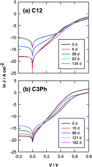 | ||
| Fig. 3 Representative current density vs. bias voltage (J–V) plots for freshly prepared and aged molecular junctions. (a) Hg|CH3–(CH2)11–Si: the CH3–(CH2)11–Si samples were exposed to ambient conditions for 0, 8, 58, 93, and 134 days. (b) Hg|C6H5–(CH2)3–Si: the C6H5–(CH2)3–Si samples for 0, 10, 86, 121, and 162 days. Reprinted with permission from ref. 46. Copyright 2010 American Chemical Society. | ||
2.3 The monolayer density
As mentioned above, less than 69% of the available H–Si sites may react during the formation of a monolayer.54 Considering a simple space filling model using a CH3–(CH2)9–Si monolayer, the density of unoccupied sites is consistent with this result. A “ball and stick” model of CH3–(CH2)9–Si molecular attachment to Si (111) is shown in Fig. 4, illustrating unoccupied H–Si sites.62 As mentioned, these available sites62 are the locations where Au is likely to first penetrate the monolayer to reach the underlying silicon.12,16,45,59 Over the past few years, a few reports presented new methods to increase the monolayer density15,40,51 by reacting a terminal n-alkyne (H–CC–R) with H–Si. The alkene functional groups form monolayers with π-stacking characteristics allowing for a significantly higher packing density in comparison to an n-alkyl monolayer.15,40,51Fig. 5 illustrates little difference in monolayer structure at the monolayer–silicon interface between an n-alkyl monolayer and alkenyl monolayer except lateral stacking is more likely for the alkenyl molecules.40 The packing density of organic monolayers on Si has often been quantified using high-resolution XPS analysis of the C–Si bond in the C 1s region (normalized to the Si 2p peak).40,46,52 In monolayers where π-stacking exists, higher packing densities have been interpreted based on a significant increase in C–Si signal.46 The higher density of covalently attached molecules with fewer defects and reductions in the density of unreacted H–Si sites may help to limit the rate of Au penetration through the monolayer.63,64
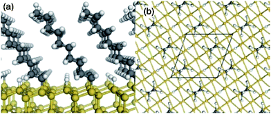 | ||
| Fig. 4 “Ball and stick” models of the slab geometry for simulation of C10H21 alkyl chains bonded to a Si(111) surface. (a) Side view and (b) top view (down the molecular backbone). A single surface unit cell with two alkyl chains and two passivating H atoms is also shown. Reprinted figure with permission from L. Segev, A. Salomon, A. Natan, D. Cahen, and L. Kronik, Phys. Rev. B: Condens. Matter Mater. Phys., 2006, 74, 165323. Copyright 2006 by the American Physical Society. | ||
 | ||
| Fig. 5 Linkages of organic monolayers on H–Si(111): alkyl monolayer (left) and alkenyl monolayer (right). Intermolecular interactions will be different. Reprinted with permission from ref. 40. Copyright 2010 American Chemical Society. | ||
Multilayers can be distinguished from monolayers via various techniques including XPS, FTIR and ballistic electron emission microscopy (BEEM).13,17,36,58,65BEEM studies of Au|pentacene|Si(111) diodes showed that the molecules were either lying flat or standing up.65 These structural differences resulted in different BEEM transmission currents and shifts in the threshold voltage, equivalent to the local interface energy barrier.
2.4 Monolayer composition at the metal–monolayer interface
The functional group on the surface of the monolayer, or monolayer head-group, can influence the extent of Au penetration through the semiconductor-attached monolayer. Most reports have dealt with simple n-alkyl monolayers (with a CH3– head-group at the surface), which are chemically inert with respect to Au.12,13,16,45 A thiol head-group (HS−) can limit Au penetration into the monolayer film via the formation of relatively stable Au–S bonds,13 blocking the subsequently deposited metal from penetrating the monolayer. Cross-sectional transmission electron microscopy (TEM) images, shown in the top section of Fig. 6 at low (left) and high (right) magnification, compare two interfaces.13 The interface in (a) and (b), formed using Au|n-alkyl monolayers|Si(111) with only CH3– head-groups, shows direct interaction between Au and Si with little indication that there is an interfacial monolayer.13 The interface in images (c) and (d) was formed using a thiol-terminated monolayer where a distinct interfacial layer is clearly evident.13 Results from averaged BEEM spectra as a function of monolayer type compared to a reference Au–Si interface are shown in the lower plot of Fig. 6.13 The presence of an organic monolayer reduces the BEEM transmission currents with clear differences between thiol-terminated and CH3-terminated monolayers. Significant lateral variation in the BEEM current across the thiol-terminated monolayer was observed with generally much higher signals for Au|CH3–(CH2)n–Si junctions.13 It is likely that the thiol head-group acts as a “nucleation site” for deposited Au atoms, and prevents or limits Au diffusion through the monolayer to reach the underlying silicon.13 This reduces the BEEM current since tunnelling transmission probabilities are reduced where the insulating monolayer is continuous.
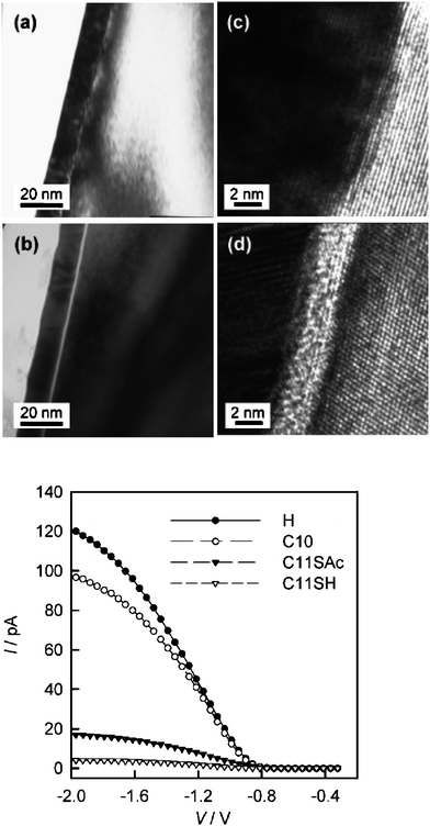 | ||
| Fig. 6 Top: cross-sectional TEM images of the Au|monolayer|Si(111) diode junctions obtained with the beam parallel to the interface along a low-index substrate direction (λ or ξ). (a) Au|C10H21–Si and (b) Au|HS–C11H22––Si: lower magnification bright field (with an objective aperture to enhance contrast). (c and d) Corresponding higher magnification, phase contract images (without an objective aperture). Bottom: averaged BEEM spectra for diode junctions prepared on hydrogen-terminated and organically modified silicon with evaporated gold pads as top contacts. Reprinted with permission from ref. 13. Copyright 2008 American Chemical Society. | ||
3. Conventional methods to prepare Au contacts on molecularly modified silicon
Several challenges have been identified with the direct deposition methods that likely lead to degradation of the organic monolayers. The most commonly used is thermal evaporation under reduced pressure.12,13,16,37,45,55 Most reports indicate that this method yields poor reproducibility of both structural properties and electrical performance.12,13,16,45,55Sputtering deposition has a notably worse effect on the monolayer integrity compared to thermal evaporation.45 Therefore, “indirect” deposition has been explored in more recent studies.14,21,22,33,34,55 Studies which involve other promising techniques to construct MMS junctions will be briefly discussed.24,33,34,56,57,66,673.1 Direct deposition
Direct deposition techniques involve exposing a sample directly to a source of energetic metallic vapour particles that strike the substrate and build up a thin film. Fig. 7 shows an illustration of a direct evaporation chamber where the samples are oriented to directly face the metal source, with optional substrate cooling.34Thermal evaporation, electron-beam deposition, and sputtering are the most common deposition methods used to prepare a thin Au film onto modified Si.12–16,33,37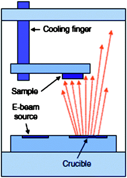 | ||
| Fig. 7 View of vacuum chamber used in direct evaporation. The samples face the metal crucible and evaporation itself occurs at the best vacuum pressure, without the presence of inert gas. Substrate cooling is feasible. Reprinted from H. Haick and D. Cahen, Making contact: connecting molecules electrically to the macroscopic world, Prog. Surf. Sci., 2008, 83, 217–261. Copyright 2008, with permission from Elsevier. | ||
Based on SFG measurements, direct deposition methods (sputtering or thermal evaporation) of thin Au films result in different levels of structural disruption to the monolayer.33 The results are somewhat different from the total displacement of the organic monolayers reported previously, in which heterolytic cleavage of C–Si and O–S bonds was proposed.12,16Sputtering, the more energetic of the two deposition techniques, allows gold atoms to penetrate the monolayer more readily than does thermal evaporation.33 A cartoon illustration of the two situations reproduced from ref. 45 is shown in Fig. 8. A greater degree of penetration to the interface for the sputtered deposition explains their poorer electrical properties observed. In both cases, sufficient damage and disordering are done to the monolayer but the sputter-deposited junction loses its rectification properties.33 Electrical measurements reveal that n-alkyl monolayers with longer chain lengths limit the penetration of Au towards the underlying Si substrate for sputtered samples.33 This is likely because additional methylene groups (−CH2–), present in “thicker” n-alkyl monolayers, prevents the gold atoms from moving completely through the monolayer.68 Thermally deposited Au contact onto modified Si retains the rectification characteristics since presumably less monolayer disruption and decomposition occur.33 Overall, the direct deposition of Au onto semiconductors modified with organic monolayers (not only silicon) is considered to cause severe damage to the monolayer and unsuitable for construction of MMS junctions.
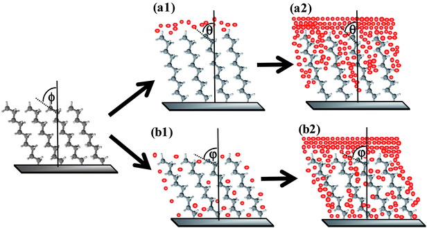 | ||
| Fig. 8 Hypothetical view of monolayer–metal interactions during gold deposition via (a) thermal evaporation and (b) physical vapour deposition. Φ, θ and φ are titled angles before and after metal deposition. Reprinted with permission from ref. 45. Copyright 2009 American Chemical Society. | ||
3.2 Indirect deposition
A conventional vacuum evaporator can be modified to protect substrates from direct exposure to the metal source.19–22 For example, deposition can be performed by flipping the sample stage 180° so that it is facing away from the evaporation source, or using a shutter in between the sample and source with a low back pressure of an inert gas (typically argon).19,34,55,69 In this case, particle energy and direct thermal radiation are no longer factors as the metal vapour within the vacuum chamber slowly condenses onto the modified substrate. An illustration of an indirect evaporation chamber is shown in Fig. 9,34 where the sample is facing away from the metal source and can be cooled during deposition in an atmosphere of back filled inert gas. This method has been examined in studies involving organic monolayers on both Si and GaAs.19,55,69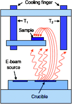 | ||
| Fig. 9 View of vacuum chamber for Indirect, cooled evaporation. Samples are placed on a holder either facing away from the crucible (as shown here) or a shutter is inserted between sample and source to block any direct line of sight between source and sample. Evaporation starts after reaching a base vacuum pressure, then filling the chamber with a low back pressure of inert gas and cooling the sample holder. A second cold finger with T2 < T1 assures that the sample will not be the coldest spot in the chamber, thereby reducing condensation of spurious gas residues. Reprinted from H. Haick and D. Cahen, Making contact: connecting molecules electrically to the macroscopic world, Prog. Surf. Sci., 2008, 83, 217–261. Copyright 2008, with permission from Elsevier. | ||
Indirect evaporation has been shown to preserve the quality of the Si bound monolayers upon Au deposition, firstly by Scott et al. in 2008.55 A follow-up report described that there is a clear difference in electrical performance when monolayers of different dipole moments are placed onto a Si wafer with Au deposited in this manner.22 In both studies, a different monolayer, terminated with substituted benzene rings, was used to construct the junction.19,22,55 The IR spectroscopic characterization clearly indicated that minimal monolayer-disruption occurs.19,55 As mentioned above, including a benzene ring into the monolayer structure can result in π-stacking with adjacent molecules, which stabilizes the monolayer and prevents metal penetration.64 Another study using indirect Au evaporation employed a thiol-terminated monolayer.14 Temperature dependent electrical measurements demonstrated similar effects of the monolayer using either a Hg metal contact or a deposited Au contact.14 Simple n-alkyl monolayers bound to GaAs have been reported to have different electrical characteristics than those with special head groups.70,71 It is reasonable to conclude that indirect evaporation aids in the prevention of damage to the molecular monolayer during the formation of a top metal contact.
3.3 Other techniques to form Au contacts
A number of other techniques to place Au contacts onto a molecularly modified semiconductor surface have yet to be attempted with Si substrates.33,34 Transfer printing, for example, involves the evaporation of a thin Au layer onto a polymer stamp. The contacts are then mechanically contacted with the organic film to form the junction. In order to keep the Au contacts on the surface, the formation of chemical bonds is necessary, and often achieved with Au–S bonds; in other words, the Au contact is placed on HS-terminated monolayers.3.4 Formation of multilayer metal contacts
Another approach that may prevent Au penetration into the monolayer is the deposition of “lighter” metals (with less kinetic energy during evaporation) such as titanium (Ti), palladium (Pd), or silver (Ag) onto the monolayer prior to Au deposition. These metals, specifically Ag, have been shown to cause less damage to the monolayer when thermally deposited. Fig. 10 (top plot) shows IR spectra of Au and (bottom plot) Ag (200 nm) deposited onto several organic monolayers synthesized from octadecyltrichlorosilane (“OTS”), 1-octadecene (“alkene”), 1-octadecanol (“alcohol”) and octadecanal (“aldehyde”).16 For Au contacts, a complete loss in carbon signal occurs for all but the OTS monolayer, while the monolayer signal is maintained for each monolayer in the bottom spectrum, where Ag is deposited.16 While Ag is highly conductive, it is also more reactive and prone to oxidation, causing degradation under ambient conditions, making electrical performance unreliable. Titanium is a particularly poor choice for metal–monolayer interfaces as it will react with the monolayer to form titanium carbide.72,73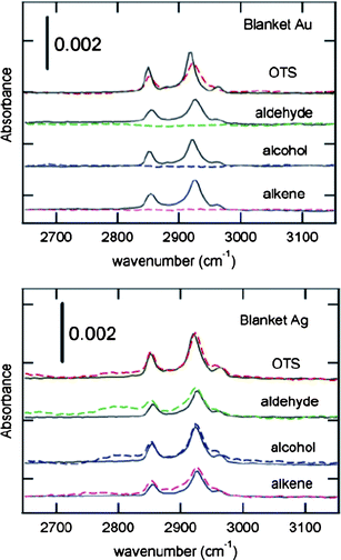 | ||
| Fig. 10 Infrared spectra of organic films under 200 nm of (top) Au and (bottom) Ag. After metal deposition, the resulting junction is a metal|monolayer|Si(111) junction, where the monolayer is constructed from: octadecyltrichlorosilane (“OTS”), 1-octadecene (“alkene”), 1-octadecanol (“alcohol”) and octadecanal (“aldehyde”). Solid lines are transmission spectra obtained prior to metallization and dashed lines are transmission spectra obtained after treating the backside to ensure that all samples have an identical organic-free entrance face. Reprinted with permission from ref. 16. Copyright 2007 American Chemical Society. | ||
Precautions can be made to limit the reactions of lighter metals if they are to be used in MMS construction, e.g., a thicker Au capping layer may be placed on top.12,24 However, Ag can form an alloy with Au, which creates an additional electronic medium and may unpredictably modify the electronic properties.74
Direct physical deposition techniques for Au contact formation onto modified Si substrates cause significant damage to the monolayer. Therefore, indirect metal evaporation appears to be one of the key improvements towards the use of vacuum deposition techniques to fabricate Au–M–Si junctions. Other deposition techniques may also be effective, such as transfer printing, which has yet to be attempted on organically modified Si. The use of metals such as Ag and copper (Cu) is also a possibility; however, their chemical stability is the main concern.
4. New approaches to prepare molecular diodes
Considering the limits and construction issues of the deposition techniques presented above, new methods for Au–M–Si construction have been investigated. A recent example is the construction of these junctions using flip-chip lamination (FCL), i.e., placing a monolayer onto Au pads, then binding the monolayer to Si.56,57 Using monolayers as ligands which bind to metal ions has been demonstrated in metal–organic frameworks and atomic layer deposition.24,66,67 This may serve as another method to place a protective metal layer prior to the deposition of Au onto a monolayer, using solution chemistry rather than physical deposition techniques.24,66,67 Fabrication of Au contacts independently of the modified silicon using modified polymer-assisted lift-off techniques (MoPALO) has recently been reported and appears to be effective in maintaining the overall integrity of Au–M–Si junctions.754.1 Flip-chip lamination
To make Au–M–Si junctions by flip-chip lamination (FCL), the preparation procedure is started at the opposite end of conventional construction methods. Fig. 11 shows a schematic of a FCL process reported by Coll et al. (2009)56 Starting with Au pads deposited onto a polymer surface (e.g. polyethylene terephthalate or PET), monolayers are constructed first on the Auviathiol chemistry, then reacted with a freshly prepared H–Si substrate viananotransfer printing.56,57 Devices constructed using this method have shown better stability at preserving the monolayer integrity even with an increase in temperature.56,57 A carboxylic acid head-group has been used and is shown to bond to H–Si substrate via the formation of RCOO–Si.56,57 Electrical characterization also finds a clear difference between junctions prepared with varied alkyl chain lengths.56,57 Transition voltage spectra (I/V2versus 1/V) from current–voltage characteristics indicate the degree of rectification of a diode. A comparison of three H–Si(111) n+ molecular diodes made with ultra smooth gold (via FCL with monolayers of 16-mercaptohexadecanoic acid (MHA), 11-mercaptoundecanoic acid (MUA) or a control (tungsten probe tip)) is shown in Fig. 12.56 The existence of monolayers is seen by the loss in linearly of the current–voltage characteristics (inset) as well as by the separation in the minima in each plot.
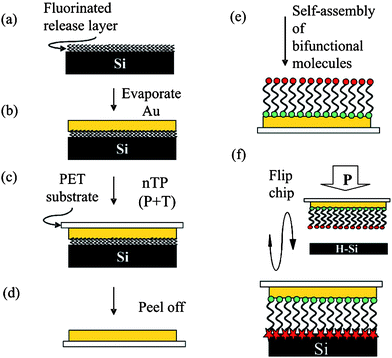 | ||
| Fig. 11 Schematic of flip-chip lamination process to form metal–molecule–silicon molecular junctions preserving the integrity of the molecules. Evaporated gold (b) is lifted off of a fluorinated release layer (a) onto a PET substrate by using nanotransfer printing (nTP) (c) to reveal the ultra-smooth Au underside (d). Bifunctional molecules are self-assembled onto ultra smooth gold forming a dense monolayer with the functional group exposed (e). Finally, the two electrodes are laminated together with nTP causing bonding between the exposed functional group and H–Si(111) (f). Reprinted with permission from ref. 56. Copyright 2009 American Chemical Society. | ||
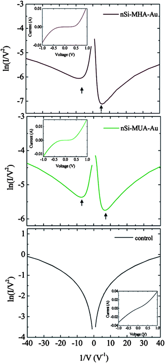 | ||
| Fig. 12 Transition voltage spectra of ultra smooth gold (uSAu)|MHA|Si molecular junctions (MHA: 16-mercaptohexadecanoic acid), uSAu|MUA|Si molecular junctions (MUA: 11-mercaptoundecanoic acid) and control (direct contact between a tungsten probe tip and H–Si(111)). Arrows indicate forward and reverse bias minima in MHA and MUA molecular junctions. Insets show the linear I–V plot for the respective junctions. Reprinted with permission from ref. 56. Copyright 2009 American Chemical Society. | ||
4.2 Using monolayer head-groups as metal ligands
The previous sections have highlighted the difficulties in the preparation of in reality, uniform Au–M–Si junctions using physically deposited Au contacts. Using head-groups which chelate with metals can provide nucleation sites for thin-film growth, a similar effect as forming Au–S bonds with above mentioned thiol head-groups. The use of other metal chelating head-groups besides those for Au may be advantageous as the ligand-like interaction they exhibit may provide a broader network of surface stability across the entire monolayer and may be more forgiving of monolayer defects. Fig. 13 shows a possible reaction process involving first a monolayer attached to the Au with a head-group which can act as a metal ligand.67 The metal ligand binds to a metal precursor which reacts with additional organic ligands and subsequent metal precursors in a layer by layer fashion. Once the metal ions are on the surface of an organic film they could, theoretically, be reduced into a metallic layer without interfering with the film integrity. Another possible interest might be in solution techniques to place the metal contacts onto the monolayer which are far less energetic than any vacuum deposition method currently in use. A review by Zacher et al. (2009) on metal–organic frameworks described a number of methods where monolayer head-groups on a variety of underlying substrates can coordinate to metal ions in solution.66 The metals could then be exposed to other coordinating organic molecules to create more complex molecular junctions.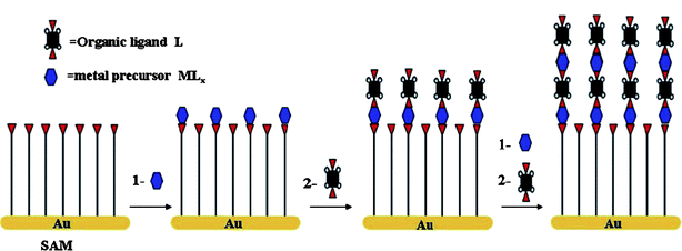 | ||
| Fig. 13 A schematic diagram for the step-by-step growth of metal–organic frameworks on self-assembled monolayers by repeated growth cycles separated by washing: first immersion in a solution of metal precursor and subsequently in a solution of the organic ligand. Here, for simplicity, the scheme simplifies the assumed structural complexity of the carboxylic acid coordination modes. Reprinted with permission from ref. 67. Copyright 2007 American Chemical Society. | ||
Atomic layer deposition (ALD) is similar to the formation of metal–organic frameworks as it involves the head-group of a monolayer acting as a ligand to a metal ion. This has been attempted using Cu bound to a monolayer terminated with carboxylic acid (–COOH) head-group.24 Although not all of the head-groups reacted with Cu+ when it was introduced, the ions clearly bound to the monolayer surface.24Fig. 14 is an absorption spectrum of the COOH-terminated SAM with Cu+ both unbound (a) and bound (b and c) to the ligand-like head-group.24 There are no significant shifts in the methylene stretching bands (2700–3000 cm−1) indicating the monolayer integrity is well maintained.24 Metal contacts can be grown on top of these monolayers to a desired thickness by repeating the ALD cycle, in order to create a stable Cu–M–Si junction.24 Once a layer of copper is bound to the monolayer, it can protect the monolayer integrity upon the deposition of destructive metals with conventional deposition techniques. Being at its early stages of development, the electrical performance of thus formed molecular junctions has not been reported.
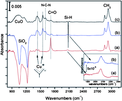 | ||
| Fig. 14 Absorption spectra of (a) COOH-terminated SAM and (b and c) COOH-terminated SAM with 20 Cu atomic layer deposition (ALD) cycles. (a) and (b) are referenced to the surfaces with the native oxide; (c) is referenced to the Si–H surface. Inset: magnified view of the Si–H region before and after the 20 Cu ALD cycles. The amount of hydrogen at the interface after the ALD cycles is equivalent to the one before ALD treatment. Reprinted with permission from ref. 24. Copyright 2009 American Chemical Society. | ||
4.3 Modified polymer-assisted lift-off technique (MoPALO)
The idea behind the recently reported MoPALO technique is essentially based on the lift-off float-on (LOFO) method.33,34,75 In the LOFO method, prepared metal contacts are detached from the substrate they are prepared on (glass slide or sacrificial substrates) into a detaching agent where they float on the surface and can then be picked up (e.g., by a modified silicon wafer).34 The new MoPALO technique, shown in Fig. 15, begins by depositing Au contacts onto a sacrificial mica substrate, followed by spin coating of a thin polyimide (PI) layer on top. Holes are made in the PI layer by photolithography to access the underlying Au contact. The PI/electrode film is detached from the mica into deionized water bath where it floats on the surface. The film can then be “floated” onto the desired substrate.75 In addition to this, permanent MoPALO (PeMoPALO) is also reported, where after photolithography, Au is deposited to both fill in the PI holes and to make external contact pads.75 The reported J–V measurements demonstrate that there is a chain-length dependence between Au|CH3(CH2)11–Si and Au|CH3(CH2)15–Si junctions for PeMoPALO junctions, but not for MoPALO junctions in the upper forward bias region.75 This difference is attributed to a better expression of tunnelling characteristics for smaller contacts over larger ones.75 This also clearly demonstrates that the monolayer integrity of the resulting Au–M–Si junctions is maintained through this method.
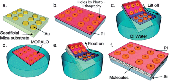 | ||
| Fig. 15 An illustrated modified polymer-assisted lift-off (MoPALO) process: (a) Au evaporation onto a sacrificial mica substrate; (b) spin-coated polyimide (PI), followed by photolithography to access Au through PI; (c) PI/Au film is removed from mica into a deionized (DI) water (“lift-off”); (d) floating PI/Au film in DI water; (e) PI/Au film is picked up (“float-on”) by the target substrate; and (f) Au|monolayer|Si junctions are created. Reprinted with permission from ref. 75. Copyright 2010 American Chemical Society. | ||
5. Conclusion
Results from various approaches used to form Au|monolayer|Si diodes have been reviewed. The ultimate goal is to form a gold contact on a continuous, molecular monolayer bonded to a Si surface, in such a manner that Si–Au interactions are prevented. Success is evaluated based on electrical contact properties, FTIR, XPS, Auger, mass spectroscopy, STM/BEEM, electron microscopy, and synchrotron-based techniques. It is clear that conventional Au deposition by direct physical methods (thermal evaporation or sputtering) disrupts organic monolayers bound to Si and does not provide the expected molecular junctions. The composition and packing density of the monolayer play a crucial role in protecting itself, regardless of the contact forming method. Indirect deposition causes less disruption to the monolayer, creating better performing junctions. The use of Au transfer printing shows potential for Au-contact construction on Si with little damage to the monolayer in comparison to other methods of fabrication. Using lighter metals (e.g., Ag, Ti, and Cr) before capping with an Au layer may be useful to reduce damage. However, these metals are prone to greater chemical interaction with the monolayer, forming carbides or experiencing oxidation under ambient conditions. New construction methods, flip-chip lamination, metal–organic frameworks, atomic-layer deposition, and modified polymer-assisted lift-off techniques have shown potential for having intact monolayers for the formation of molecular junctions.Acknowledgements
The authors greatly appreciate the financial support provided by the Natural Science and Engineering Research Council (NSERC) of Canada. R.P. wishes to thank Yeit-Ling Voon for editing the manuscript.References
-
W. Mönch, Electronic Properties of Semiconductor Interfaces, Springer-Verlag Berlin Heidelberg, Germany, 2004, vol. 43 Search PubMed
.
-
E. H. Rhoderick and R. H. Williams, Metal-Semiconductor Contacts, Clarendon Press, Oxford, 2nd edn, 1998, vol. 19 Search PubMed
-
S. M. Sze and K. K. Ng, Physics of Semiconductor Devices, John Wiley & Sons, Inc., Hoboken, New Jersey, 3rd edn, 2007 Search PubMed
- R. L. McCreery and A. J. Bergren, Adv. Mater., 2009, 21, 4303–4322 CrossRef CAS
- R. Hunger, W. Jaegermann, A. Merson, Y. Shapira, C. Pettenkofer and J. Rappich, J. Phys. Chem. B, 2006, 110, 15432–15441 CrossRef CAS
- R. K. Hiremath, B. G. Mulimani, M. K. Rabinal and I. M. Khazi, J. Phys.: Condens. Matter, 2007, 19, 446003 CrossRef
- M. Furuhashi, A. Omura, Y. Yamashita, K. Mukai, J. Yoshinobu, K. Akagi and S. Tsuneyuki, Jpn. J. Appl. Phys., 2009, 48, 055003 CrossRef
- F. Thieblemont, O. Seitz, A. Vilan, H. Cohen, E. Salomon, A. Kahn and D. Cahen, Adv. Mater., 2008, 20, 3931–3936 CrossRef CAS
- H. Z. Yu, S. Morin, D. D. M. Wayner, P. Allongue and C. H. de Villeneuve, J. Phys. Chem. B, 2000, 104, 11157–11161 CrossRef CAS
- Y. J. Liu and H. Z. Yu, ChemPhysChem, 2002, 3, 799–802 CrossRef CAS
- Y. J. Liu and H. Z. Yu, ChemPhysChem, 2003, 4, 335–342 CrossRef
- C. A. Richter, C. A. Hacker and L. J. Richter, J. Phys. Chem. B, 2005, 109, 21836–21841 CrossRef CAS
- M. A. Kuikka, W. J. Li, K. L. Kavanagh and H. Z. Yu, J. Phys. Chem. C, 2008, 112, 9081–9088 CrossRef CAS
- T. Böcking, A. Salomon, D. Cahen and J. J. Gooding, Langmuir, 2007, 23, 3236–3241 CrossRef
- A. Ng, S. Ciampi, M. James, J. B. Harper and J. J. Gooding, Langmuir, 2009, 25, 13934–13941 CrossRef CAS
- C. A. Hacker, C. A. Richter, N. Gergel-Hackett and L. J. Richter, J. Phys. Chem. C, 2007, 111, 9384–9392 CrossRef CAS
- W. Li, K. L. Kavanagh, C. M. Matzke, A. A. Talin, F. Léonard, S. Faleev and J. W. P. Hsu, J. Phys. Chem. B, 2005, 109, 6252–6256 CrossRef CAS
- Y. L. Loo, D. V. Lang, J. A. Rogers and J. W. P. Hsu, Nano Lett., 2003, 3, 913–917 CrossRef CAS
- H. Haick, O. Niitsoo, J. Ghabboun and D. Cahen, J. Phys. Chem. C, 2007, 111, 2318–2329 CrossRef CAS
- N. Gergel-Hackett, C. D. Zangmeister, C. A. Hacker, L. J. Richter and C. A. Richter, J. Am. Chem. Soc., 2008, 130, 4259–4261 CrossRef CAS
- A. Scott, D. B. Janes, C. Risko and M. A. Ratner, Appl. Phys. Lett., 2007, 91, 033508 CrossRef
- A. Scott, C. Risko, N. Valley, M. A. Ratner and D. B. Janes, J. Appl. Phys., 2010, 107, 024505 CrossRef
- D. K. Aswal, S. Lenfant, D. Guerin, J. V. Yakhmi and D. Vuillaume, Anal. Chim. Acta, 2006, 568, 84–108 CrossRef CAS
- O. Seitz, M. Dai, F. S. Aguirre-Tostado, R. M. Wallace and Y. J. Chabal, J. Am. Chem. Soc., 2009, 131, 18159–18167 CrossRef CAS
- H. Asanuma, G. P. Lopinski and H. Z. Yu, Langmuir, 2005, 21, 5013–5018 CrossRef CAS
- Y. J. Liu, D. M. Waugh and H. Z. Yu, Appl. Phys. Lett., 2002, 81, 4967–4969 CrossRef CAS
- F. Cleri, Appl. Phys. Lett., 2008, 92, 103112 CrossRef
- J. Zhao, Z. Huang, X. Yin, D. Wang and K. Uosaki, Phys. Chem. Chem. Phys., 2006, 8, 5653–5658 RSC
- W. Robison, R. Sharma and L. Eyring, Acta Metall. Mater., 1991, 39, 179–186 CrossRef CAS
- J. K. Bal and S. Hazra, Phys. Rev. B: Condens. Matter Mater. Phys., 2007, 211, 205411 CrossRef
- H. D. Hallen, A. Fernandez, T. Huang, R. A. Burhrman and J. Silcox, J. Vac. Sci. Technol., B, 1991, 9, 585–589 CrossRef CAS
- J. J. Yeh, J. Hwang, K. Bertness, D. J. Friedman, R. Cao and I. Lindau, Phys. Rev. Lett., 1993, 70, 3768–3771 CrossRef CAS
- H. Haick and D. Cahen, Acc. Chem. Res., 2008, 41, 359–366 CrossRef CAS
- H. Haick and D. Cahen, Prog. Surf. Sci., 2008, 83, 217–261 CrossRef CAS
- A. Hiraki, E. Lugujjo and J. W. Mayer, J. Appl. Phys., 1972, 43, 3643–3649 CrossRef CAS
- C. Siffert and A. Coche, IEEE Trans. Nucl. Sci., 1964, June, 244–248 CrossRef
- D. K. Aswal, C. Petit, G. Salace, D. Guérin, S. Lenfant, J. V. Yakhmi and D. Vuillaume, Phys. Status Solidi A, 2006, 203, 1464–1469 CrossRef CAS
- J. M. Buriak, Chem. Rev., 2002, 102, 1271–1308 CrossRef CAS
- D. D. M. Wayner and R. A. Wolkow, J. Chem. Soc., Perkin Trans. 2, 2002, 23–34 RSC
- L. Scheres, M. Giesbers and H. Zuilhof, Langmuir, 2010, 26, 4790–4795 CrossRef CAS
- R. Boukherroub and D. D. M. Wayner, J. Am. Chem. Soc., 1999, 121, 11513–11515 CrossRef CAS
- A. B. Sieval, R. Linke, H. Zuilhof and E. J. R. Sudhölter, Adv. Mater., 2000, 12, 1457–1460 CrossRef CAS
- Y. L. Liu, N. M. Navasero and H. Z. Yu, Langmuir, 2004, 20, 4039–4050 CrossRef CAS
- O. Seitz, T. Böcking, A. Salomon, J. J. Gooding and D. Cahen, Langmuir, 2006, 22, 6915–6922 CrossRef CAS
- H. Asanuma, H. Noguchi, Y. F. Huang, K. Uosaki and H. Z. Yu, J. Phys. Chem. C, 2009, 113, 21139–21146 CrossRef CAS
- R. T. W. Popoff, H. Asanuma and H. Z. Yu, J. Phys. Chem. C, 2010, 114, 10866–10872 CrossRef CAS
- R. Boukherroub, S. Morin, F. Bensebaa and D. D. M. Wayner, Langmuir, 1999, 15, 3831–3835 CrossRef CAS
- H. Asanuma, E. M. Bishop and H. Z. Yu, Electrochim. Acta, 2007, 52, 2913–2919 CrossRef CAS
- R. Boukherroub, S. Morin, P. Sharpe, D. D. M. Wayner and P. Allongue, Langmuir, 2000, 16, 7429–7434 CrossRef CAS
- L. Scheres, A. Arafat and H. Zuilhof, Langmuir, 2007, 23, 8343–8346 CrossRef CAS
- S. R. Puniredd, O. Assad and H. Haick, J. Am. Chem. Soc., 2008, 130, 9184–9185 CrossRef CAS
- E. J. Nemanick, P. T. Hurley, B. S. Brunschwig and N. S. Lewis, J. Phys. Chem. B, 2006, 110, 14800–14808 CrossRef CAS
- R. S. Puniredd, O. Assad and H. Haick, J. Am. Chem. Soc., 2008, 130, 13727–13734 CrossRef CAS
- A. B. Sieval, B. van den Hout, H. Zuilhof and E. J. R. Sudhölter, Langmuir, 2001, 17, 2172–2181 CrossRef CAS
- A. Scott, C. A. Hacker and D. B. Janes, J. Phys. Chem. C, 2008, 112, 14021–14026 CrossRef CAS
- M. Coll, L. H. Miller, L. J. Richter, D. R. Hines, O. D. Jurchescu, N. Gergel-Hackett, C. A. Richter and C. A. Hacker, J. Am. Chem. Soc., 2009, 131, 12451–12457 CrossRef CAS
- M. Coll, C. A. Richter and C. A. Hacker, J. Vac. Sci. Technol., B: Microelectron. Nanometer Struct.–Process., Meas., Phenom., 2009, 27, 2826–2831 Search PubMed
- J. P. Ponpon and P. Siffert, J. Appl. Phys., 1978, 49, 6004–6011 CrossRef CAS
- J. H. Kim, G. Yang, S. Yang and A. H. Weiss, Surf. Sci., 2001, 475, 37–46 CrossRef CAS
-
C. Chatgilialoglu, Organosilanes in Radical Chemistry, John Wiely & Sons, Inc., Hoboken, New Jersey, 2004 Search PubMed
- H. Asanuma, Y. J. Liu and H. Z. Yu, Jpn. J. Appl. Phys., 2005, 44, 1991–1993 CrossRef CAS
- L. Segev, A. Salomon, A. Natan, D. Cahen, L. Kronik, F. Amy, C. K. Chan and A. Kahn, Phys. Rev. B: Condens. Matter Mater. Phys., 2006, 74, 165323 CrossRef
- F. Buckel, F. Effenberger, C. Yan, A. Gölzhauser and M. Grunze, Adv. Mater., 2000, 12, 901–905 CrossRef CAS
- S. Maisch, F. Buckel and F. Effenberger, J. Am. Chem. Soc., 2005, 127, 17315–17322 CrossRef CAS
- J. C. W. Song, K. E. J. Goh, N. Chandrasekhar and C. Troadec, Phys. Rev. B: Condens. Matter Mater. Phys., 2009, 79, 165313 CrossRef
- D. Zacher, O. Shekhah, C. Wöll and R. A. Fischer, Chem. Soc. Rev., 2009, 38, 1418–1429 RSC
- O. Shekhah, H. Wang, S. Kowarik, F. Schreiber, M. Paulus, M. Tolan, C. Sternemann, F. Evers, D. Zacher, R. A. Fischer and C. Wöll, J. Am. Chem. Soc., 2007, 129, 15118–15119 CrossRef CAS
- E. H. G. Backus and M. Bonn, Chem. Phys. Lett., 2005, 412, 152–157 CrossRef CAS
- P. D. Carpenter, S. Lodha, D. B. Janes and A. V. Walker, Chem. Phys. Lett., 2009, 472, 220–223 CrossRef CAS
- S. Lodha and D. B. Janes, Appl. Phys. Lett., 2004, 85, 2809–2811 CrossRef CAS
- S. Lodha and D. B. Janes, J. Appl. Phys., 2006, 100, 024503 CrossRef
- B. de Boer, M. M. Frank, Y. J. Chabal, W. R. Jiang, E. Garfunkel and Z. Bao, Langmuir, 2004, 20, 1539–1542 CrossRef CAS
- K. Konstadinidis, P. Zhang, R. L. Opila and D. L. Allara, Surf. Sci., 1995, 338, 300–312 CrossRef CAS
- A. Hooper, G. L. Fisher, K. Konstadinidis, D. Jung, H. Nguyen, R. Opila, R. W. Collins, N. Winograd and D. L. Allara, J. Am. Chem. Soc., 1999, 121, 8052–8064 CrossRef CAS
- N. Stein, R. Korobko, O. Yaffe, R. H. Lavan, H. Shpaisman, E. Tirosh, A. Vilan and D. Cahen, J. Phys. Chem. C, 2010, 114, 12769–12776 CrossRef CAS
| This journal is © The Royal Society of Chemistry 2011 |