Synthesis of single crystalline CdS nanocombs and their application in photo-sensitive field emission switches†
Padmakar G.
Chavan
a,
Satish S.
Badadhe
b,
Imtiaz S.
Mulla
b,
Mahendra A.
More
a and
Dilip S.
Joag
*a
aCenter for Advanced Studies in Materials Science and Condensed Matter Physics, Department of Physics, University of Pune, Pune, 411 007, India. E-mail: dsj@physics.unipune.ac.in
bPhysical and Materials Chemistry Division, National Chemical Laboratory, Pune, 411 008, India
First published on 21st December 2010
Abstract
Single crystalline CdS nanocombs were synthesized by a thermal evaporation route. The photo-sensitive field emission current shows a reproducible switching behavior, with a rise in current level of nearly five times the initial preset value of ∼1 μA. An ultra low turn-on field, required to draw an emission current density of ∼0.1 μA cm−2 (100 nA), is found to be ∼0.26 V μm−1 (260 V), which is much lower than the reported values for various other CdS nanostructures. Upon illumination with visible light the CdS nanocombs act as a photo field emission switch. At an applied field of ∼0.65 V μm−1 the current densities are observed to be ∼14.6 μA cm−2 and ∼26.9 μA cm−2, without and with light illumination, respectively. The average emission current is seen to be stable over the duration of measurement for two preset values. The high sensitivity and fast response in the visible range indicates that the CdS nanocombs can be used as a photo-sensitive field emitting switch in device applications, and also in pulsed electron beam technology.
Introduction
Semiconducting chalcogenides in various nanoforms have gained importance1 in recent years due to their size and shape dependent physical properties.2 Amongst them is cadmium sulfide (CdS), a II–VI semiconductor, which has gained recognition as a promising material for light emitting diodes, solar cells and photoconductive devices by virtue of its photosensitive properties.3–7 In addition, owing to its controllable morphology and morphology dependent properties, it has been investigated as a field emission material.8 So far, field emission studies on CdS nanostructures have been aimed towards the synthesis of various morphologies by a variety of routes, the attainment of lower turn on voltages, higher current densities at lower fields, and better stability. However, until now, these studies have been rather limited as compared to other field emitters.9 Since CdS exhibits intrinsic photoconductivity, it is of scientific and technological interest to explore the photo-enhanced field emission behavior of its nanoforms.In the present work, we report the synthesis of CdS nanocombs by a simple thermal evaporation method on a silicon (Si) substrate and their photo-sensitive field emission behavior upon illumination with visible light. CdS nanocombs are grown on a Si substrate so that the application can be integrated with Si technology. The study demonstrates the potential application of CdS nanocomb emitters as a fast photo-sensitive switch. To the best of our knowledge this is the first report on fast switching photo-sensitive field emission of CdS nanocombs.
Experimental
Synthesis of CdS nanocombs
The method for the synthesis of single crystalline CdS nanocombs is based on thermal evaporation of high-purity CdS powder (99.99%, Alfa Aesar) under controlled conditions, using Au as a catalyst. An alumina boat, filled with appropriate amount of CdS powder was placed in the middle of the quartz tube of programmable temperature controlled furnace. The Au coated silicon substrate (1 cm × 1 cm) was kept at a distance of 29 cm downstream of the gas flow from the center. The CdS nanocomb morphology was observed only at this position on substrate, repetitively. The Si substrate was first ultrasonically cleaned in acetone for 20 min and then sputter-coated with a thin (∼30 Å) layer of Au film. Initially the reaction chamber was flushed with Ar, with a flow rate of 100 sccm (standard cubic centimeters per minute), for an hour followed by heating up to 1000 °C with a ramp of 20 °C min−1, and was kept at this temperature for 40 min with constant Ar flow of 250 sccm. After the furnace was cooled to room temperature, the Ar gas flow was turned off. A yellow wool-like product was found on the entire surface of the gold coated Si substrate. This as-synthesized product was used for further characterization.Characterization
The surface morphology of the CdS nanocombs was investigated by scanning electron microscopy (SEM) (JEOL 6360A), and the elemental composition was obtained using an energy-dispersive X-ray spectrometer (EDS) equipment attached to the SEM. The morphology and the crystalline nature of the as-synthesized product were further studied by transmission electron microscopy and high resolution transmission electron microscopy (TEM and HRTEM, Tecnai G2 20 Twin, FEI). For TEM studies, CdS nanocombs were scratched out of the Si surface and deposited on the carbon-coated Cu grid using analytical grade isopropyl alcohol. The phase identification of the as-synthesized product was obtained by X-ray diffraction (XRD, D8 Advance, Bruker AXS). The optical properties were investigated from photoluminescence (PL) spectra recorded at room temperature using a Xenon lamp as the excitation source (photoluminescence spectrometer; Perkin-Elmer-LS-55). The excitation wavelength used was 325 nm.The field emission current density versus applied field (J–E) and current versus time (I–t) characteristics were measured in a planar diode configuration at the base pressure of ∼1 × 10⁻⁸ mbar. The specimen (CdS nanocombs on Si substrate) was loaded in the ultra high vacuum chamber which served as a cathode, and a semi transparent phosphor screen as an anode. The cathode–anode assemblies were held parallel to each other with ∼1 mm separation. The field emission current was measured with the cathode at room temperature using an auto ranging Keithley 485 picoammeter and a Spellman high voltage DC power supply (0–40 kV, Spellman USA). Care was taken to avoid any current leakage by using shielded cables with proper grounding.
Results and discussion
Fig. 1 depicts the typical SEM images of CdS nanocombs. Fig. 1(a) indicates wide coverage of CdS nanocombs on the entire Si substrate. A magnified SEM image (Fig. 1(b)) and close up image (inset of Fig. 1(b)) clearly indicate the formation of nanocomb like structures which exhibit asymmetric growth of spikes under experimental conditions (ESI†). These spikes have a tip diameter of ∼200 nm and a length of a few micrometers. After scanning the entire surface of the specimen, it was clear that the growth of the CdS nanocombs is highly asymmetric. A recent study shows that the (0001)-Cd-terminated surface is chemically active and can be a self-catalyst for growing “comblike” or one-sided “saw teeth” structures.10 The composition of the CdS nanocombs was analyzed by EDS, and the pattern is shown in Fig. 1(c). Elemental analysis shows that the atomic ratio (Cd![[thin space (1/6-em)]](https://www.rsc.org/images/entities/char_2009.gif) :S) is ∼1:1, which is consistent with stoichiometric CdS within the experimental error.
:S) is ∼1:1, which is consistent with stoichiometric CdS within the experimental error.
 | ||
| Fig. 1 (a) An SEM image of as-synthesized CdS nanocombs grown on Si substrate, (b) a close up view of the CdS nanocombs and (c) EDS spectrum of the CdS nanocombs. | ||
The crystalline phase of the product and its crystallographic orientation were identified by X-ray diffraction (XRD) studies. Fig. 2 depicts the XRD of the CdS nanocombs synthesized by the simple thermal evaporation technique. All the reflection peaks can be indexed to the wurtzite CdS phase, with lattice constants a = 4.14 Å and c = 6.72 Å, consistent with the reported values (JCPDS Card No. 41-1049). This indicates that the CdS nanostructures crystallize in the pure wurtzite form, belonging to the space group P63mc, and show no evidence of a mixed phase of cubic symmetry. No diffraction peaks due to impurities and other phases, such as CdO, Cd, or S, were detected, indicating the high purity of the product.
 | ||
| Fig. 2 X-Ray diffraction pattern of CdS nanocombs. | ||
Photoluminescence (PL) spectroscopy is an effective method to evaluate the nature of transitions and defects in materials. Usually, two emission bands are observed for CdS nanostructures; excitonic and trapped state luminescence.11
The room temperature PL of the as-synthesized CdS nanocombs film measured in the spectral range of 470–750 nm is shown in Fig. 3. A prominent green emission band at ∼520 nm was seen, which is the characteristic emission of the bulk CdS. A similar peak was also reported by Kar et al.12 The absence of emission from the surface and deep states associated with the defects and impurities demonstrate that these single-crystal CdS nanocombs possess high quality optical properties and should be excellent building blocks for photonic devices.
 | ||
| Fig. 3 Photoluminescence spectrum recorded at room temperature. | ||
The morphology and the crystalline nature of the as-synthesized product were further confirmed by transmission electron microscopy (TEM). Fig. 4a shows a TEM image of a single CdS nanocomb exhibiting uniform length and smooth facets, and a corresponding selected area electron diffraction (SAED) pattern as the inset. The ripple like contrast on the CdS nanocomb (inset image) is due to the strain caused by bending of the nanoforms. For the TEM observation a sub micron size CdS comb was chosen. One representative high resolution HRTEM image of the CdS nanocomb is shown in Fig. 4b, with the corresponding fast Fourier transformed electron diffraction (FFTED) pattern as the inset. The high resolution TEM image reveals distinct lattice fringe spacing, ∼0.33 nm, which corresponds well to the (010) plane of CdS. From the HRTEM examination, it is found that no dislocations and planar defects, such as stacking faults and twins, exist in the nanocombs. The SAED pattern shown in the inset of Fig. 4a also indicates that the nanocombs are of a highly crystalline nature.
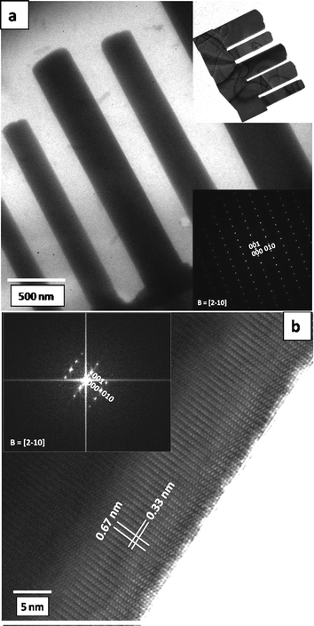 | ||
| Fig. 4 (a) A TEM image of a CdS nanocomb, insets are the TEM and SAED of the CdS nanocomb; (b) an HRTEM image of an individual nanocomb with the FFTED pattern as an inset. | ||
For the growth of micro/nanostructures in the vapor deposition system, two mechanisms have been proposed, namely the vapor–solid (VS)13 and vapor–liquid–solid (VLS)14 mechanisms. In our experiment, although Au is observed in the EDS pattern, the VLS mechanism can be ruled out because no metal (Au) particles were found in the structures of the tips of the CdS nanocomb (which is a finger-print of the VLS model). Hence we suggest that the VS mechanism is dominant in this case.15
The field emission current density-applied field (J–E) characteristic of the CdS nanocombs is depicted in Fig. 5a. As the field emission behaviour is directly dependent on the relative dimensions of the emitter, CdS nanocombs with fine nanospikes are expected to be good field emitters. The turn-on field, defined as the field required to draw an emission current density of ∼0.1 μA cm−2, is found to be ∼0.26 V μm−1. As the applied voltage is increased further, the emission current is found to increase very rapidly and an emission current density of ∼14.6 μA cm−2 is drawn at an applied field of ∼0.65 V μm−1. The observed value of the turn-on field is much higher than the values reported for CdS nanostructures by other researchers, as mentioned in the Table 1.6,16–20 The lowest value of the observed turn-on field is attributed to three essential factors. Firstly, CdS is a mid band gap semiconductor (2.4 eV), compared to ZnO (3.7 eV), so it is expected that the valence band electrons would tunnel out at a lower applied field than that required for the valence band electrons of ZnO. Secondly, there is a reduced screening effect in the case of the CdS nanocombs due to a sufficient spacing between the emitters, and thirdly, there is the nanometric dimension and high aspect ratio of the CdS nanocombs. The applied field E is defined as E = V/d, where V is the applied voltage and d is the separation between the emitter cathode and the anode. This field is also referred to as the average field. In the present case, the current density J is estimated by considering the entire area (1 cm2) of the emitter. The Fowler–Nordheim (FN) plot i.e. ln (J/E2) versus (1/E), derived from the observed J–E characteristic, is shown in Fig. 5b. The FN plot shows overall linear behavior, with a decrease in the slope (saturation tendency) in the high applied field range. This type of FN plot, exhibiting a tendency toward saturation at a high applied field, is consistent with previous reported results.6,21
 | ||
| Fig. 5 (a) A field emission current density-applied field (J–E) plot of the CdS nanocombs and (b) the corresponding Fowler-Nordheim (FN) plot. | ||
The current–time (I–t) plot recorded at a base pressure of 1 × 10⁻⁸ mbar is shown in Fig. 6. The emission current stability of the CdS nanocomb emitter has been investigated at the preset current values of ∼1 μA and ∼5 μA. The emission current in both the cases increases initially and is seen to stabilize later. This can be attributed to the preconditioning of the emitter as the field emission is a surface sensitive phenomenon and it requires preconditioning by removal of the adsorbed species. The average emission current is seen to be stable over the duration of the measurement, characterized by fluctuations in the form of “spikes”. The appearance of the “spikes” in the emission current is attributed to the adsorption, desorption, and migration of the residual gas molecules on the emitter surface. The striking feature of the field emission behavior of the CdS nanocomb emitter is that the average emission current remains nearly constant over the entire duration and shows no signs of degradation. The relative stability of the field emission current is expected to be related to the good contact between the Au/Si substrate and the CdS nanocombs. This is a remarkable feature, particularly from the point of view of an application as an electron source. Typical field emission images, captured at the different applied fields of ∼0.3 and ∼0.6 V μm−1, are shown as the inset of Fig. 6. The images show a number of tiny spots, corresponding to the emission from the most protruding CdS nanocombs. The temporal changes in the intensity of the spots are observed to be commensurate with the emission current fluctuation as seen in the I–t plot.
 | ||
| Fig. 6 Current versus time (I–t) plots of the CdS nanocombs, and an inset showing the FEM images taken at different applied fields. | ||
CdS is known to be a good photo-conductive semiconductor.22 In order to exploit its photoconductivity we have performed photo-sensitive field emission studies by exposing the cathode to a constant intensity of incident light. For these investigations, the cathode was illuminated from the ‘front side’ by keeping a halogen lamp (1300 W m−2) at a distance of ∼10 cm. The intensity of incident light was calibrated using a photocell and was found to be ∼80 W m−2 at the cathode surface. A plot of the photo-sensitive field emission current versus time is shown in Fig. 7a. It is seen that the emission current level increases instantly in the presence of light and it rapidly decreases to the original set value as the lamp is switched off. The rise in the current level is seen to be five times the initial preset value. This light-induced effect on the field emission current is observed to be reproducible. The observed photosensitivity can be attributed to the electrical photoconductivity resulting from the photo induced electrons, i.e. electrons from the valence band are excited into the conduction band creating additional charge carriers, thus increasing the photoconductivity. Whenever a material has an increased number of electrons in the conduction band due to excitations, the conductivity of that material will also increase, as seen in the linear equation for conductivity,
| σ = neμe (Ω m)−1 |
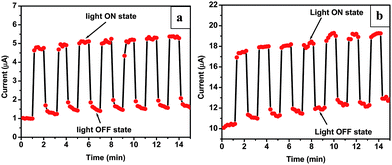 | ||
| Fig. 7 Photo switching behavior of the CdS nanocombs at preset current of ∼1 μA. shown in (a) and (b) at the preset current of ∼10 μA. | ||
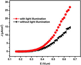 | ||
| Fig. 8 J–E plots of CdS nanocombs with and without light illumination. | ||
| Emitter | Mode of operation | Turn-on field/V μm−1 (for ∼0.1 μA cm−2) | Maximum current density (μA cm−2) (at a field of ∼0.65 V μm−1) |
|---|---|---|---|
| CdS nanocombs | Without illumination | 0.26 | 14.6 |
| With illumination | 0.24 | 26.9 |
 | ||
| Fig. 9 Schematic of the photo-sensitive field emission mechanism. | ||
In summary, we have studied the photo field emission switching properties of CdS nanocombs, which shows the possibility of fabricating a photo field emitter device which can be sensitive to visible light, acting as a switch. The CdS nanocombs are grown on a Si substrate and hence can be integrated with Si based technology.
Conclusion
Single crystalline CdS nanocombs are synthesized by a simple thermal evaporation technique. Field emission studies show CdS nanocombs are a suitable candidate for use as a cold electron source, having a very low turn-on field value ∼0.26 V μm−1 (current density ∼0.1 μA cm−2). These CdS nanocombs exhibit photo switching properties. Upon illumination, the rise in current is about five times the preset current value, which is remarkable. The switching behavior is quite reproducible. The enhancement in the emission current upon illumination is attributable to the photoconductivity of CdS.Acknowledgements
Padmakar Chavan is thankful to the UGC, India for the award of Rajiv Gandhi National Fellowship. D.S.J. and M.A.M. would like to thank UoP, Pune. We thank Mr. C. Narendraraj, NCL Pune, for his helpful discussion regarding SAED. The field emission work has been carried out as a part of the CNQS, UoP.References
- M. Law, D. Sirbuly, J. Johnson, J. Goldberger, R. Saykally and P. D. Yang, Science, 2004, 305, 1269 CrossRef CAS.
- J. Watt, N. Young, S. Haigh, A. Kirkland and R. D. Tilley, Adv. Mater., 2009, 21, 2288 CrossRef CAS.
- O. Hayden, A. B. Greytak and D. C. Bell, Adv. Mater., 2005, 17, 701 CrossRef CAS.
- I. Visoly-Fisher, S. R. Cohen, D. Cahen and C. S. Ferekides, Appl. Phys. Lett., 2003, 83, 4924 CrossRef CAS.
- N. Kouklin, L. Menon, A. Z. Wong, D. W. Thompson, J. A. Woollam, P. F. Williams and S. Bandyopadhyay, Appl. Phys. Lett., 2001, 79, 4423 CrossRef CAS.
- Y. F. Lin, Y. J. Hsu, S. Y. Lu and S. C. Kung, Chem. Commun., 2006, 2391 RSC.
- Z. H. Yin, Y. Z. Long, C. Z. Gu, M. X. Wan and J. L. Duvail, Nanoscale Res. Lett., 2009, 4, 63 CrossRef CAS.
- T. Zhai, X. Fang, Y. Bando, Q. Liao, X. Xu, H. Zeng, Y. Ma, J. Yao and D. Golberg, ACS Nano, 2009, 3, 949 CrossRef CAS.
- X. S. Fang, Y. Bando, U. K. Gautam, C. H. Ye and D. Golberg, J. Mater. Chem., 2008, 18, 509 RSC.
- Z. L. Wang, X. Y. Kong and J. M. Zuo, Phys. Rev. Lett., 2003, 91, 185502 CrossRef CAS.
- M. O'Nell, J. Marohn and G. McLendon, J. Phys. Chem., 1990, 94, 4356 CrossRef CAS.
- S. Kar and S. Chaudhuri, J. Phys. Chem. B, 2006, 110, 4542 CrossRef CAS.
- Z. W. Pan, Z. R. Dai and Z. L. Wang, Science, 2001, 291, 1947 CrossRef CAS.
- Y. N. Xia, P. D. Yang, Y. G. Sun, Y. Y. Wu, B. Mayers, B. Gates, Y. D. Yin, F. Kim and H. Q. Yan, Adv. Mater., 2003, 15, 353 CrossRef CAS.
- T. Zhai, X. Fang, Y. Bando, B. Dierre, B. Liu, H. Zeng, X. Xu, Y. Huang, X. Yuan, T. Sekiguchi and D. Golberg, Adv. Funct. Mater., 2009, 19, 2423 CrossRef CAS.
- M. Zhang, T. Zhai, X. Wang, Y. Ma and J. Yao, Cryst. Growth Des., 2010, 10, 3 CrossRef CAS.
- A. Datta, P. G. Chavan, F. J. Sheini, M. A. More, D. S. Joag and A. Patra, Cryst. Growth Des., 2009, 9, 4157 CrossRef CAS.
- H. Pan, C. Poh, K. Y. Zhu, G. Xing, K. C. Chin, Y. P. Feng, J. Lin, C. H. Sow, W. Ji and A. T. S. Wee, J. Phys. Chem. C, 2008, 112, 11227 CrossRef CAS.
- C. J. Lee, T. J. Lee, S. C. Lyu, Y. Zhang, H. Ruh and H. J. Lee, Appl. Phys. Lett., 2002, 81, 3648 CrossRef CAS.
- Q. Zhao, X. Y. Xu, X. F. Song, X. Z. Zhang, D. P. Yu, C. P. Li and L. Guo, Appl. Phys. Lett., 2006, 88, 033102 CrossRef.
- J. H. Park, P. S. Alegaonkar, S. Y. Jeon and J. B. Yoo, Compos. Sci. Technol., 2008, 68, 753 CrossRef CAS.
- K. Colbow and D. W. Nyberrg, J. Phys. Chem. Solids, 1968, 29, 509 CrossRef CAS.
- J. Milam, J. Allen and L. Lauhon, Nanoscape, 2005, 2, 1 Search PubMed.
- R. B. Sharma, R. A. Singh, G. C. Dubey, V. N. Tondare, N. Pradeep and D. S. Joag, Mater. Sci. Eng., A, 2003, 353, 52 CrossRef.
- F. J. Sheini, M. A. More, S. R. Jadkar, K. R. Patil, V. K. Pillai and D. S. Joag, J. Phys. Chem. C, 2010, 114(9), 3843 CrossRef CAS.
Footnote |
| † Electronic supplementary information (ESI) available. See DOI: 10.1039/c0nr00659a |
| This journal is © The Royal Society of Chemistry 2011 |