DOI:
10.1039/C0NR00623H
(Paper)
Nanoscale, 2011,
3, 1246-1251
Raman scattering by confined optical phonons in Si and Ge nanostructures
Received
25th August 2010
, Accepted 8th November 2010
First published on 27th January 2011
Abstract
A microscopic theory of the Raman scattering based on the local bond-polarizability model is presented and applied to the analysis of phonon confinement in porous silicon and porous germanium, as well as nanowire structures. Within the linear response approximation, the Raman shift intensity is calculated by means of the displacement–displacement Green's function and the Born model, including central and non-central interatomic forces. For the porous case, the supercell method is used and ordered pores are produced by removing columns of Si or Ge atoms from their crystalline structures. This microscopic theory predicts a remarkable shift of the highest-frequency of first-order Raman peaks towards lower energies, in comparison with the crystalline case. This shift is discussed within the quantum confinement framework and quantitatively compared with the experimental results obtained from porous silicon samples, which were produced by anodizing p−-type (001)-oriented crystalline Si wafers in a hydrofluoric acid bath.
1. Introduction
During the last decade great research efforts have been focused on the nanostructured monoatomic semiconductors, such as porous silicon (PSi), porous germanium (PGe) and the nanowire structures. Silicon is the second most abundant element in the earth's crust and nowadays is the base of microelectronics. In contrast, Ge has a large dielectric constant and is particularly suitable for photonic crystal applications. However, these two traditional semiconductors have indirect electronic band gaps, i.e. optical transitions require the assistance of phonons. This disadvantage seems to be overcome in their nanostructured counterpart. For example, a strong room-temperature photoluminescence in the visible range is observed in PSi1 and recently in PGe.2 In general, the nanostructured materials present two unusual features: (1) an extremely high ratio of surface area to unit volume, which could lead to potent chemical catalysts as well as ultrasensitive gas and biological sensors, and (2) a significant reduction of system size reaching the nanometre scale—then the energy levels of most elementary excitations become discrete enough to be measured at a macroscopic scale. In fact, a deeper understanding of nanostructured materials could be essential to the search for novel technological applications.
Among a widespread list of optical characterization methods, the Raman spectroscopy is an inelastic and non-destructive technique made to study elementary excitations in solids and to determine the nanoparticle size and symmetry.3–6 The Raman scattering in solids is a complex process, in which an incident photon is absorbed by an electron through an interband transition and some of these excited electrons could emit or absorb a phonon or other bosons before they return to the valence band, emitting a photon with a lower or higher energy than the incident one, respectively corresponding to Stokes and anti-Stokes scatterings. Actually, one can renormalize the coordinates of electron and visualize the Raman spectroscopy as a scattering of photons by emission or absorption of phonons.7 Given that the wavevector of photons in the visible range (∼1/5000 Å−1) is much smaller than the first Brillouin zone (∼1 Å−1) of phonons, the momentum conservation law only allows the participation of optical phonons close to the zone centre, since acoustical phonons at the same zone have energies almost null, being less than 1 cm−1. In a nanostructured material, this restriction is relaxed and the Raman response is generally enhanced. In this paper, we present a microscopic theory of the Raman scattering based on the bond-polarizability model and linear response approximation. This theory is applied to the study of the optical-phonon confinement in PSi, PGe and nanowires. The calculations are carried out by means of the displacement–displacement Green's function and the Born potential, including central and non-central nearest-neighbor interatomic interactions. The theoretical prediction about a notable shift of the highest-frequency of first-order Raman peaks towards lower energies is verified in PSi samples and a good agreement is found.
2. Theory of Raman scattering
The Raman scattering in solids is a long-wavelength measurement of the fluctuation in the dielectric function and its spectral intensity is determined by the imaginary part of the dynamic correlation function of local dielectric constants.8 From the polarization tensor developed by Albenet al.,9 the local bond polarizability [α(j)] can be assumed to be linear with the atomic displacement [uμ(j)], i.e. cμ(j) = ∂α(j)/∂uμ(j) is a constant and alternates only the sign from site to site in a single crystal with diamond structure. Hence, the Raman response [R(ω)] at zero temperature can be written within the linear response theory as8,10| |  | (1) |
where i and j are the index of atoms, μ and μ′ = x, y, or z stand Cartesian coordinates, and Gμ μ′(i,j,ω) is the displacement–displacement Green's function determined by the Dyson equationwhere M is the atomic mass of Si or Ge, I stands for the matrix identity, and Φ is the dynamic matrix, whose elements are given by| |  | (3) |
There are several interatomic interaction potentials able to reproduce reasonably well the phonon band structure of covalent semiconductors, such as the Keating,11 Stillinger–Weber,12 and Tersoff13 models. In this article, let us consider a simple interaction potential (Vij) between nearest-neighbor atoms i and j as given in the Born model14
| |  | (4) |
where
u(
i) is the displacement of atom
i with respect to its equilibrium position, and
α and
β are, respectively, the central and non-central restoring force constants. The unitary vector
![[n with combining circumflex]](https://www.rsc.org/images/entities/b_char_006e_0302.gif) ij
ij indicates the bond direction between atoms
i and
j. The Born model has the advantage of being simple, containing only two parameters, and correctly reproduce the optical phonon band of crystalline silicon (
c-Si) and crystalline germanium (
c-Ge) around the center of Brillouin zone, as shown in
Fig. 1(a). This fact is particularly important for the analysis of quantum confinement effects on the highest-frequency first-order Raman response.
 |
| | Fig. 1 (a) Calculated phonon band structures of c-Si (orange solid lines) and c-Ge (green solid lines) compared with experimental data for c-Si (open circles) and c-Ge (solid spheres). (b) The calculated Raman spectra from eqn (1) are shown. Inset: interaction matrices (ϕn) in a tetrahedral structure. | |
3. Numerical results
The Raman spectra [R(ω)] are calculated for Si and Ge by using the Born model, whose nearest-neighbor interaction parameters are summarized in Table 1.14
Table 1 Central (α) and non-central (β) restoring force constants
| Born parameters |
Silicon
|
Germanium
|
|
α (N m−1) |
120.3 |
95.7 |
|
β (N m−1) |
23.5 |
24.4 |
These parameters are obtained by comparing the theoretical phonon dispersion relations, solid lines in Fig. 1(a) for c-Si and c-Ge, with the inelastic neutron scattering data15,16 illustrated in the same figure by orange open circles for c-Si and green solid spheres for c-Ge. The corresponding Raman spectra, calculated from eqn (1) using a primitive cell of two atoms, are shown in Fig. 1(b). Notice that the optical phonon bands are reasonably reproduced in comparison with the experimental data and they are responsible for the Raman scattering. The Raman peaks of c-Si and c-Ge are respectively located at ωSi = 519.3 cm−1,15 and ωGe = 300.2 cm−1,17 which correspond to optical phonons from the center of Brillouin zone, since the momentum conservation law only allows the participation of vibrational modes around the Γ point.
The porous semiconductors can be modeled by means of the supercell technique,18 in which columns of Si or Ge atoms are removed along [001] direction, as shown in the inset (a) of Fig. 2 for a supercell of 648 atoms, obtained by adding 9 × 9 cubic unit cells of eight atoms each on the xy plane, and 145 atoms of them were removed to produce this square columnar pore. The use of supercells with periodic boundary conditions in the three directions creates foldings of the first Brillouin zone and then there are several active Raman modes at the Γ point.19
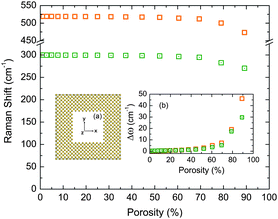 |
| | Fig. 2 Variation of the highest-frequency first-order Raman peaks (ωR) as a function of the porosity for square pores of Si (orange open squares) and Ge (green dotted squares). Insets: (a) z-axis view of square-pore supercell, and (b) Δω = ω0 − ωRversus the porosity, being ω0 = ωSi or ωGe. | |
The highest frequency of first-order Raman peaks (ωR) is plotted as a function of the porosity in Fig. 2 for ordered square pores of Si (orange open squares) and Ge (green dotted squares) in a supercell of 648 atoms, while its shift (Δω ≡ ω0 − ωR) with respect to the crystalline case (ω0), being ω0 = ωSi or ωGe, is shown in the inset (b) of Fig. 2, where the porosity is defined as the ratio of the removed atom number over the original number of atoms in the supercell. We observe that ωR is almost a constant for the low porosity region and has a notable variation when the porosity is larger than 60%, i.e. when the distance between nearest-neighbor pores (d) is smaller than 2aSi = 10.86 Å or 2aGe = 11.3 Å. This behavior can be understood within the quantum confinement framework as follows: the presence of pores introduces extra nodes to the phonon wavefunctions allowing only wave lengths smaller than d, which produces a shift of ωRtowards lower frequency whose value can be approximately determined by the optical phonon dispersion relation ω(q) of Fig. 1(a) evaluated at wavevector |q| ≈ 2π/d. It would be worth emphasizing that this phonon confinement is derived from extended vibrational states.
We have also calculated ωRfor rhombic pores. The main characteristics and results of calculated supercells of 648 atoms with square and rhombic columnar pores are respectively summarized in Tables 2 and 3, while their shapes are illustrated in the insets of Fig. 2 and 3.
 |
| | Fig. 3 The shift Δω = ω0 − ωRversus the inverse of squared quasi-confinement distance (d), being ω0 = ωSi or ωGe. Insets: top-view of a nanowire and four supercells with rhombic pores, where d is illustrated for both cases. | |
Table 2 Description and Raman shifts of square pores in a supercell of 648 atoms
| Removed atoms |
8 |
18 |
32 |
50 |
72 |
98 |
128 |
162 |
| Porosity (%) |
1.23 |
2.77 |
4.93 |
7.71 |
11.11 |
15.12 |
19.75 |
25.0 |
|
Si
|
ω
R (cm−1) |
519.15 |
519.10 |
519.05 |
518.98 |
518.90 |
518.80 |
518.66 |
518.47 |
|
Ge
|
ω
R (cm−1) |
299.76 |
299.72 |
299.68 |
299.62 |
299.56 |
299.52 |
299.44 |
299.32 |
| Removed atoms |
200 |
242 |
288 |
338 |
392 |
450 |
512 |
578 |
| Porosity (%) |
30.86 |
37.34 |
44.44 |
52.16 |
60.49 |
69.44 |
79.01 |
89.19 |
|
Si
|
ω
R (cm−1) |
518.21 |
517.84 |
517.26 |
516.32 |
514.20 |
512.02 |
503.92 |
475.76 |
|
Ge
|
ω
R (cm−1) |
299.12 |
298.88 |
298.52 |
297.88 |
296.50 |
294.80 |
288.60 |
270.37 |
Table 3 Description and Raman shifts of rhombic pores in a supercell of 648 atoms
| Removed atoms |
4 |
9 |
25 |
49 |
81 |
121 |
169 |
225 |
289 |
| Porosity (%) |
0.61 |
1.38 |
3.85 |
7.56 |
12.5 |
18.67 |
26.08 |
34.72 |
44.59 |
|
Si
|
d (nm) |
6.3353 |
6.1433 |
5.7593 |
5.3754 |
4.9914 |
4.6075 |
4.2235 |
3.8395 |
3.4556 |
|
ω
R (cm−1) |
519.15 |
519.10 |
519.05 |
518.98 |
518.90 |
518.80 |
518.66 |
518.47 |
518.21 |
|
Ge
|
d (nm) |
6.7917 |
6.5920 |
6.1924 |
5.7929 |
5.3934 |
4.9939 |
4.5944 |
4.1949 |
3.7954 |
|
ω
R (cm−1) |
300.08 |
300.06 |
300.02 |
299.96 |
299.88 |
299.78 |
299.64 |
299.48 |
299.27 |
In Fig. 3, the shift Δω for rhombic pores in Si (orange open rhombuses) and Ge (green dotted rhombuses) is plotted as functions of the inverse of squared confinement distance (d), which is illustrated in the inset of Fig. 3. Observe that for both Si and Ge systems the results of porous semiconductors reveal an almost linear relationship, in accordance with the quantum confinement framework, and both lines intersect to the horizontal axis around 0.02, which is related to the used supercell size of 648 atoms. For the limiting case of an infinite supercell, this intersection would be at zero. Notice also that these lines are not straight, since there is a kind of quantum confinement originated by extra nodes in the wavefunctions at the boundaries of pores,18 contrast to the nanowire results where the quantum confinement is complete in the xy plane. There is in addition a natural connection between both results, since the porous systems loss the space connectivity on the xy plane when the vertexes of rhombic pores touch each other.
In Table 4 the main features and results of studied Si and Ge nanowires are summarized, where we start from a cubic supercell of eight atoms and take the periodic boundary condition along the z-axis and free one in x and y directions. Atomic layers are further added in these directions to obtain nanowires with larger cross-section. For porous systems, Fig. 4(a) presents the normalized shift (ωR/ω0) as a function of the porosity for square pores in Si (orange open squares) and Ge (green dotted squares) in comparison with nanowires by plotting ωR/ω0versus the confinement distance (d) shown in Fig. 4(b) for square nanowires of Si (orange solid squares) and Ge (green half-filled squares). Observe that for both pore and wire systems the confinement effects are stronger in Ge than in Si, possibly related to the fact that βGe > βSi.
 |
| | Fig. 4 (a) The normalized shift (ωR/ω0) versus the porosity for square pores of Si (orange open squares) and Ge (green dotted squares), and (b) ωR/ω0versus confinement distance (d), defined in its inset, for nanowires of Si (orange solid squares) and Ge (green half-filled squares). | |
Table 4 Description and Raman shifts of square nanowires
| Unit-cell atom number |
8 |
18 |
32 |
50 |
72 |
98 |
128 |
|
Si
|
d (nm) |
0.4072 |
0.6787 |
0.9502 |
1.2217 |
1.4932 |
1.7647 |
2.0360 |
|
ω
R (cm−1) |
474.5 |
497.3 |
506.5 |
511 |
513.5 |
515.0 |
516.0 |
|
Ge
|
d (nm) |
0.4237 |
0.7062 |
0.9887 |
1.2712 |
1.5537 |
1.8362 |
2.1187 |
|
ω
R (cm−1) |
269.8 |
285.2 |
291.2 |
294.2 |
295.9 |
296.9 |
297.6 |
| Unit-cell atom number |
162 |
200 |
242 |
288 |
338 |
392 |
450 |
|
Si
|
d (nm) |
2.3077 |
2.5792 |
2.8507 |
3.1222 |
3.3937 |
3.6652 |
3.9367 |
|
ω
R (cm−1) |
516.7 |
517.2 |
517.5 |
517.8 |
518.0 |
518.2 |
518.4 |
|
Ge
|
d (nm) |
2.4012 |
2.6837 |
2.9662 |
3.2487 |
3.5312 |
3.8137 |
4.0963 |
|
ω
R (cm−1) |
298.0 |
298.4 |
298.6 |
298.8 |
298.9 |
299.0 |
299.24 |
4. Experimental setup
PSi samples were fabricated by an electrochemical anodization of p−-type (100)-oriented c-Si wafers with an electrical resistivity of 6–12 Ω cm in a 1![[thin space (1/6-em)]](https://www.rsc.org/images/entities/char_2009.gif) :1:2:1 HF:H2O:ethanol(C2H5OH):glycerol(C3H8O3) solution, which was recycled by a mechanical pump to remove air bubbles generated by the electrochemical reaction and to improve the homogeneity of PSi films.20 In order to ensure electrical conduction during the anodization, a gold film was deposited on the backside of c-Si substrate. These samples were dried with pentane that diminishes the fracture of pore structures.21 The anodization parameters and some structural properties are summarized in Table 5, where the PSi film thickness (d) was determined by means of Leica/Cambridge (Stereoscan 440) Scanning Electron Microscope (SEM) operated at 20 kV and the sample's porosity (P) has been gravimetrically measured by using Mettler-Toledo XP105 analytical balance with a resolution of 0.01 mg and the following equation22
:1:2:1 HF:H2O:ethanol(C2H5OH):glycerol(C3H8O3) solution, which was recycled by a mechanical pump to remove air bubbles generated by the electrochemical reaction and to improve the homogeneity of PSi films.20 In order to ensure electrical conduction during the anodization, a gold film was deposited on the backside of c-Si substrate. These samples were dried with pentane that diminishes the fracture of pore structures.21 The anodization parameters and some structural properties are summarized in Table 5, where the PSi film thickness (d) was determined by means of Leica/Cambridge (Stereoscan 440) Scanning Electron Microscope (SEM) operated at 20 kV and the sample's porosity (P) has been gravimetrically measured by using Mettler-Toledo XP105 analytical balance with a resolution of 0.01 mg and the following equation22| |  | (5) |
where Δm is the dissolved mass determined by weighing the sample before and after the anodization, A (in cm2) is the area exposed to the electrolyte and ρSi is the density of c-Si. In addition, all the samples contain a protective thin film of 75 nm over the PSi films, obtained by etching at beginning for 30 s with a current density of 5 mA cm−2, in order to avoid cracks of the p−-type PSi films.23 The measured sample porosities of Table 5 are slightly smaller than those found in ref. 24, perhaps due to the presence of the protective thin film as well as the use of glycerol in the anodization solution.
Table 5 Anodic-etching conditions and structural properties
| Sample |
Current density (mA cm−2) |
Anodization time (s) |
Film thickness (μm) |
Porosity (%) |
| I |
5 |
600 |
1.5 |
51.9 |
| II |
10 |
600 |
4.5 |
64.3 |
| III |
20 |
600 |
5.7 |
77.1 |
| IV |
30 |
600 |
8.0 |
84.6 |
Raman scattering spectra were measured with a Nicolet Almega XR dispersive micro-Raman spectrometer equipped with a 35 mW laser excitation at 532 nm. The measurements were performed at room temperature with a resolution of 1 cm−1 over the spectral range from 1598 to 443 cm−1 with a laser spot diameter of 25 μm.
In Fig. 5, Raman spectra are shown for c-Si, samples II and IV, where a notable shift of the Raman peak toward lower energy is observed. At the same time, the Raman peaks broaden as it shifts, in agreement with that observed in ref. 24. In particular, the anodization time of 600 s was chosen, since it leads to a thickness of PSi films so that the participation of c-Si substrate on the Raman spectra of PSi samples is negligible, except for sample I in which the etching rate at 5 mA cm−2 is very low, leading to a thinner PSi film.
 |
| | Fig. 5
Raman spectra of samples II (green open triangles) and IV (purple open circles) are compared with that of c-Si (orange spheres). | |
Fig. 6 shows the Raman peak position for samples I to IV as well as for c-Si in comparison with those of Fig. 2 for PSi with square pores. The error bars indicate the dispersion of measured micro-Raman peaks at different regions on each sample. Notice that the Raman shift of sample I is almost the same as for c-Si, since for a porosity of about 50% the quantum confinement effects on the optical phonons are relatively small as revealed by the theoretical analysis. Also, a possible participation of c-Si substrate to the Raman response should be considered, due to the smaller thickness of the PSi film in this sample.
 |
| | Fig. 6 The Raman peaks for c-Si and for samples I to IV (blue open circles) in comparison with the theoretical ones of Fig. 2 (orange open squares). Inset: the Raman spectrum of sample III (blue open circles) is compared with the theoretical results (orange open squares). | |
In the inset of Fig. 6, the Raman spectrum of sample III is compared with the theoretical Raman response obtained from a square pore of 544 atoms removed, i.e. 32 atoms on two adjacent sides of the pore surface were additionally removed from a square pore of 512 atoms in Table 2. These theoretical results include an imaginary part of energy of 7 cm−1, which produces a full width at half maximum (FWHM) of 14 cm−1, in order to include the structural disorder and thermal effects on the Raman spectra. An additional weighting function of exp(−|ω − ω0|/ξ) with ω0 = 497 cm−1 and ξ = 13 cm −1 is considered to eliminate spurious Raman peaks at lower energies due to the use of the supercell technique, since the artificial periodic boundary condition (absent in the real samples) leads to the appearance of many active Raman modes at the Γ point as a consequence of the folding processes of the first phonon Brillouin zone in the reciprocal space.19 In other words, in a porous sample the phonon momentum selection rule is relaxed due to the topological disorder and confinement effects, i.e. the complete Brillouin zone could be active for the Raman scattering. However, their relative contribution should diminish as the phonon momentum goes away from the center of the Brillouin zone and this fact might be included through an exponential weighting function.
6. Conclusions
We have presented a microscopic theory to model the Raman scattering in Si and Ge nanostructures. This theory has the advantage of providing a direct relationship between the microscopic structures and the Raman spectra. For PSi and PGe, contrary to the crystallite approach, the supercell model emphasizes the interconnection of the system, which could be relevant for long-range correlated phenomena, such as the Raman scattering. However, there is a weak point of the supercell technique, which creates foldings of the first Brillouin zone leading to the appearance of several spurious Raman peaks. Furthermore, the present calculation has been performed without passivating dangling bonds on the surface nither including structural relaxations. However, the phonon confinement effects on the Raman response seem to be reproduced by the present model and quantitatively acceptable in accordance to the experimental data. Calculations including the surface passivation and reconstruction can be carried out by using the density functional theory.25
Both theoretical and experimental results show a notable confinement effect on ωRand the variation Δω is in agreement with the effective mass theory. In particular, the measured Raman spectrum of Fig. 6 is in accordance with the calculated one. In fact, the theoretical porous system of the inset in Fig. 6 has a porosity of 83.9%, which is larger than the experimental one of 77.1%. This difference could be related to the formation of oxide layer on the pore surface.26 It would be worth mentioning that the p−-type PSi samples are easily fractured and we have tried to shield the porous structure by adding a protective low-porosity thin film, using glycerol in the etching solution, as well as pentane during the drying process. The analysis presented in this article can be extended to study other nanostructured semiconductors, such as nanotubes and quantum dots.
Acknowledgements
This work was partially supported by projects IN114008 from Universidad Nacional Autónoma de México (UNAM), 20090652 from SIP of Instituto Politécnico Nacional, 58938 and 25231-F from Consejo Nacional de Ciencia y Tecnología of México. The micro-Raman equipment of CCADT-UNAM and supercomputing facilities of DGSCA-UNAM are fully acknowledged.
Notes and references
- L. T. Canham, Appl. Phys. Lett., 1990, 57, 1046–1049 CrossRef CAS.
- C. Jing, C. Zhang, X. Zhang, W. Zhou, W. Bai, T. Lin and J. Chu, Sci. Technol. Adv. Mater., 2009, 10, 065001 CrossRef.
- I. H. Campbell and P. M. Fauchet, Solid State Commun., 1986, 58, 739–741 CrossRef CAS.
- G. Gouadec and P. Colomban, J. Raman Spectrosc., 2007, 38, 598–603 CrossRef CAS.
- A. K. Arora, M. Rajalakshmi, T. R. Ravindran and V. Sivasubramanian, J. Raman Spectrosc., 2007, 38, 604–617 CrossRef CAS.
- A. G. Rolo and M. I. Vasilevskiy, J. Raman Spectrosc., 2007, 38, 618–633 CrossRef CAS.
-
P. Y. Yu and M. Cardona, Fundamentals of semiconductors – physics and materials properties, Springer-Verlag, Berlin, 1996, pp 362 Search PubMed.
- R. M. Martin and F. L. Galeener, Phys. Rev. B, 1981, 23, 3071–3081 CrossRef CAS.
- R. Alben, D. Weaire, J. E. Smith and M. H. Brodsky, Phys. Rev. B: Solid State, 1975, 11, 2271–2296 CrossRef CAS.
- R. J. Elliott, J. A. Krumhansl and P. L. Leath, Rev. Mod. Phys., 1974, 46, 465–543 CrossRef.
- P. N. Keating, Phys. Rev., 1966, 145, 637–645 CrossRef CAS.
- F. H. Stillinger and T. A. Weber, Phys. Rev. B, 1985, 31, 5262–5271 CrossRef CAS.
- J. Tersoff, Phys. Rev. Lett., 1986, 56, 632–635 CrossRef CAS.
-
V. J. Torres and A. M. Stoneham, Handbook of interatomic potentials III. Semiconductors, Atomic Energy Research Establishment, Harwell, England, 1985 Search PubMed.
-
R. Hull, Properties of crystalline silicon, (Emis Series, INSPEC, London, 2000), pp. 159 Search PubMed.
- G. Nilsson and G. Nelin, Phys. Rev. B: Solid State, 1971, 3, 364–369 CrossRef.
- C. E. Finlayson, A. Amezcua-Correa, P. J. A. Sazio, N. F. Baril and J. V. Badding, Appl. Phys. Lett., 2007, 90, 132110 CrossRef.
- M. Cruz, C. Wang, M. R. Beltrán and J. Tagüeña-Martínez, Phys. Rev. B: Condens. Matter, 1996, 53, 3827–3832 CrossRef CAS.
- P. Alfaro, M. Cruz and C. Wang, IEEE Trans. Nanotechnol., 2006, 5, 466–468 CrossRef.
- R. Cisneros, C. Ramirez and C. Wang, J. Phys.: Condens. Matter, 2007, 19, 395010 CrossRef.
- D. Bellet and L. Canham, Adv. Mater., 1998, 10, 487–490 CAS.
-
V. Lehmann, Electrochemistry of silicon: instrumentation, science, materials and applications, Wiley-VCH Verlag, Weinheim, 2002, pp. 109 Search PubMed.
- J. Dian, A. Macek, D. Nižňanský, I. Němec, V. Vrkoslav, T. Chvojka and I. Jelínek, Appl. Surf. Sci., 2004, 238, 169–174 CrossRef CAS.
- G. Irmer, J. Raman Spectrosc., 2007, 38, 634–646 CrossRef CAS.
- Y. Bonder and C. Wang, J. Appl. Phys., 2006, 100, 044319 CrossRef.
- R. Cisneros, H. Pfeiffer and C. Wang, Nanoscale Res. Lett., 2010, 5, 686–691 CrossRef CAS.
|
| This journal is © The Royal Society of Chemistry 2011 |
Click here to see how this site uses Cookies. View our privacy policy here.