Transparent electrode requirements for thin film solar cell modules
Michael W.
Rowell
and
Michael D.
McGehee
*
Department of Materials Science and Engineering, Stanford University, Stanford, CA 94305, USA. E-mail: mmcgehee@stanford.edu; Fax: +1 650 725-4034; Tel: +1 650 723-2534
First published on 5th November 2010
Abstract
The transparent conductor (TC) layer in thin film solar cell modules has a significant impact on the power conversion efficiency. Reflection, absorption, resistive losses and lost active area either from the scribed interconnect region in monolithically integrated modules or from the shadow losses of a metal grid in standard modules typically reduce the efficiency by 10–25%. Here, we perform calculations to show that a competitive TC must have a transparency of at least 90% at a sheet resistance of less than 10 Ω/sq (conductivity/absorptivity ≥ 1 Ω−1) for monolithically integrated modules. For standard modules, losses are much lower and the performance of alternative lower cost TC materials may already be sufficient to replace conducting oxides in this geometry.
Broader contextHigh power conversion efficiency and the use of abundant materials are critical to the adoption of photovoltaic power at scale. The transparent conductor (TC) layer is a necessary component of all thin film solar cells and it has a significant impact on efficiency, resulting in a 10–25% power loss even for the best TCs. In the last several years there has been renewed interest in this area with the development of several new transparent and conductive oxides and nanostructured materials, many with the potential for both cost and performance advantages. For the development or adoption of any new TC material, it is useful to know the impact on efficiency and the necessary TC performance requirements. Here, we compare the two different ways of manufacturing thin film solar cells and quantify the transparent electrode related losses for a TC material of any performance and we specify the material figure of merit necessary for a TC material to be a compelling candidate for photovoltaic applications. |
Thin film solar cell modules can be manufactured either as a series of individual standard cells strung together in a fashion similar to silicon wafer based solar modules or as a series of cells monolithically interconnected during the film deposition process (Fig. 1). For both architectures, the top electrode has a significant impact on the efficiency and much of this reduction in efficiency is due to trade-offs associated with the transparent conductor (TC) material. Making the TC thin to increase its transmittance to light raises resistive losses. Making the finger spacing or electrode width narrow to reduce resistive losses causes a larger fraction of the module area to be composed of dead space, where the dead space is either shadow losses under the metal grid for standard cells or the interconnect scribe area for monolithically interconnected cells.
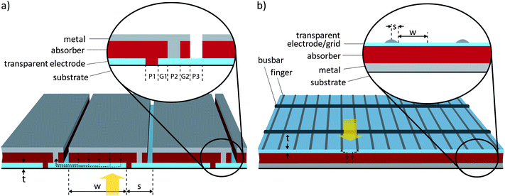 | ||
| Fig. 1 a) Cross section of a monolithically integrated thin film module. Only the active area of width w contributes to the power generation and the interconnect area of width s is lost area. Photogenerated current, denoted by the dashed lines, is injected into the transparent electrode and then driven laterally to one edge of the device where contact to the back metal electrode of the adjacent device is made. b) Cross section of a standard cell using metal grid/TC. Area under the grid lines is lost area and photogenerated current between the lines is conducted laterally over a short distance by the TC film. | ||
Monolithic integration is advantageous in that it eliminates the need to handle and assemble individual cells and thereby reduces manufacturing costs. A drawback, however, is that parasitic losses associated with the TC layer are more significant for monolithic modules—typically 15–25%.1 For standard modules employing large cells covered with a metal grid reinforced TC, losses are typically 10–15%. For both architectures, typically high quality sputtered transparent conducting oxides (TCO),2 such as indium tin oxide (ITO) or doped zinc oxide (ZnO), are used owing to their high conductivity and low absorptivity. Several new systems being investigated for use as the TC, including carbon nanotubes,3–7graphene,8–10nanowires11,12 and metal thin films,13 have the potential for both reductions in cost and gains in performance relative to TCOs.
Here, we calculate the total losses due to the limitations of the TC for a solar cell that has a nominal (“lab scale”) efficiency of 10%. For monolithically integrated thin-film modules, we show that a TC performance of at least 90% transmission, T, with a sheet resistance (Rsh) less than 10 Ω/sq is important. While higher TC performance will result in meaningful efficiency gains, lower TC performance will have a precipitous effect on efficiency. For standard modules employing a metal grid reinforced TC over large area cells, losses are much lower and improvements in TC performance will only result in marginal gains in efficiency. Alternative lower cost TC materials may already be sufficient to replace TCOs in this geometry.
Fig. 1 shows a cross section of both monolithically integrated thin film cells and a standard thin film cell employing a metal grid/TC as the transparent electrode. In monolithic modules, typically each cell is ∼1 cm wide and runs the length of the module. A module that is ∼1 m wide will then have on the order of 100 cells connected in series. The interconnect region, often referred to as “dead space”, does not contribute to the photocurrent and so the width of this region is kept as small as possible. The dead space width, labeled s in Fig. 1, cannot be infinitely narrow, however, due to both limitations in scribing technology and requirements for good isolation and a low resistance series connection between adjacent cells.14 In the commercialized thin film market, which is dominated by CdTe, CIGS and amorphous Si, the scribing is typically performed with laser processing,15 though mechanical scribing has also been demonstrated in the case of CdTe and CIGS where the semiconducting layer is only weakly adhered.16 Scribe widths, labeled P1–3 in Fig. 1, can be as narrow as 25 μm, but 50–150 μm is typical. Similarly, the gap between scribe lines, labeled G1–2, can be very narrow but limited accuracy in registry between scribe lines means gaps are typically 50–150 μm.17–19,20 With these restrictions, s can be 140–1000 μm and is typically 500 μm. In the case of solution processed TCs and active layers, such as organic semiconductors, it may be advantageous to eliminate the scribe processing steps and rely on printing to define the interconnect region. In this case, the limitations on s will likely be different.
Standard modules are made of individual cells stacked adjacent to one another and serially connected in a long string. The cells are typically on the order of 6 inches square and the front electrode consists of both a TC layer and a metal grid deposited with a low cost technique such as screen printing or inkjet printing of a metal paste that is then sintered. The grid normally consists of fine parallel lines (fingers) crossed by two thicker bus bars that collect current from the fingers and then make a serial connection to the adjacent cell. Ideally the grid lines are narrow and tall such that shadow losses are minimized and the line resistance is low. Typically the finger lines cannot be economically deposited at a width less than 130 μm and the busbar lines are ∼2 mm wide.21
For either module architecture, there is an optimum film thickness and device width, w, or finger spacing, 2w, that minimizes the net losses from the scribe or shadow area, the TC absorption and the TC sheet resistance. Calculating the fraction of power lost due to the scribe area and the TC absorption is straightforward. Accurately estimating the power loss due to the sheet resistance is more difficult. For small power losses, i.e. in the limit where the voltage variation in the transparent electrode is so small that the current injection across the device can be considered uniform, the fraction of power lost due to the TC sheet resistance can be reasonably predicted by estimating the Joule heating losses in the TC layer, Pload, relative to the nominal output power of the cell,5P0:
 | (1) |
 | (2) |
Fig. 2a shows the fraction of the nominal efficiency, η/η0, for monolithically integrated panels plotted as a function of w for ITO25 and two hypothetical materials that are 10 times better or 10 times worse (as defined by the σ/α figure of merit for TCs26,27 discussed below). For all of these plots the dead space, s, is fixed at 500 μm and an optimum thickness, t, has been found for each material. Typical values for jsc, Voc and the fill factor, FF, (20 mA cm−2, 0.71 V and 0.71, respectively) have been chosen such that the nominal (“lab cell”) efficiency is 10%. These plots show the trade-off between increasing the fraction of active area versus lowering the resistive losses in the TC. For ITO, the optimum film thickness is 195 nm and the optimal device width (w + s) is approximately 0.7 cm. Even at this optimum condition the efficiency is only 84% of the nominal efficiency. For the common device structure using glass–ITO there is an additional 2–3% reflection loss at the glass–ITO interface28 and additional reflection at the second ITO interface depending on the dielectric constant of the layer on top of the ITO. For the hypothetical material that is 10 times better, η/η0 reaches 91% at a width of 1.1 cm. And for the material that is 10 times worse, η/η0 reaches 71% at a width of 0.25 cm.
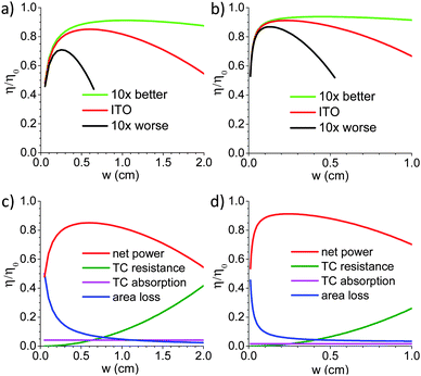 | ||
| Fig. 2 Fraction of nominal efficiency for three materials as a function of width, w, for monolithic (a) and standard (b) modules. For ITO, the fraction of nominal efficiency is re-plotted along with the three contributing losses due to TC sheet resistance, TC absorption and scribe area for monolithic (c) or shadow area for standard (d) modules. | ||
The loss in efficiency from a grid/TC for standard cells can similarly be calculated from eqn (1) under the assumption that the dominant series resistance contribution is due to the sheet resistance of the TC material between the fingers. Fig. 2 (b) shows the fraction of nominal efficiency for a finger width, 2s, fixed at 130 μm and a busbar width of 2 mm and spacing of 8 cm.21 For the materials shown in Fig. 1, the maximum fraction of nominal efficiency for the material 10 times better than ITO is 94% at an optimum TC film thickness and an optimum finger spacing (2w) of 9 mm. For ITO and a material 10 times worse, the maximum fraction of nominal efficiency is 91% and 87% at a finger spacing (2w) of 5 mm and 2.5 mm, respectively. For finger spacing much larger or finger width much smaller than the values given here, the resistive loss in the finger itself may be significant and adding busbars or controlling the aspect ratio of the grid lines will be critical.
The smaller efficiency loss for standard modules in comparison with the monolithically integrated configuration is an important factor in considering the advantages and disadvantages of these two different solar module manufacturing techniques. Significantly, the requirement for σ/α of the TC material for standard modules is less critical and so materials other than high performance TCOs may be compelling.
In Fig. 2 (c)–(d), the individual losses are plotted along with the net power for the same materials in Fig. 2 (a). At narrow widths the scribe loss becomes significant and at greater widths the resistive losses dominate. Comparing the three materials, the importance of the finite scribe width is apparent. If, for example, s could be reduced by half, this would nearly compensate for a 10 times change in the TC performance. It should also be noted that the resistance losses plotted here are for the specific solar cell parameters listed above, and from eqn (1) or (2), the resistance losses are seen to scale with jsc/Voc. For ITO, doubling the current to 40 mA cm−2, for example, will increase the total losses to ∼20%. For multijunction solar cells with lower current and higher voltage, however, losses will be lower.
For TC materials, the most direct figure of merit for ranking the performance of a TC is σ/α, given by eqn (3),
 | (3) |
While σ/α describes the performance of a TC material and can be used to rank the potential of different materials, the relationship between σ/α and η/η0 is non-linear. Fig. 3, shows the maximum η/η0 (optimized w and t) as a function of σ/α for the same limits on s used in Fig. 2 for both monolithic and standard integration. As σ/α drops below a value of ∼1 (equivalent to ∼90% T and 10 Ω/sq), the efficiency drops off rapidly. For σ/α much greater than 2, the efficiency continues to increase but less rapidly. For monolithically integrated solar modules, it is clear that for any TC material to be compelling as the transparent electrode, σ/α must be high enough to achieve at least 90% T and 10 Ω/sq (σ/α ≥ 1 Ω−1). For standard cells, the optimum TC film thickness is much less and so that the impact of the TC material is reduced. Even for materials as much as 10 times worse than TCOs, the loss in efficiency will be less than 15%, which may be an acceptable trade-off for alternative materials with cost or other benefits.
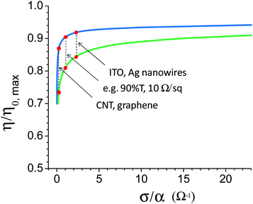 | ||
| Fig. 3 Maximum fraction of nominal efficiency as a function of the TC material figure of merit for monolithic integration (lower green line) and for standard integration (upper blue line). For monolithic integrations, achieving high module efficiencies will require σ/α ≥ 1 Ω−1, which corresponds to a performance equivalent to at least 90% T and 10 Ω/sq. | ||
Figure of merit values as high as 7 Ω−1 have been reported for TCOs,26 but this is predicted to be near the upper limit for TCOs.29 Recently much effort has been directed towards the use of nanostructured materials for transparent electrodes.30
Materials such as carbon nanotubes and graphene have shown promise but performance to date has been much lower than TCOs due to high intertube31 or intersheet resistances which greatly reduce the film mobility. The individual tubes or sheets have much higher electron mobility than TCOs, however, and so the upper limit for their performance may be significantly higher.9,10,32
In the last few years, films made of Ag nanowires11 or printed microgrids33 have achieved performance comparable to TCOs and the upper limit for these systems would seem to be much higher.11 In these systems, relying on nanostructures enables one to shrink the open space between the wires to the point where very little or no TC material is required in the open space. Often, a window layer such as CdS or conductive polymer is sufficiently conductive and the network acts as a homogeneous conductor. With further developments in this area, cutting the losses due to the TC by as much as 40% for monolithic modules and 30% for standard modules would seem to be within reach.
Acknowledgements
This publication was based on work supported by the Center for Advanced Molecular Photovoltaics (Award No KUS-C1-015-21), made by King Abdullah University of Science and Technology (KAUST).Notes and references
- A. V. Shah, H. Schade, M. Vanecek, J. Meier, E. Vallat-Sauvain, N. Wyrsch, U. Kroll, C. Droz and J. Bailat, Progr. Photovolt.: Res. Appl., 2004, 12, 113–142 Search PubMed.
- E. Fortunato, D. Ginley, H. Hosono and D. C. Paine, Mrs Bulletin, 2007, 32, 242–247 CAS.
- A. D. Pasquier, H. E. Unalan, A. Kanwal, S. Miller and M. Chhowalla, Appl. Phys. Lett., 2005, 87, 203511–203513 CrossRef.
- J. van de Lagemaat, T. M. Barnes, G. Rumbles, S. E. Shaheen, T. J. Coutts, C. Weeks, I. Levitsky, J. Peltola and P. Glatkowski, Applied Physics Letters, 2006, 88.
- M. W. Rowell, T.M.A., M. D. McGehee, H. J. Prall, G. Dennler, N. S. Sariciftci, L. Hu and G. Gruner, Appl. Phys. Lett., 2006, 88, 233506 CrossRef.
- Z. C. Wu, Z. H. Chen, X. Du, J. M. Logan, J. Sippel, M. Nikolou, K. Kamaras, J. R. Reynolds, D. B. Tanner, A. F. Hebard and A. G. Rinzler, Science, 2004, 305, 1273–1276 CrossRef CAS.
- R. C. Tenent, T. M. Barnes, J. D. Bergeson, A. J. Ferguson, B. To, L. M. Gedvilas, M. J. Heben and J. L. Blackburn, Adv. Mater., 2009, 21, 3210 CrossRef CAS.
- S. Bae, H. S. Kim, Y. Lee, X. Xu, J. S. Park, Y. Zheng, T. L. Balakrishnan, H. R. Kim, Y. I. Song, Y. J. Kim, K. S. Kim, J. H. A. Ozyilmaz, B. H. Hong and S. Iijima, Nat. Nanotechnol., 2010, 5, 574 CrossRef CAS.
- J. B. Wu, M. Agrawal, H. A. Becerril, Z. N. Bao, Z. F. Liu, Y. S. Chen and P. Peumans, ACS Nano, 2010, 4, 43–48 CrossRef CAS.
- S. De and J. N. Coleman, ACS Nano, 4, 2713–2720 Search PubMed.
- J. Y. Lee, S. T. Connor, Y. Cui and P. Peumans, Nano Lett., 2008, 8, 689–692 CrossRef CAS.
- R. Noriega, J. Rivnay, L. Goris, D. Kalblein, H. Klauk, K. Kern, L. M. Thompson, A. C. Palke, J. F. Stebbins, J. R. Jokisaari, G. Kusinski and A. Salleo, Journal of Applied Physics, 2010, 107.
- B. O'Connor, C. Haughn, K. H. An, K. P. Pipe and M. Shtein, Applied Physics Letters, 2008, 93.
- K. Brecl, M. Topic and F. Smole, Progr. Photovolt.: Res. Appl., 2005, 13, 297–310 Search PubMed.
- S. Nakano, T. Matsuoka, S. Kiyama, H. Kawata, N. Nakamura, Y. Nakashima, S. Tsuda, H. Nishiwaki, M. Ohnishi, I. Nagaoka and Y. Kuwano, Japanese Journal of Applied Physics Part 1-Regular Papers Short Notes & Review Papers, 1986, 25, 1936–1943 Search PubMed.
- D. Bonnet, Thin Solid Films, 2000, 361, 547–552 CrossRef.
- M. Powalla, G. Voorwinden, D. Hariskos, P. Jackson and R. Kniese, Thin Solid Films, 2009, 517, 2111–2114 CrossRef CAS.
- S. Yoo, W. J. Potscavage, B. Domercq, J. Kim, J. Holt and B. Kippelen, Applied Physics Letters, 2006, 89.
- C. Lungenschmied, G. Dennler, H. Neugebauer, S. N. Sariciftci, M. Glatthaar, T. Meyer and A. Meyer, Sol. Energy Mater. Sol. Cells, 2007, 91, 379–384 CrossRef CAS.
- Some thin film solar cells use a window layer or interface modifier (e.g. CdS (ref. 17) or PEDOT: PSS (ref. 18) which can be very conductive and so scribing must be done after this second layer is deposited or the gap must be made sufficiently wide to avoid shunting between adjacent cells. Furthermore, materials such as CdTe or CIGS can be fairly conductive themselves, in which case P1 must be sufficiently wide or scribing can be performed after the semiconductor deposition and the gap filled prior to deposition of the second electrode.
- D. H. Neuhaus and A. Munzer, Advances in OptoElectronics, 2007, 2007.
- G. T. Koishiyev and J. R. Sites, Sol. Energy Mater. Sol. Cells, 2009, 93, 350–354 CrossRef CAS.
- Note that when both the absorption spectrum of the solar cell and the absorption spectrum of the TC in consideration are known, the TC losses should be integrated over the solar spectrum.
- M. Agrawal and P. Peumans, Opt. Express, 2008, 16, 5385–5396 CrossRef.
- The conductivity of ITO (Sorizon Technologies) was calculated from sheet resistance (van der Pauw method: 20 Ω/sq) and thickness measurements (atomic force microscopy: 110 nm). The index of refraction and extinction coefficient were measured with an ellipsometer. Values were taken at 550 nm.
- R. G. Gordon, Mrs Bulletin, 2000, 25, 52–57 CAS.
- For each line in Fig. 2 an optimum thickness has been used in each case. This way it does not matter if the conductivity is changed or if the absorptivity is changed. Only the ratio conductivity
![[hair space]](https://www.rsc.org/images/entities/char_200a.gif) /absorptivity matters.
/absorptivity matters. - G. F. Burkhard, E. T. Hoke, S. R. Scully and M. D. McGehee, Nano Lett., 2009, 9, 4037–4041 CrossRef CAS.
- J. R. Bellingham, W. A. Phillips and C. J. Adkins, J. Mater. Sci. Lett., 1992, 11, 263–265 CrossRef CAS.
- A. Kumar and C. W. Zhou, ACS Nano, 4, 11–14 Search PubMed.
- P. N. Nirmalraj, P. E. Lyons, S. De, J. N. Coleman and J. J. Boland, Nano Lett., 2009, 9, 3890–3895 CrossRef CAS.
- L. F. C. Pereira, C. G. Rocha, A. Latge, J. N. Coleman and M. S. Ferreira, Applied Physics Letters, 2009, 95.
- K. Tvingstedt and O. Inganas, Adv. Mater., 2007, 19, 2893 CrossRef CAS.
| This journal is © The Royal Society of Chemistry 2011 |