 Open Access Article
Recent advances in semiconductor nanowire heterostructures
Jonas
Johansson
*a and
Kimberly A.
Dick
ab
aSolid State Physics, Lund University, Box 118, S-221 00, Lund, Sweden. E-mail: jonas.johansson@ftf.lth.se
bPolymer & Materials Chemistry, Lund University, Box 124, S-221 00, Lund, Sweden
First published on 14th September 2011
Abstract
Semiconductor nanowires have made a deep impact on materials science related research, and are being explored for applications in several disciplines. Many of these applications require heterostructures, which can be defined as the combination of two or more materials within the same nanowire structure. In this paper we briefly review the current state-of-the-art concerning epitaxial nanowire heterostructures. We discuss growth, understanding, and promising applications of such structures, which we divide into three categories: nanowire–substrate, axial, and radial heterostructures. For each of these categories, we review recent experimental results, and address possible difficulties and how they have been resolved. In addition, we also highlight interesting applications relying on heterostructures in nanowires. To illustrate that nanowires and their heterostructures have been grown in a plethora of materials, we pick examples from a wide range of semiconductor materials.
 Jonas Johansson | Jonas Johansson is Associate Professor at the Division of Solid State Physics at Lund University in Sweden, where he also received his M.Sc. in Chemical Engineering in 1996 and his Ph.D. degree in Solid State Physics in 2000. During 2003 he worked as a Post-Doctorate Researcher at the University of Copenhagen, Denmark. In the beginning of 2004 he returned to Lund University and started his research on nanowires. He is currently interested in modeling the formation mechanisms of nanowires with a focus on polytypism and heterostructures. Another research interest is thermodynamics of small systems. |
 Kimberly A. Dick | Kimberly A. Dick is Assistant Professor in Solid State Physics and in Polymer & Materials Chemistry at Lund University, Lund, Sweden, where she also received her Ph.D. degree in 2007. She completed undergraduate studies in Chemical Physics at University of Waterloo (Waterloo, Canada) in 2003. Her research focuses on nanostructure fabrication and structural characterization, with particular interest in fundamental growth processes. Current research focuses on semiconductor nanowires, with specific topics of interest including crystal phase engineering and design of antimonide-based heterostructures. |
Introduction
Semiconductor nanowires can be described as quasi-one-dimensional pieces of semiconductor material with diameters in the 10–100 nm range and lengths of the order of micrometres. Nanowires have made a strong impact in electronics as a promising route to further downscaling and extensions of Moore's law, in photovoltaics as promising solar cell materials, and in optoelectronics as highly efficient light emitting diodes. Several examples of these applications are already being considered for commercialization. Additionally, many more applications can be anticipated in life-sciences and in sensor structures.There are several methods to fabricate semiconductor nanowires and excellent reviews of different methods are given in ref. 1 and 2. In this highlight, we focus on growth of vertically aligned nanowires with epitaxial orientation to the substrate. This is the most technologically interesting class of nanowires, which offers the highest degree of control over the growth process. The favored growth direction for nanowires is {111}. For III–V semiconductors, the group V terminated {111} direction, {111}B (or its hexagonal counterpart) is favorable. Thus, to ensure growth of vertically aligned, epitaxial nanowires, a substrate with the same orientation as the nanowire growth direction should be used.
There are essentially two methods to grow vertically aligned epitaxial nanowires: (i) metal particle seeded growth and (ii) selective area growth. Here, we briefly outline these methods.
(i) Metal particle seeded growth
The first step is to pattern a (piece of a) semiconductor wafer (the substrate) with metal particles. There are a few different ways to do this.3 The most prominent methods are to deposit colloidal or aerosol fabricated particles or to define the metal particles by means of lithography, metal evaporation, and lift-off. The former methods result in randomly distributed metal particles and the latter in position controlled arrays of metal particles. After metal patterning, the substrate is transferred to an epitaxy reactor, typically metal organic vapor phase epitaxy (MOVPE) or molecular beam epitaxy (MBE). By increasing the temperature and introducing the reactant gases, the metal particle first forms an equilibrium alloy with one or more reactants. If the ambient supersaturation is high enough, the alloy particle becomes supersaturated. When the alloy supersaturation is high enough, semiconductor material dissolved in the metal particle precipitates in a layer-by-layer fashion at the interface between the particle and the substrate. The precipitated material constitutes the growing nanowire that lifts the metal particle as it grows. The diameter of the nanowire is dictated by the diameter of the metal alloy particle. The most commonly used metal, which works excellently for most nanowire materials systems is gold.4This growth mechanism is often, and sometimes for purely historical reasons, referred to as VLS (vapor-liquid-solid) growth,5 since these three phases are involved. However, in many materials systems, nanowires grow from solid particles, hence the term VSS (vapor-solid-solid) is sometimes seen. A unified discussion of growth mechanisms is given in ref. 6. A version of metal particle seeded growth where one or more of the nanowire elements (such as the group III metal of III–V nanowires) constitutes the seed particle is often referred to as self-seeded growth.
Metal particle seeded nanowire growth competes with growth from the vapor phase, which results in 2D film growth on the substrate and the nanowire side walls, leading to tapering. Thus, conditions to maximize nanowire growth over film growth have to be realized. A common strategy is to grow nanowires at temperatures where film growth is suppressed, often a couple of hundred degrees lower than optimum film growth temperatures.
(ii) Selective area growth
The idea is to partially mask the substrate so that material only grows at specific areas where the substrate is exposed. The first step is to fabricate a mask. This is often achieved by depositing an oxide or nitride layer on the substrate and then by lithographically opening holes in this mask. After masking, the substrate is transferred to an epitaxy reactor (most often MOVPE or MBE). After increasing the temperature and introducing the reactant gases, semiconductor material nucleate in the mask openings. By choosing appropriate growth conditions, these nuclei can develop into highly anisotropic structures where the lateral growth rate is orders of magnitude smaller than the axial growth rate. In some III–V materials systems it is not clear whether the growth proceeds by vapor phase deposition or if a metal particle of the group III constituent is present and assists the unidirectional growth [see self-seeded growth in (i) above]. It is important to use growth conditions, reactant flows and temperature, so that epitaxial lateral overgrowth (ELOG) is avoided and unidirectional nanowire growth is preferred. This growth mechanism is sometimes also referred to as catalyst-free growth.It is commonly claimed that one of the major advantages of nanowires is the seemingly endless possibilities to form heterostructures in nanowires as compared to in epitaxial films. In heterostructures, two or more materials are grown on top of each other; schematic illustrations of the three relevant categories of heterostructures are shown in Fig. 1. In Fig. 1a a heterocombination where the nanowire and the substrate are of different materials is shown, in Fig. 1b an axial, or longitudinal, heterostructures is shown, and in Fig. 1c, a radial, or core/shell, heterostructure is shown. The major advantage with heterostructures is that different materials have different bandgaps and this is something that is heavily utilized in modern electronics and optoelectronics applications. Design and fabrication based on combinations of different materials with different bandgaps is known as bandgap engineering.
 | ||
| Fig. 1 Simple schematic illustrations of nanowire heterostructures. The two different colors represent two different materials. (a) Nanowire–substrate heterostructure. (b) Example of an axial heterostructure. (c) Example of a radial heterostructure. Metal seed particles and nanowire sidewall faceting are omitted. The substrate is only shown in (a), where it is part of the heterostructure. | ||
In this short review, we will highlight some recent advances of nanowire heterostructures. We will put the emphasis on fundamental materials science but we will also show interesting applications. Our focus is on general aspects of nanowire heterostructures and in the course of the investigation we pick examples from various materials systems to give the reader an impression of the state-of the-art in the respective areas. The areas we will cover are the ones sketched in Fig. 1, nanowire–substrate, axial, and radial heterostructures.
Nanowire–substrate heterostructures
The simplest and maybe most fundamental form of nanowire heterostructures is when the nanowire is made of another material than the substrate, see Fig. 1a. The most obvious motivation for attempts in this direction is the possibility of combining III–V materials with silicon. This is something that for a long time has been considered to be the holy grail of modern semiconductor technology. Success here would enable monolithical integration of highly specified optoelectronic and high-speed III–V devices in the standardized silicon CMOS process. This in turn could potentially increase the functionality of microelectronics based consumer products, such as cell phones and lap top computers.Straightforward growth of defect-free 2D layers of III–V materials directly on Si is virtually impossible for two reasons: the lattice mismatch strain and the polarity of the III–Vs. The lattice mismatch is given by (af − as)/af, where af and as are the lattice constants of the film and the substrate materials, respectively. Although this quantity can be quite substantial for some materials combinations, it is only about 0.4% for GaP on Si, which would indeed admit growth of a thin layer of GaP on Si without the formation of misfit dislocations.7 For this reason film growth efforts have focused on GaP on Si.
However, strain is not the only problem when growing compounds on elemental substrates, such as III–Vs on Si. On Si surfaces the steps are often monoatomic while the steps of III–Vs are biatomic. Generally, group V has a stronger preference to bond to the Si surface.8 This leads to a situation where the atomic stacking of III–V nuclei formed on adjacent terraces do not match in the boundary where they meet. The resulting defects are known as antiphase domains and antiphase boundaries.
Nanowires could potentially overcome both the strain and the antiphase domain problems. Nanowires are thin and can for this reason accommodate substantial amounts of strain by lateral expansion. For the same reason, most of the nanowires will nucleate on the terraces and avoid coinciding with the steps on the Si surface.
The first publication to our knowledge to report growth of III–V nanowires on Si is by T. Mårtensson et al. They report on MOVPE growth of vertically aligned, epitaxial, Au particle seeded, GaP nanowires on Si(111) substrates.9 Here epitaxial means that the crystallographic information of the substrate is transferred to the wires. High resolution transmission electron micrographs (HR TEM) indicate that the interface between wire and substrate is of high quality. Hydrogen passivation of the Si surface before growth was reported to be a crucial step. In addition, axial heterostructure segments of GaAsP with good optical properties were grown in the GaP wires, which showed that the nanowires were of device quality. Moreover, the authors also presented initial results of gold seeded GaAs and InP nanowires on Si.9 These are materials combinations with considerably higher lattice misfit than GaP on Si. Their successful growth is often attributed to the observation that nanowires, due to their small cross-sections, can accommodate more strain than planar layers.9,10
Compound semiconductor nanowires on Si have not only been grown by metal particle seeding. Other techniques have also been successfully utilized. The Fukui group grows their nanowires by means of selective area growth and they have recently reported growth of vertically aligned GaAs11 and InAs nanowires12 from mask openings on SiO2 masked Si(111). Also in these cases, the surface preparation is crucial. The authors stress the importance of achieving arsenic terminated surfaces in the mask openings prior to growth. In their growth investigation on GaAs nanowires, Tomioka et al. varied the size of the mask openings. For large mask openings, several nuclei formed in the same mask openings, which coalesced and resulted in wires with antiphase defects. With small mask openings, fewer nuclei formed in the same opening and these kinds of defects were greatly reduced.11
Mårtensson et al. have developed a method to treat the Si substrate with organic chemicals, which self-organize into patches that are assumed to locally inhibit native oxidation of the Si. After this pretreatment, InAs nanowires were successfully grown in the presumably self-organized mask openings, where the native oxide worked as a mask.13
In a quite extensive investigation, Mandl et al. have grown InAs nanowires on several different substrates: InAs, InP, GaAs, GaP, and Si–all covered by a thin, non-stoichiometric silicon oxide (SiOx, x ≈ 1), which was used as a self-organized mask material.14 The purpose of the study was to explain the mechanism behind catalyst-free growth. It was concluded that the InAs nanowires are seeded by liquid indium particles and that the role of the SiOx was to immobilize the In droplets on the substrate and thus enable nanowire formation. Here, the comparisons of different substrates were essential for the conclusions drawn.
Other recent growth investigations, where the substrate and nanowire have been of different materials have been conducted by Chuang et al.,15 Cirlin et al.,16 as well as by Shi and Wang.17 The common denominator in these studies is that they all aim to increase the understanding of the strain accommodation in nanowires grown on lattice mismatched substrates without the formation of misfit dislocations. Typically, one is interested in the critical diameter, which is defined as the strain dependent nanowire diameter, below which it is not energetically favorable to form dislocations in the nanowire substrate interface.
Chuang et al. have grown nanowires in five different nanowire–substrate combinations (InAs–Si, InP–Si, InP–GaAs, GaP–Si, and InP–InP) each giving rise to a different value of the misfit strain. They used gold particles of various diameters to seed the growth, which took place in an MOVPE reactor. The authors find that there is a critical diameter, which is inversely proportional to the strain. Nanowires which are thinner than this diameter are well aligned and epitaxial. Thicker nanowires grow without epitaxial orientation to the substrate and are thus not vertically aligned.15 Cirlin et al. drew the same conclusions concerning the critical diameter from their experiments with MBE grown, gold-particle seeded nanowires in four different materials systems with different misfit strain (nanowire–substrate: InAs–Si, GaAs–Si, InP–Si, and InAs–GaAs).16 It is interesting to note that the critical diameter obtained by Cirlin et al. agrees well with the one calculated by Glas,18 despite the fact that Glas's calculation accounts for axial heterostructures (see next section) and not for nanowire–substrate heterostructures.
A strain calculation for the case of nanowire–substrate heterostructures is presented in ref. 17. In this investigation Shi and Wang demonstrate growth of ZnO nanostructures (nanowires and nanofins) on GaN and sapphire substrates. They explain the growth morphology of the structures formed based on strain calculations where the energy of a coherent nanowire is compared with the energy of a nanowire with dislocation. They find, just like Glas,18 that there is a critical radius below which it is unfavorable to form a dislocation, independent of the length of the nanowire. Above this radius, there is a critical length, which decreases with increasing nanowire radius. Dislocations are energetically favorable in wires exceeding the critical length.
Now we return to III–V nanowires on Si, because it is here we find the most promising applications of nanowire–substrate heterostructures. These are, no doubt, electronic and optoelectronic III–V nanowire devices integrated on Si. Here, we focus on field effect transistors based on InAs nanowires grown on Si. The geometry of vertical nanowires admits a device architecture where the gates wrap around the nanowire.19 This admits a very good electrostatic control of the channel.20 The material InAs is chosen because of its high electron mobility.21
Rehnstedt et al. have reported the fabrication of wrap-gated field effect transistors based on vertically aligned epitaxial InAs nanowires grown on Si. The nanowires were seeded by organic coatings13 instead of gold particles, since gold is incompatible with the CMOS process. The electrical characteristics of the resulting transistors are believed to be greatly influenced by charges in the various interfaces (InAs/HfO2, Si/HfO2, and InAs/Si) as well as by the band offset between InAs and Si at the heterointerface.19 Tanaka et al. have also fabricated wrap-gate InAs nanowire field effect transistors,12 see scanning electron microscopy (SEM) images and device schematics in Fig. 2. These have similar characteristics as those reported in ref. 19. Utilizing the same materials system and a similar device architecture, Björk et al. have fabricated diodes that conduct by means of quantum mechanical tunneling, so called Esaki tunnel diodes,22 and Tomioka et al. have recently fabricated tunnel field effect transistors.23 Such devices consume less power than conventional devices and could potentially enable further downscaling of microelectronics.
 | ||
| Fig. 2 SEM images and schematics of InAs nanowires on Si. (a) SEM image of an array of vertical InAs nanowires grown on Si. The SEM tilt angle is 45°. (b) SEM image of a wrap-gate, or vertical surround gate, nanowire transistor structure. Surface layers on the substrate act as source and benzocyclobutene (BCB) is used as low-k electrical insulation. (c) Schematics of the device. The nanowire has a diameter of dNW = 100 nm, the source-to-drain distance is LSD = 2.5 μm, and the gate length is LG ≈ 300 nm. For further details, see ref. 12, from which the figure is adapted with permission. | ||
Axial heterostructures
The ability to form axial heterostructures (Fig. 1b) represents one of the most important advantages of the nanowire geometry. This possibility arises from the potential for lateral relaxation of strain, that is, perpendicular to the nanowire axis along the smallest dimension. With nanowire dimensions typically below 100 nm, it is realistic for strain relaxation without defect formation for lattice mismatch much larger than can be accommodated in bulk systems. Indeed, as early as 2002 there were several reports of defect-free axial heterostructure formation in the Si/SiGe,24 InAs/InP,25 and GaAs/GaP26 systems, all of which have lattice mismatch of about 3%. Taking the InAs/InP system as an example, efficient elastic mismatch accommodation without dislocation formation has been confirmed by strain mapping in HR TEM.27 Away from the heterointerface the two materials have relaxed to their normal lattice constants while the interface remains highly strained.The advantages of arbitrarily combining materials axially cannot be overstated–freedom from the limitations of material lattice compatibility could allow for an unlimited number of potential applications in fields ranging from optics to medicine. Axial heterostructures are of particular interest in electron transport applications, where the need for sharp interfaces between materials severely limits the possible combinations in bulk materials. Sufficiently thin and sharply-defined layers of materials with sufficiently different bandstructure can act as tunnel barriers in a variety of applications, including single electron transistors,28 resonant tunneling diodes,29 and memory components.30
The full extent of this nanowire advantage can be understood only if the relationship between the degree of lattice mismatch and the diameter at which defects appear is understood. With this in mind several theoretical models have been developed to determine this mismatch-versus-diameter relationship using thermodynamic equilibrium considerations. The first such model was developed by Ertekin et al.,31 and gave an estimate of the critical dimensions of a nanowire heterostructure above which interface defects form, as a function of lattice mismatch. The predictions of this model were consistent with reported successful growth insofar as the dimensions of the nanowires were around the upper limit of the “allowed” dimensions. Another model by Glas18 estimated similar critical dimensions, and also considered the critical thickness of the layer of mismatch material as a function of radius and, essentially, demonstrated that tunnel barriers of 3% lattice mismatch should be possible for any radius on the nanometre scale. More recently, Yeet al. developed an extended model incorporating the effects of strain induced by defect formation, and showed that this should in fact lead to somewhat smaller critical dimensions than predicted by previous models.32
Experimental verification of theoretical predictions has been somewhat lacking, largely due to the arduous nature of investigations requiring the imaging of interface dislocations across a full range of nanowire radii, layer thickness and lattice mismatches. A few works have suggested that the formation of interface defects may be associated with nanowire kinking,16 making for much simpler assessment of critical dimensions without HR TEM imaging. However, it has also been demonstrated that a near-perfect yield of straight vertically-aligned heterostructure nanowires can be achieved even with extreme lattice mismatch up to 15% and moderate dimensions,33 despite the observation of interface defects in TEM. Lacking this experimental verification, it is most often simply assumed that nanowire dimensions are typically reasonable for combinations of most materials of interest.
Despite the enormous advantage of axial heterostructure nanowires over bulk and layer systems given by lateral strain relaxation, there are several important challenges unique to nanowire growth that have hindered the full exploitation of this potential. Indeed, the first demonstrations of nanowire multilayer heterostructures24–26 still represent the state-of-the-art after nearly a decade. The primary challenges are straight growth, sharp interfaces and axial selectivity, which will each be discussed here in turn. The focus is on seeded nanowire growth.
The need for straight axial growth is a central and universal requirement for applications of nanowire structures, not unique to heterostructures. Kinking is a common problem when growth conditions are not optimized. The challenge is to maintain the delicate conditions that give selectivity for growth in the desired crystallographic direction; if these conditions are disturbed during growth, the anisotropy cannot be maintained. Kinetic considerations can explain most kinking in nanowire systems;34 during particle-seeded growth the challenge is normally related to instabilities that may develop in the seed particle/droplet. The conditions that lead to kinking in seeded systems have been modeled in detail,35,36 and there are numerous experimental investigations that aim to establish the appropriate conditions for straight axial growth.
Heterostructure nanowire growth is further prone to kinking due to energetic considerations at the heterointerface. It has been demonstrated37,38 that heterostructure nanowires of a given materials combination typically grow straight in only one interface direction, but kink in the other. This is explained by simple interface energetics in the same way as normal layer growth: the system always aims to minimize surface (interface) energy, for two unlike materials there is always one which has a lower energy, and therefore the growth acts to maximize the exposed area of this material, see Fig. 3. In seeded nanowire systems, the relevant interface energies are the one between the two materials, and those between each of the materials and the seed particle/droplet. This complication provides a major impediment to growth of multilayer heterostructure nanowires, but does not in itself preclude the possibility of growth in the “unfavourable” direction. The tendency to kink originates from the interface energies, which may be changed as growth conditions change or as the composition of the alloy seed particle/droplet changes–which naturally occurs during growth anyway.39 Of course, kinking is not precluded in the “favorable” direction either, as the likelihood of kinetically-induced kinking related to instabilities in the seed particle/droplet may be increased with the growing material is changed.
 | ||
| Fig. 3 Kinking in axial nanowire heterostructures. (a,b) TEM images showing nucleation of the second material at the edge of the initial nanowire-particle interface, rather than typical layer-by-layer growth. (c) As the second nanowire material grows, interface energy is minimized by maintaining a compact shape, which ultimately causes the particle to be pushed off the edge of the grown nanowire. (d) High-resolution TEM image showing the crystal structure of the axial heterojunction. (e) Schematic illustration of the morphology of the axial heterojunction and the relevant interface energies. Reprinted with permission from ref. 38. Copyright 2007 John Wiley and Sons. | ||
The most straightforward way to avoid kinking related to interface energetics is to change the material gradually across the interface–by avoiding the formation of a sharp interface, the issue of interface energy is also avoided. Graded interfaces may occur naturally in nanowire heterostructures, as will be discussed below, or may be formed intentionally by optimizing the switching of the source materials. If a sharp interface is not required, this may be an acceptable way to combine materials in a single axial nanowire without the complication of interface kinking. However, it also eliminates many of the advantages of the nanowire geometry, especially the ability to form sharply defined thin interlayers which may for example be used as tunnel barriers. An intermediate solution is to use alloy materials (binary combinations of elemental materials or ternary combinations of binary materials) with composition reasonably similar to the material with which they are being combined–if the materials are similar enough, differences in interface energies may be too small to perturb the growth. Indeed, there have been numerous demonstrations of alloy heterostructure nanowires with straight double interfaces.40–43 Krogstrup et al. investigated systematically the level of Ga that could be included in ternary In1-xGaxAs inserts in InAs without leading to kinking, and found that x could be up to ∼0.5.44 However, the need to maintain reasonably similar composition may in some cases also lead to rather similar lattice constants, which again removes of the primary advantages of the nanowire geometry.
A second major complication unique to nanowire systems is naturally-occurring interface grading. As noted above, the gradual switch from one material to another may be used to avoid kinking. However, most often this effect occurs undesirably, especially in metal particle seeded nanowire growth. The effect has been explained by the so-called “reservoir” effect, described in detail in ref. 45. This effect occurs when excess material stored in the seed particle/droplet is removed only after the source materials are switched, leading to a region of mixed composition as the excess material is emptied. This has been a severe problem in Si-Ge heterostructure combinations seeded with gold droplets–this is perhaps the most-studied nanowire heterostructure system, but the high solubilities of both Si and Ge in gold lead to graded interfaces for most growth conditions.
Recent efforts have focused on the composition of the alloy seed particle–by changing the seed material it is possible to reduce the solubility of the growing species to levels where negligible grading is observed. This was first demonstrated for seed particles composed of Au-Al alloys, which remain solid at typical Si and Ge growth temperatures and therefore have very low solublities for these species. Atomically-sharp Si-Ge interfaces were demonstrated by this technique,46 see Fig. 4. It has also recently been shown that sharper interfaces than achievable with pure Au can be achieved with liquid alloy droplets of Au and Ga.47
 | ||
| Fig. 4 Formation of sharp Si-Ge axial heterojunction using solid alloy catalyst particles. (a) High-resolution TEM image of a Si-Ge heterojunction, with the Si (lighter contrast) to the left, Ge (medium contrast) segment in the middle, and solid Au-Al particle (dark contrast) to the right. (b) HAADF-STEM image of a nanowire grown on the same sample as in (a), with Z-contrast clearly indicating the sharp interface between the Si and Ge segments. The inset shows the intensity profile over a 5-nm wide segment, illustrating that the interface sharpness is 1.3 nm. Reprinted with permission from ref. 46. Copyright 2009 American Association for the Advancement of Science. | ||
For binary nanowires, different solubilities of the two components in seed particle materials may determine the possible heterostructure combinations that can be achieved with sharp interfaces. In III–V material systems, the group III components typically have much higher solubility in suitable seed alloy metals (including but not limited to gold). The group V components N, P and As all have high vapour pressures and do not readily alloy with many metals; their concentration in the seed particle/droplet during nanowire growth is typically very low.48 This indicates that sharper heterointerfaces should be possible when changing the group V element (for example from InAs to InP) than when changing the group III element (for example from InAs to GaAs).45 Indeed, atomically-sharp interfaces have been reported in the InAs-InP49 and GaAs-GaP50 systems, while group III heterostructures tend to have long interface gradients.40,51 Paladugu et al.52 and Krogstrup et al.44 have investigated in detail interface grading in III–V heterostructures with Ga-In switching, and show that interface grading should occur principally in one direction due to different affinities of the different group III species in the alloy particle; the same effect has been shown for Ga-Al switching.53
Interface grading is of course also affected by residual materials in the growth chamber, leading to substantial differences between nanowires fabricated by different growth techniques. Typically, vapor-phase techniques such as MOVPE lead to much larger background effects than vacuum techniques such as MBE or CBE, which may make sharper interfaces easier to achieve in the latter cases. Different source materials also lead to different background effects depending on their tendency to leave deposits in the growth chamber.
A final challenge of axial heterostructure formation, which is not unique to seeded nanowire growth, is axial selectivity. In most materials systems there is always a competition between anisotropic growth (seeded or otherwise) and conformal layer growth on the side facets of the growing nanowire. The latter is exploited in the growth of radial heterostructures, as will be discussed below. Unfortunately, it is rare that complete selectivity between these two growth modes is achieved, and both types of heterostructures may be complicated by parasitic competing growth. For applications of axial heterostructures, parasitic lateral overgrowth may impede device performance, for example by providing leakage current pathways along the side facets in tunneling applications. Careful tuning of growth parameters, as discussed for example by Carnevale et al. for GaN/AlN heterostructures,54 is typically the only way to avoid parasitic overgrowth.
However, two recent techniques have been demonstrated, which may aid in preventing or eliminating lateral overgrowth. The first is in situetching, where an extra source material is provided with the sole purpose of passivating the surface and preventing or removing radial overgrowth.55 This technique has not yet been demonstrated during heterostructure growth, and the applicability is unknown. The second possibility is post-growth etching by high-temperature anneal, which has been employed to reduce and selectively remove lateral overgrowth on GaSb-InAs heterostructure nanowires.56 The suitability of this technique will depend entirely on the specific materials combination.
Axial nanowires find application in many types of devices. In addition to those listed above,28–30 radio frequency single electron transistors have been demonstrated for InAs-InP heterostructures.57 Axial heterostructures also have potential for optical emission58 and detection59 applications, where the ability to embed the active material within transparent leads is of great benefit, especially when the active material takes the form of a quantum dot. In addition to this, tunable optical emission from quantum dots in nanowires has been demonstrated in several systems.60,61
Radial heterostructures
Radial, or core/shell, heterostructures (Fig. 1c) is the third and final kind of heterostructures that we will discuss. The main motivations for these kinds of structures are the possibilities of side wall passivation of the core nanowire62 and the fabrication of radial quantum wells and superlattices.26 More exotic applications, such as devices for biomolecular transport63 and innovative ways of fabricating building blocks for thermoelectrics64 have also been considered and will be discussed at the end of this section.As mentioned in the previous section, there is always a competition between anisotropic, axial growth and layer growth on the nanowire side facets,65 leading to radial growth. For efficient growth of radial heterostructures, one must find growth parameters so that the ratio between radial and axial growth is maximized.66 Most often this means growth at a higher temperature,67 but an increased reactant concentration in the vapor phase can also favor radial growth.68 In some materials systems and growth equipment it might be impossible to find conditions that admit effectively pure axial or pure radial growth.55,69
Apart from the competition between axial and radial growth, the growth of radial heterostructures has the same issues as two dimensional, conformal film growth. For this reason we will not put so much emphasis on the growth of this class of heterostructures. Nevertheless, we will highlight some innovative examples from the literature both concerning growth and applications.
In a pioneering investigation Lauhon et al. demonstrate growth of boron doped core/shell and core/multishell heterostructures in the Si–Ge materials system.68 They report core/shell structures of intrinsic Si/p-doped Si, Si/Ge, and Ge/Si. They grow core/multishell structures composed of p-doped Si (core)/intrinsic Ge/SiOx/p-doped Si (shells). TEM characterization shows that the interfaces are sharp and diffraction data show that the shells are coherently strained. From the core/multishell structures they have fabricated a coaxial nanowire field effect transistor, for which they show electrical characteristics. In many respects this work still represents the state-of-the-art of radial nanowire heterostructures–compare for instance with more recent work about fabrication and characterization of Si/Ge core/shell nanowires.70,71
One thing that we find striking is that in many cases, radial growth seems to proceed evenly, without problems even if the “substrate” surface is quite exotic compared to the {001} oriented substrates normally used to grow planar layers. When growing radial heterostructures, the “substrate” is the nanowire side facets. For III–V nanowires with a predominant zinc blende crystal structure these are often poorly defined surfaces, which consists of alternating {111}A and {111}B microfacets, in non-periodic72 or periodic73,74 patterns. More details about different kinds of side facets and their relation to the crystal structure of the nanowire are given in ref. 75.
Algra et al. have grown Si shells around GaP nanowires with periodic twinning and periodically alternating {111}A and {111}B side facets.64 They find that the shell thickness can be precisely tuned and in their TEM images one can see that the GaP {111}A and {111}B surfaces are overgrown with the same Si layer thickness, see Fig. 5. After shell growth, the core is etched away using selective wet etch (aqua regia) for gold and GaP. Thus, the authors have demonstrated a powerful way to transfer the crystalline features of one material to another material, which was the purpose with the investigation.
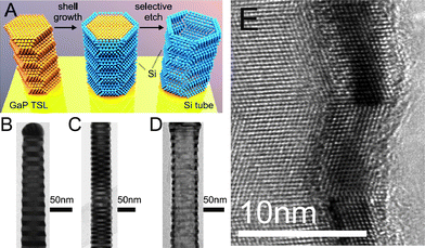 | ||
| Fig. 5 Illustrations of radial nanowire heterostructures. (a) Schematics of the crystal structure transfer from core to shell. The core is a GaP nanowire composed of twin segments with alternating orientation, a twinning superlattice (TSL). A Si shell is grown around the GaP core and after shell growth the core is selectively etched, resulting in a Si tube. (b, c, d) TEM images of (b) a TSL GaP nanowire, (c) a TSL GaP nanowire with a Si shell, and (d) a remaining Si shell after selective etch of core. (e) High-resolution TEM image of a Si shell after core removal. Reprinted with permission from ref. 64. Copyright 2011 American Chemical Society. | ||
There are of course cases where the shell thickness is not homogeneous. Kavanagh et al. have recently grown InAs/GaAs core shell nanowire heterostructures on (100) substrates with MBE.76 Since the nanowires grow in the {111}B direction, they are not vertical but inclined. This leads to nanowires with uneven shell thickness and the uneven strain distribution causes the nanowires to bend. In this study the authors carefully investigate the dislocation formation in these structures and relate it to carrier transport. The shadowing effects in the MBE that leads to uneven shell thicknesses has also been considered by other researchers.77
Growth of ternary shells is potentially not as straightforward as growth of binary or elementary shells. This is because there can be an effective chemical potential difference between different facets and the different species can have different diffusion lengths. These effects have been proposed to explain phase segregation in AlInP shells on GaAs nanowires,78,79 see Fig. 6. Strain can also lead to phase segregation, but photoluminescence investigations show that the overall composition of the AlxIn1-xP shells was close to x = 0.5 so they are essentially lattice matched to the GaAs cores. Thus, no indications of strain induced phase segregation were reported.
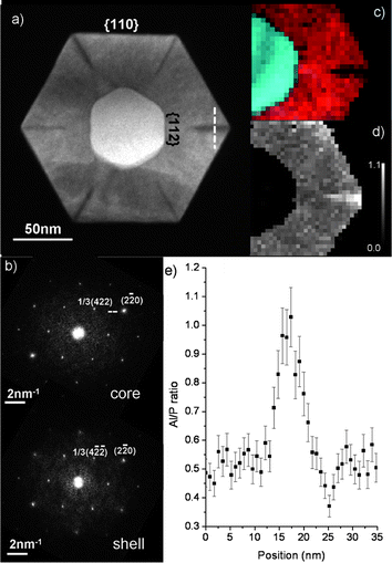 | ||
| Fig. 6 Phase segregation in an AlxIn1-xP ternary shell. (a) High angle annular dark field image of a cross section of a GaAs/AlxIn1-xP core/shell nanowire. (b) Fast Fourier transforms from the core and shell, respectively. (c) Electron energy loss spectrum imaging maps of In (red) and Ga (cyan). (d) Map of the Al/P ratio. Brighter contrast indicates higher Al/P ratio. (e) The Al/P ratio along the dashed white line in (a). The approximately 5 nm wide region in (e) where the Al/P ratio is close to one corresponds to the Al-rich domain. Reprinted with permission from ref. 79. Copyright 2010 Elsevier. | ||
Tambe et al. report growth of defect free GaAs/AlxGa1-xAs (x ≈ 0.9) radial heterostructures.80Energy dispersive X-ray spectroscopy shows that the AlGaAs shell is homogeneous in composition along the nanowire. Moreover, the authors find that the shell composition is mainly controlled by the deposition temperature. No phase segregation was reported for these shells. It has also been observed that the different growth mechanisms that lead to axial and radial growth (metal particle seeded growth and vapor phase growth respectively) can result in spontaneous formation of radial heterostructures when growing metal particle seeded nanowires in ternary materials.81,82Growth of AlGaAs nanowire structures thus results in radial heterostructures with a shell with higher Al content than the core.69,81,82 In addition, the shells formed due to unintentional radial overgrowth while growing InGaAs axial nanowire segments are most likely richer in indium than the core InGaAs segment.69Catalyst-free growth of InGaAs nanowires has resulted in a thin shell on which indium rich quantum dots have self-assembled.83 Dedicated growth of InAs self-assembled quantum dots, or Stranski-Krastanow islands, on the shells has been demonstrated in GaAs/AlAs core/shell nanowires.84
Several applications are being explored for radial nanowire heterostructures. Promising light emitting devices have been fabricated85–87 and they have been considered for applications in solar energy conversion.88–91 More exotic applications have also been explored; when Sköld et al. investigated the GaAs/AlInP core/shell structures the cores were selectively etched in order to characterize the shells separately by photoluminescence.78 The remaining solid shells, or hollow nanotubes, were later used in an ingenious process scheme to demonstrate electrophoretic transport of biomolecules.63 The same research group also has preliminary results of cell injection using hollow nanowires as syringes.
Hollow nanowires and radial nanowire heterostructures also seem to be very promising in thermoelectric applications. Significant reductions in the thermal conductivity for core/shell and tubular nanowires have been theoretically predicted,92,93 both as an effect of the increased surface-to-volume ratio that is gained by making them hollow94 and as an effect of a thin Ge shell covering a Si core nanowire.95 The promising theoretical predictions for hollow nanowires were one of the motivations for the hollow nanowires fabricated by Algra et al. discussed above and displayed in Fig. 5.64 For a recent overview of thermoelectric aspects of nanowire heterostructures and hollow nanowires, see ref. 96.
Summary and outlook
In this short highlight, we have given an overview of the current state-of-the-art of growth and understanding of epitaxial nanowire heterostructures. We have divided nanowire heterostructures into three categories: nanowire–substrate, axial, and radial heterostructures. Each of these categories has been given a dedicated section where we discuss problems and limitations, review experimental results, and highlight one or a few selected promising applications associated with that type of heterostructure.It is interesting to note that when it comes to pure growth aspects, such as interface control and the overall quality of the structures, the results reported in the seminal papers published 2002 from Berkley,24 Harvard,26,68 and Lund25 still represents state-of-the art. However, understanding of the growth has in many respects advanced considerably. Phenomenological models based on interface energetics explaining kinking in axial heterostructures have been developed. Models for strain accommodation in axial heterostructures and nanowire–substrate heterostructures have also been developed. Basic understanding of interface grading based on properties of the metal alloy particle in these kinds of heterostructures has also been reported.
As future research directions in nanowire heterostructure synthesis we see two promising areas: (i) usage of crystal structure tuning in combination with heterostructure growth in order to prevent kinking and facilitate straight growth and possibly also to optimize interface abruptness and (ii) advanced understanding of the properties of the metal seed particle so that the alloy can be tailored to enable abrupt interfaces and possibly also to enhance straight growth.
Better-controlled heterointerfaces will ensure the advancement of the research on quantum mechanical effects, such as tunneling through barriers and carrier confinement effects, in nanowires. The research on controlled synthesis and advanced characterization of nanowire heterostructures could in the long term lead to applications with a very positive impact on society. The most prominent applications can be found in electronics, optoelectronics, and energy harvesting. In the first two areas, III–V nanowire transistors, tunneling diodes, and light emitting diodes, all fabricated on silicon have been demonstrated. In the energy harvesting area, nanowire heterostructures are being considered as building blocks in both solar cell and thermoelectric applications. Only time will tell when or if these or other nanowire based applications will reach the market. In the meantime, we can tell for sure, a lot of valuable scientific knowledge is being generated.
Acknowledgements
This work was performed within the Nanometer Structure Consortium at Lund University (nmC@LU) and funded by the Swedish Research Council. We express our sincerest gratitude to T. Fukui, C. Jagadish, J. Zou, F. M. Ross, E. P. A. M. Bakkers, M. Hocevar, J. B. Wagner, and L. R. Wallenberg for sending us their figures and allowing us to reproduce them. We acknowledge J. Bolinsson, M. Borgström, and J. Wallentin for useful discussions.References
- K. W. Kolasinski, Curr. Opin. Solid State Mater. Sci., 2006, 10, 182 CrossRef CAS.
- N. Wang, Y. Cai and R. Q. Zhang, Mater. Sci. Eng., R, 2008, 60, 1 CrossRef.
- M. E. Messing, K. Hillerich, J. Bolinsson, K. Storm, J. Johansson, K. A. Dick and K. Deppert, Nano Res., 2010, 3, 506 CrossRef CAS.
- M. E. Messing, K. Hillerich, J. Johansson, K. Deppert and K. A. Dick, Gold Bull., 2009, 42, 172 CrossRef CAS.
- R. S. Wagner and W. C. Ellis, Appl. Phys. Lett., 1964, 4, 89 CrossRef CAS.
- B. A. Wacaser, K. A. Dick, J. Johansson, M. T. Borgström, K. Deppert and L. Samuelson, Adv. Mater., 2009, 21, 153 CrossRef CAS.
- J. W. Matthews and A. E. Blakeslee, J. Cryst. Growth, 1974, 27, 118 CAS.
- R. D. Bringans, Crit. Rev. Solid State Mat. Sci., 1992, 17, 353 CrossRef CAS.
- T. Mårtensson, C. P. T. Svensson, B. A. Wacaser, M. W. Larsson, W. Seifert, K. Deppert, A. Gustafsson, L. R. Wallenberg and L. Samuelson, Nano Lett., 2004, 4, 1987 CrossRef.
- K. L. Kavanagh, Semicond. Sci. Technol., 2010, 25, 024006 CrossRef.
- K. Tomioka, Y. Kobayashi, J. Motohisa, S. Hara and T. Fukui, Nanotechnology, 2009, 20, 145302 CrossRef.
- T. Tanaka, K. Tomioka, S. Hara, J. Motohisa, E. Sano and T. Fukui, Appl. Phys. Express, 2010, 3, 025003 CrossRef.
- T. Mårtensson, J. B. Wagner, E. Hilner, A. Mikkelsen, C. Thelander, J. Stangl, B. J. Ohlsson, A. Gustafsson, E. Lundgren, L. Samuelson and W. Seifert, Adv. Mater., 2007, 19, 1801 CrossRef.
- B. Mandl, J. Stangl, E. Hilner, A. A. Zakharov, K. Hillerich, A. W. Dey, L. Samuelson, G. Bauer, K. Deppert and A. Mikkelsen, Nano Lett., 2010, 10, 4443 CrossRef CAS.
- L. C. Chuang, M. Moewe, C. Chase, N. P. Kobayashi, C. Chang-Hasnain and S. Crankshaw, Appl. Phys. Lett., 2007, 90, 043115 CrossRef.
- G. E. Cirlin, V. G. Dubrovskii, I. P. Soshnikov, N. V. Sibirev, Y. B. Samsonenko, A. D. Bouravleuv, J. C. Harmand and F. Glas, Phys. Status Solidi RRL, 2009, 3, 112 CrossRef CAS.
- J. Shi and X. D. Wang, J. Phys. Chem. C, 2010, 114, 2082 CAS.
- F. Glas, Phys. Rev. B: Condens. Matter Mater. Phys., 2006, 74, 121302 CrossRef.
- C. Rehnstedt, T. Martensson, C. Thelander, L. Samuelson and L. E. Wernersson, IEEE Trans. Electron Devices, 2008, 55, 3037 CrossRef CAS.
- L. E. Wernersson, C. Thelander, E. Lind and L. Samuelson, Proc. IEEE, 2010, 98, 2047 CrossRef CAS.
- S. A. Dayeh, Semicond. Sci. Technol., 2010, 25, 024004 CrossRef.
- M. T. Björk, H. Schmid, C. D. Bessire, K. E. Moselund, H. Ghoneim, S. Karg, E. Lortscher and H. Riel, Appl. Phys. Lett., 2010, 97, 163501 CrossRef.
- K. Tomioka and T. Fukui, Appl. Phys. Lett., 2011, 98, 083114 CrossRef.
- Y. Y. Wu, R. Fan and P. D. Yang, Nano Lett., 2002, 2, 83 CrossRef CAS.
- M. T. Björk, B. J. Ohlsson, T. Sass, A. I. Persson, C. Thelander, M. H. Magnusson, K. Deppert, L. R. Wallenberg and L. Samuelson, Nano Lett., 2002, 2, 87 CrossRef.
- M. S. Gudiksen, L. J. Lauhon, J. Wang, D. C. Smith and C. M. Lieber, Nature, 2002, 415, 617 CrossRef CAS.
- M. W. Larsson, J. B. Wagner, M. Wallin, P. Håkansson, L. E. Fröberg, L. Samuelson and L. R. Wallenberg, Nanotechnology, 2007, 18, 015504 CrossRef.
- C. Thelander, T. Mårtensson, M. T. Björk, B. J. Ohlsson, M. W. Larsson, L. R. Wallenberg and L. Samuelson, Appl. Phys. Lett., 2003, 83, 2052 CrossRef CAS.
- M. T. Björk, B. J. Ohlsson, C. Thelander, A. I. Persson, K. Deppert, L. R. Wallenberg and L. Samuelson, Appl. Phys. Lett., 2002, 81, 4458 CrossRef.
- C. Thelander, H. A. Nilsson, L. E. Jensen and L. Samuelson, Nano Lett., 2005, 5, 635 CrossRef CAS.
- E. Ertekin, P. A. Greaney, D. C. Chrzan and T. D. Sands, J. Appl. Phys., 2005, 97, 114325 CrossRef.
- H. Ye, P. F. Lu, Z. Y. Yu, Y. X. Song, D. L. Wang and S. M. Wang, Nano Lett., 2009, 9, 1921 CrossRef CAS.
- P. Caroff, M. E. Messing, B. M. Borg, K. A. Dick, K. Deppert and L. E. Wernersson, Nanotechnology, 2009, 20, 495606 CrossRef.
- P. Madras, E. Dailey and J. Drucker, Nano Lett., 2009, 9, 3826 CrossRef CAS.
- K. W. Schwarz and J. Tersoff, Phys. Rev. Lett., 2009, 102, 206101 CrossRef CAS.
- K. W. Schwarz and J. Tersoff, Nano Lett., 2011, 11, 316 CrossRef CAS.
- K. A. Dick, S. Kodambaka, M. C. Reuter, K. Deppert, L. Samuelson, W. Seifert, L. R. Wallenberg and F. M. Ross, Nano Lett., 2007, 7, 1817 CrossRef CAS.
- M. Paladugu, J. Zou, Y. N. Guo, G. J. Auchterlonie, H. J. Joyce, Q. Gao, H. H. Tan, C. Jagadish and Y. Kim, Small, 2007, 3, 1873 CrossRef CAS.
- K. A. Dick, Prog. Cryst. Growth Charact. Mater., 2008, 54, 138 CrossRef CAS.
- J. Bauer, V. Gottschalch, H. Paetzelt and G. Wagner, J. Cryst. Growth, 2008, 310, 5106 CrossRef CAS.
- M. Tchernycheva, G. E. Cirlin, G. Patriarche, L. Travers, V. Zwiller, U. Perinetti and J. C. Harmand, Nano Lett., 2007, 7, 1500 CrossRef CAS.
- C. P. T. Svensson, W. Seifert, M. W. Larsson, L. R. Wallenberg, J. Stangl, G. Bauer and L. Samuelson, Nanotechnology, 2005, 16, 936 CrossRef CAS.
- N. D. Zakharov, P. Werner, G. Gerth, L. Schubert, L. Sokolov and U. Gösele, J. Cryst. Growth, 2006, 290, 6 CrossRef CAS.
- P. Krogstrup, J. Yamasaki, C. B. Sorensen, E. Johnson, J. B. Wagner, R. Pennington, M. Aagesen, N. Tanaka and J. Nygard, Nano Lett., 2009, 9, 3689 CrossRef CAS.
- N. Li, T. Y. Tan and U. Gösele, Appl. Phys. A: Mater. Sci. Process., 2008, 90, 591 CrossRef CAS.
- C. Y. Wen, M. C. Reuter, J. Bruley, J. Tersoff, S. Kodambaka, E. A. Stach and F. M. Ross, Science, 2009, 326, 1247 CrossRef CAS.
- D. E. Perea, N. Li, R. M. Dickerson, A. Misra and S. T. Picraux, Nano Lett., 2011, 11, 3117 CrossRef CAS.
- F. Glas, J. C. Harmand and G. Patriarche, Phys. Rev. Lett., 2010, 104, 135501 CrossRef.
- L. E. Fröberg, B. A. Wacaser, J. B. Wagner, S. Jeppesen, B. J. Ohlsson, K. Deppert and L. Samuelson, Nano Lett., 2008, 8, 3815 CrossRef.
- F. Jabeen, G. Patriarche, F. Glas and J.-C. Harmand, J. Cryst. Growth, 2011, 323, 293 CrossRef CAS.
- I. Regolin, D. Sudfeld, S. Luttjohann, V. Khorenko, W. Prost, J. Kastner, G. Dumpich, C. Meier, A. Lorke and F. J. Tegude, J. Cryst. Growth, 2007, 298, 607 CrossRef CAS.
- M. Paladugu, J. Zou, Y. N. Guo, X. Zhang, Y. Kim, H. J. Joyce, Q. Gao, H. H. Tan and C. Jagadish, Appl. Phys. Lett., 2008, 93, 101911 CrossRef.
- L. Ouattara, A. Mikkelsen, N. Sköld, J. Eriksson, T. Knaapen, E. Cavar, W. Seifert, L. Samuelson and E. Lundgren, Nano Lett., 2007, 7, 2859 CrossRef CAS.
- S. D. Carnevale, J. Yang, P. J. Phillips, M. J. Mills and R. C. Myers, Nano Lett., 2011, 11, 866 CrossRef CAS.
- M. T. Borgström, J. Wallentin, J. Trägårdh, P. Ramvall, M. Ek, L. R. Wallenberg, L. Samuelson and K. Deppert, Nano Res., 2010, 3, 264 CrossRef.
- B. M. Borg, M. Ek, K. A. Dick, B. Ganjipour, A. W. Dey, C. Thelander and L.-E. Wernersson, manuscript, 2011 Search PubMed.
- H. A. Nilsson, T. Duty, S. Abay, C. Wilson, J. B. Wagner, C. Thelander, P. Delsing and L. Samuelson, Nano Lett., 2008, 8, 872 CrossRef CAS.
- E. D. Minot, F. Kelkensberg, M. van Kouwen, J. A. van Dam, L. P. Kouwenhoven, V. Zwiller, M. T. Borgström, O. Wunnicke, M. A. Verheijen and E. P. A. M. Bakkers, Nano Lett., 2007, 7, 367 CrossRef CAS.
- H. Pettersson, J. Trägårdh, A. I. Persson, L. Landin, D. Hessman and L. Samuelson, Nano Lett., 2006, 6, 229 CrossRef CAS.
- A. Tribu, G. Sallen, T. Aichele, R. Andre, J. P. Poizat, C. Bougerol, S. Tatarenko and K. Kheng, Nano Lett., 2008, 8, 4326 CrossRef CAS.
- N. Sköld, M. E. Pistol, K. A. Dick, C. Pryor, J. B. Wagner, L. S. Karlsson and L. Samuelson, Phys. Rev. B: Condens. Matter Mater. Phys., 2009, 80, 041312 CrossRef.
- J. W. W. van Tilburg, R. E. Algra, W. G. G. Immink, M. Verheijen, E. P. A. M. Bakkers and L. P. Kouwenhoven, Semicond. Sci. Technol., 2010, 25, 024011 CrossRef.
- N. Sköld, W. Hällstrom, H. Persson, L. Montelius, M. Kanje, L. Samuelson, C. N. Prinz and J. O. Tegenfeldt, Nanotechnology, 2010, 21, 155301 CrossRef.
- R. E. Algra, M. Hocevar, M. A. Verheijen, I. Zardo, G. G. W. Immink, W. J. P. van Enckevort, G. Abstreiter, L. P. Kouwenhoven, E. Vlieg and E. P. A. M. Bakkers, Nano Lett., 2011, 11, 1690 CrossRef CAS.
- M. A. Verheijen, G. Immink, T. de Smet, M. T. Borgstrom and E. P. A. M. Bakkers, J. Am. Chem. Soc., 2006, 128, 1353 CrossRef CAS.
- L. J. Lauhon, M. S. Gudiksen and C. M. Lieber, Philos. Trans. R. Soc. London, Ser. A, 2004, 362, 1247 CrossRef CAS.
- N. Sköld, L. S. Karlsson, M. W. Larsson, M. E. Pistol, W. Seifert, J. Trägårdh and L. Samuelson, Nano Lett., 2005, 5, 1943 CrossRef.
- L. J. Lauhon, M. S. Gudiksen, C. L. Wang and C. M. Lieber, Nature, 2002, 420, 57 CrossRef CAS.
- J. Bolinsson, K. Mergenthaler, L. Samuelson and A. Gustafsson, J. Cryst. Growth, 2011, 315, 138 CrossRef CAS.
- M. Ben-Ishai and F. Patolsky, Adv. Mater., 2010, 22, 902 CrossRef CAS.
- Y. J. Zhao, J. T. Smith, J. Appenzeller and C. Yang, Nano Lett., 2011, 11, 1406 CrossRef CAS.
- J. Johansson, L. S. Karlsson, C. P. T. Svensson, T. Mårtensson, B. A. Wacaser, K. Deppert, L. Samuelson and W. Seifert, Nat. Mater., 2006, 5, 574 CrossRef CAS.
- R. E. Algra, M. A. Verheijen, M. T. Borgström, L. F. Feiner, G. Immink, W. J. P. van Enckevort, E. Vlieg and E. P. A. M. Bakkers, Nature, 2008, 456, 369 CrossRef CAS.
- P. Caroff, K. A. Dick, J. Johansson, M. E. Messing, K. Deppert and L. Samuelson, Nat. Nanotechnol., 2009, 4, 50 CrossRef CAS.
- K. A. Dick, P. Caroff, J. Bolinsson, M. E. Messing, J. Johansson, K. Deppert, L. R. Wallenberg and L. Samuelson, Semicond. Sci. Technol., 2010, 25, 024009 CrossRef.
- K. L. Kavanagh, J. Salfi, I. Savelyev, M. Blumin and H. E. Ruda, Appl. Phys. Lett., 2011, 98, 152103 CrossRef.
- M. Heigoldt, J. Arbiol, D. Spirkoska, J. M. Rebled, S. Conesa-Boj, G. Abstreiter, F. Peiro, J. R. Morante and A. F. I. Morral, J. Mater. Chem., 2009, 19, 840 RSC.
- N. Sköld, J. B. Wagner, G. Karlsson, T. Hernan, W. Seifert, M. E. Pistol and L. Samuelson, Nano Lett., 2006, 6, 2743 CrossRef.
- J. B. Wagner, N. Sköld, L. R. Wallenberg and L. Samuelson, J. Cryst. Growth, 2010, 312, 1755 CrossRef CAS.
- M. J. Tambe, S. K. Lim, M. J. Smith, L. F. Allard and S. Gradecak, Appl. Phys. Lett., 2008, 93, 151917 CrossRef.
- C. Chen, S. Shehata, C. Fradin, R. LaPierre, C. Couteau and G. Weihs, Nano Lett., 2007, 7, 2584 CrossRef CAS.
- S. K. Lim, M. J. Tambe, M. M. Brewster and S. Gradecak, Nano Lett., 2008, 8, 1386 CrossRef CAS.
- M. Heiss, B. Ketterer, E. Uccelli, J. R. Morante, J. Arbiol and A. F. I. Morral, Nanotechnology, 2011, 22, 195601 CrossRef.
- E. Uccelli, J. Arbiol, J. R. Morante and A. F. I. Morral, ACS Nano, 2010, 4, 5985 CrossRef CAS.
- C. P. T. Svensson, T. Mårtensson, J. Trägårdh, C. Larsson, M. Rask, D. Hessman, L. Samuelson and J. Ohlsson, Nanotechnology, 2008, 19, 305201 CrossRef.
- F. Qian, Y. Li, S. Gradecak, H. G. Park, Y. J. Dong, Y. Ding, Z. L. Wang and C. M. Lieber, Nat. Mater., 2008, 7, 701 CrossRef CAS.
- K. Tomioka, J. Motohisa, S. Hara, K. Hiruma and T. Fukui, Nano Lett., 2010, 10, 1639 CrossRef CAS.
- Y. Tak, S. J. Hong, J. S. Lee and K. Yong, J. Mater. Chem., 2009, 19, 5945 RSC.
- H. Goto, K. Nosaki, K. Tomioka, S. Hara, K. Hiruma, J. Motohisa and T. Fukui, Appl. Phys. Express, 2009, 2, 035004 CrossRef.
- Y. J. Dong, B. Z. Tian, T. J. Kempa and C. M. Lieber, Nano Lett., 2009, 9, 2183 CrossRef CAS.
- F. Boxberg, N. Söndergaard and H. Q. Xu, Nano Lett., 2010, 10, 1108 CrossRef CAS.
- R. G. Yang, G. Chen and M. S. Dresselhaus, Nano Lett., 2005, 5, 1111 CrossRef CAS.
- R. Prasher, Appl. Phys. Lett., 2006, 89, 063121 CrossRef.
- J. Chen, G. Zhang and B. W. Li, Nano Lett., 2010, 10, 3978 CrossRef CAS.
- M. Hu, K. P. Giapis, J. V. Goicochea, X. L. Zhang and D. Poulikakos, Nano Lett., 2011, 11, 618 CrossRef CAS.
- G. Q. Zhang, Q. X. Yu, W. Wang and X. G. Li, Adv. Mater., 2010, 22, 1959 CAS.
| This journal is © The Royal Society of Chemistry 2011 |