Crystal growth and characterization of RbTi1−x−yYbxNbyOPO4/RbTiOPO4 (001) non-linear optical epitaxial layers†
Jaume
Cugat
,
Rosa Maria
Solé
,
Joan J.
Carvajal
,
Maria Cinta
Pujol
,
Xavier
Mateos
,
Francesc
Díaz
and
Magdalena
Aguiló
*
Física i Cristal·lografia de Materials i Nanomaterials (FiCMA-FiCNA), Universitat Rovira i Virgili (URV), Campus Sescelades, C/Marcel·lí Domingo s/n E-43007, Tarragona, Spain. E-mail: magdalena.aguilo@urv.cat
First published on 4th January 2011
Abstract
In this paper we report the growth of RbTi1−x−yYbxNbyOPO4/RbTiOPO4 epitaxial layers by the liquid phase epitaxy method and discuss their structural and optical characterization. The layers were grown on (001) oriented substrates because this plane contains the phase-matching direction for Yb3+ type-II second-harmonic generation. In RbTi0.971Yb0.015Nb0.014OPO4/RbTiOPO4 epitaxial layers we obtained enough contrast of refractive indices (Δnz = 0.007 at 632.8 nm) to guide the light in TM polarization. The maximum Yb3+ concentration obtained in these layers was 1.43 × 10²⁰ atoms per cm3, which may be suitable for laser action. The lattice mismatch between the epitaxial layers and the substrates was low enough to obtain high quality epitaxial layers. Confinement of the light at 532 and 632.8 nm was demonstrated and there was good agreement between theoretical calculations, dark-mode spectra and modes of propagation.
1. Introduction
RbTiOPO4 (RTP) belongs to the KTiOPO4 (KTP) family of non-linear optical crystals. At room temperature, the crystal symmetry of RTP is orthorhombic and belongs to the non-centrosymmetric space group Pna21, with lattice parameters a = 12.974(2) Å, b = 6.494(3) Å and c = 10.564(6) Å.1RTP crystals are positive biaxial crystals, with nx < ny < nz (na < nb < nc) and point symmetry mm2. Because of their non-centrosymmetry and non-linearity, they can be used for frequency doubling of lasers that emit in the IR spectral range.2 In the non-linear optical process, the (001) plane is especially interesting because it contains the Yb3+ type-II phase-matching direction and the ferroelectric vector is parallel to the [001] direction. This enables domains that are useful for Quasi Phase Matching (QPM) processes to be obtained. Moreover, RTP can be doped with active ions to obtain self-frequency doubling (SFD) materials, which are useful for compact and efficient laser sources in the visible range. Moreover, all these properties can be converged in waveguides for integrated photonics. A waveguide structure to confine the interacting optical waves enables compact and efficient devices to be constructed.3 Thin-film optical waveguides also offer interesting possibilities for non-linear optics since the intrinsic confinement of the electromagnetic field in at least one dimension to distances of the order of the radiation wavelength leads to high power densities.4Ytterbium is interesting because of its emission at a wavelength of around 1 µm and its simple energy level scheme consisting of only two energy levels: the ground state 2F7/2 and the excited state 2F5/2. The Yb3+ ion has several advantages, including its broad absorption and emission bandwidth, low quantum defect and long lifetime. It also has no absorption losses at the second-harmonic generation (SHG) frequency, which makes it particularly relevant for SFD.5
In an earlier study we investigated the RE3+ doping of KTP.6 The RE3+ distribution coefficients obtained were very low (typically about 10−3). RTP has a higher Yb3+ distribution coefficient than KTP but it is still too low for laser operation. It has recently been shown that the distribution coefficient of Yb3+ in RTP can be increased by co-doping with Nb5+ (ref. 5) and lasing in RTP co-doped with Nb5+ and Yb3+ has been demonstrated.7 Growing Yb,Nb:RTP single crystals with high optical quality presents several difficulties, mainly associated with the low growth rate, the crystal morphology (plate shape) and the tendency for cracks to appear.8 To increase the optical absorption of Yb3+ in RTP by increasing the optical path, and guiding the light, we grew epitaxial composites of Yb:RTP/RTP (001) by the Liquid Phase Epitaxy (LPE) method. However, due to the low Yb3+ distribution coefficients in RTP, the refractive indices contrast between the epilayers and the substrate was too low for optical waveguiding. To increase the distribution coefficient of Yb3+ in RTP and increase the optical absorption in the crystals and the contrast of refractive indices for guiding the light, we grew Yb:Nb:RTP/RTP epitaxial films.
Here we describe the crystal growth characteristics of bulk crystals for substrates and report suitable conditions for obtaining Yb:RTP/RTP and Yb:Nb:RTP/RTP epitaxial layers. We characterize the epitaxial layers by measuring the refractive indices, ion concentration, lattice parameters, etc. Finally, we study the light-guiding properties at 632.8 and 532 nm.
2. Experimental section
2.1. Liquid-Phase Epitaxial (LPE) growth
Liquid-phase epitaxy experiments were carried out in a special vertical furnace built with better isolation and a larger tubular core than the furnace used for bulk single crystal growth. We obtained a wide zone of uniform temperature so that the temperature gradient in the solution was practically zero. The crucible used was cylindrical, 30 mm in diameter and 40 mm in height, and filled with about 80 g of solution. The reagents used were the same as in the growth of substrates (Rb2CO3 (99%), NH4H2PO4 (99%), TiO2 (99.9%) and WO3 (99.9%)), and Yb2O3 (99.9%) and Nb2O5 (99.9%) were used for substitution. To obtain a highly confined light waveguide, we used several solution compositions in order to obtain a suitable contrast of refractive indices. Mainly we used three different oxide relations between Rb2O–P2O5–(TiO2 + Nb2O5 + Yb2O3)–WO3. In experiments 1–8 in Table 2, we used solutions with composition Rb2O–P2O5–(TiO2 − Nb2O5 + Yb2O3)–WO3 = 40.80–27.20–32.00–0.00 (mol%) and different levels of substitution of TiO2 by Yb2O3 and Nb2O5, taking into account the results of varying the crystallization region of RTP by substituting TiO2 with Nb2O5 and Yb2O3.9 To reduce the viscosity of the growth solution, as in the solution used to obtain the substrates, we used WO3-containing solutions. In experiments 9 and 10, we used solutions with 10 mol% of WO3. In this case, we did a trade-off between the presence of W6+ in the layer and solution viscosity because incorporating W6+ into the crystals could hinder future applications. Taking into account the crystallization region of RTP in solutions containing 10 mol% WO3, we chose a solution composition located in the central zone of the RTP crystallization region. The composition used was Rb2O–P2O5–(TiO2 + Nb2O5 + Yb2O3)–WO3 = 43.90–23.6–22.50–10.00 (mol%). In experiment 11, we used a solution containing 20 mol% WO3, with composition Rb2O–P2O5–(TiO2 + Nb2O5 + Yb2O3)–WO3 = 43.82–22.58–13.60–20.00 (mol%), which has already been used by our group to successfully grow single crystals.10 After homogenization of the solution, its saturation temperature was accurately determined with a (001)-oriented RTP seed. We also studied the kinetics of the growth/dissolution processes because this is important in deciding the experimental conditions for growing the LPE single-crystal layers. In all experiments we used the same type of substrate, (001) plates with polished faces to grow layers along the (001) plane. The plate substrates were prepared by cutting 1.5 mm thick slices from single crystals with a diamond saw and polishing the slices with alumina powder. The (001) or a–b plane is interesting because it contains the type-II non-critical phase matching direction for the ytterbium laser emission wavelength range (from 985 to 1118 nm). The substrates were cut with the edges parallel to the a and b crystallographic directions. Before they were placed in the furnace, the substrates were carefully and consecutively cleaned in the following solutions: 1![[thin space (1/6-em)]](https://www.rsc.org/images/entities/char_2009.gif) :1 HNO3:H2O (in volume), distilled water, acetone and ethanol (5 minutes in each case). They were then slowly introduced into the furnace to prevent thermal stresses and held above the surface of the solution for about 1 h to achieve thermal equilibrium with the solution. The substrates were then dipped into the solution and kept at a temperature 1 K above the saturation temperature for 5 minutes to dissolve the outer part of the crystal. To begin epitaxial growth, the temperature of the solution was then decreased to 2–10 K below the saturation temperature and growth was allowed to progress for several hours.
:1 HNO3:H2O (in volume), distilled water, acetone and ethanol (5 minutes in each case). They were then slowly introduced into the furnace to prevent thermal stresses and held above the surface of the solution for about 1 h to achieve thermal equilibrium with the solution. The substrates were then dipped into the solution and kept at a temperature 1 K above the saturation temperature for 5 minutes to dissolve the outer part of the crystal. To begin epitaxial growth, the temperature of the solution was then decreased to 2–10 K below the saturation temperature and growth was allowed to progress for several hours.
Finally, the crystal was removed from the solution and kept a few millimetres above the surface of the solution while the furnace was cooled to room temperature at 15 K h−1 to avoid thermal stresses between the substrate and the epitaxial layer that could lead to cracks. The epitaxial layers were observed using an optical microscope, a Sensofar PLµ 2300 interferometric microscope, and finally an atomic force microscope (AFM). With these devices we observed the morphologies of the epitaxial layers. We also profiled the layers, obtaining the thickness along several directions of the epitaxial layer.
To study how the thickness of the layer changes as a function of the growth time (velocity of growth), in experiment 3 the substrate was initially dipped 10 mm into the solution and then pulled out in steps of 2 mm for known time intervals. In the final step, the substrate was completely removed from the solution.
The chemical composition of the RbTi1−x−yYbxNbyOPO4 single crystals and that of the epitaxial layers obtained by LPE were determined by electron probe microanalysis (EPMA) in a Cameca SX-50 microprobe analyzer. The electron beam was generated with an intensity of 15 nA and an accelerating voltage of 20 KV. The X-rays produced by the samples were detected and characterized by a wavelength-dispersive spectrometer (WDS). The X-ray pattern of the sample was compared with that of standard samples containing known concentrations of the elements to be analyzed. RbTiOPO4 was used as a standard for determining Rb, Ti and P. Nb metal was used to determine the Nb concentration and YbF3 was used for Yb measurements. All samples were prepared in the same way: first, a small piece of crystal was placed in a cylindrical container, where a polyester resin was added with a catalyst. After the resin had solidified, the surface containing the crystal was polished with a 1 µm diamond powder.
2.2. X-Ray powder diffraction
To measure the unit cell parameters, small single crystals of Yb:Nb:RTP were grown on a Pt wire immersed in the solution. The saturation temperature was determined by decreasing the solution temperature at intervals of 10 K every 30 minutes until the crystals appeared. The temperature of the solution was then maintained for several hours to grow the crystals. The lattice parameters of these crystals with different compositions were determined at room temperature by X-ray powder diffraction (XRD). The data were collected with a Siemens D5000 X-ray powder diffractometer with the Bragg–Brentano parafocusing geometry and a θ–θ configuration. Cu Kα radiation was used in these experiments and the 2θ range was from 10 to 70°, with a step scan (ss) of 0.02° and a scan time (st) of 16 s. The crystal cell parameters were calculated from the diffraction data using the FULLPROF program11 and the Rietveld method.12 These results were used to calculate the lattice mismatch between the epitaxial layer and the substrate, which is of great interest for optimizing the quality of the epilayer/substrate interface.2.3. Planar waveguide fabrication and characterization techniques
We used the epitaxies grown in the previous steps to fabricate planar waveguides. The first step in the fabrication was to remove the epilayer grown on one of the faces of the substrate. The remaining epilayer was then polished with alumina powder to obtain a 50 µm thick highly transparent layer to be used for measuring the refractive indices. We were then able to calculate the number of propagation modes as a function of the thickness of the epitaxy. After polishing the sample, we measured the refractive indices of the epitaxy and substrate using the total internal-reflecting-angle law, coupling the light by a prism using a Metricon prism coupler.Visualization of the propagation modes in the epitaxial layer requires calculation of the proper thickness to obtain a small number of modes. Using the refractive indices, we applied the equation of dispersion for a wave propagating along the guide:13

, where j = a, s and


We were then able to determine the number of allowed modes for a given thickness of the epitaxial layer.
After checking the calculations, the samples were polished until the thickness required to obtain a few propagation modes. The prism coupler system was used to record the dark-mode spectrum at 632.8 nm using a He–Ne laser beam as the light source with TM polarization. The same experiments were carried out using a 532 nm laser beam to record the dark-mode spectrum with TM polarization. Finally, we used a CCD camera to visualize the different guided modes that the waveguide can support by coupling the light of the He–Ne laser emitting at 632.8 nm and the frequency doubled Nd:YAG laser emitting at 532 nm at the input and output ends of the waveguide with microscope objectives (40× and 60×, respectively).
3. Results and discussion
3.1. Single-crystal growth for substrates and liquid phase epitaxial (LPE) growth
RTP crystals, to be cut for substrates, were grown in a tubular furnace as described in the Experimental section. Table 1 shows the crystal growth conditions, dimensions and weights of several single crystals that were cut for substrates. The crystals obtained were generally colorless, transparent and free of inclusions and cracks. Their dimensions were 14.0–9.2, 15.1–26.0 and 11.1–21.9 mm in the a, b and c crystallographic directions, respectively, and their weights ranged from 5.71 g to 13.94 g. In several experiments we pulled the crystals (see Table 1) to obtain a larger dimension along the c crystallographic direction in the single crystals. From each single crystal we were therefore able to cut more substrates. Moreover, as observed in Table 1, by pulling the crystal, the average growth velocity increases. The crystals were then cut in plates of dimensions 4.2–10.3, 12–19.3 and 1 mm along the a, b and c crystallographic directions, respectively, to be used for substrates. All the substrates were cut perpendicular to the c crystallographic direction or (001) face to obtain the a–b plane. This plane is interesting because it contains the non-critical phase matching (PM) type-II SHG direction. Moreover, the a–b plane is perpendicular to the ferroelectric vectors of the domains, which makes it possible to produce a periodic inversion of them and realize Quasi Phase Matching. The plates were polished to optical quality to obtain surfaces with 50–80 nm of roughness and 8–20 m of curvature, otherwise the defects could propagate from the interface to the epitaxial film. Fig. 1 shows a photograph of an as-grown crystal to be cut for substrates. Table 1 summarizes the dimensions and weights of some of the crystals grown for this purpose.| Experiment number | Cooling interval/K | Total pulling/mm | Crystal dimensions a × b × c/mm | Crystal weight/g |
|---|---|---|---|---|
| 1 | 20 | 0 | 14.0 × 26.0 × 11.1 | 7.99 |
| 2 | 20 | 0 | 14.9 × 15.1 × 15.9 | 5.71 |
| 3 | 27 | 4 | 17.3 × 18.7 × 20.4 | 9.37 |
| 4 | 28 | 5.5 | 17.9 × 20.0 × 21.5 | 12.32 |
| 5 | 30 | 6.5 | 19.2 × 21.1 × 21.9 | 13.94 |
 | ||
| Fig. 1 Photograph of an as-grown single crystal, to be cut for substrates. | ||
The epitaxial layers were grown by liquid phase epitaxy (LPE) from self-flux solutions and WO3-containing solutions. This method was successfully used earlier in the KTP family.14Table 2 summarizes the LPE experiments conducted using (001) substrate plates. We grew epitaxial layers as large as 16 mm, which, unlike with bulk crystals, have a very large optical path. The solution composition, substrate dimensions, ΔT = Ts − Tg (where Ts is the saturation temperature and Tg is the growth temperature) and growth time are shown in Table 2. Generally, the epitaxial layers were grown with high crystalline quality. The epitaxial layers grown in experiments 1–3 (see Table 2) have low concentrations of Yb3+ and, therefore, low contrasts of refractive indices, which make the guided modes of the light extremely difficult. Therefore, we grew RTP epitaxial layers doped with Yb3+ and Nb5+ (see experiments 4–11), bearing in mind that Nb5+ improves the distribution coefficient of Yb3+ and increases the contrast of the refractive indices. These composites, as we will see in the Waveguide characterization section, guided the light in TM polarization. Moreover, we grew epitaxial layers from WO3-containing solutions because the solutions containing W6+ are less viscous than self-flux solutions and allow for easier growth. Moreover, the poor incorporation of W6+ in the crystal structure is in competition with Nb5+, which helps to produce better charge compensation. Finally, the incorporation of W6+ into the crystal structure slightly increases the refractive index contrast along the c crystallographic direction, which allows for better confinement in TM polarization. Experiments 9–11 were done in WO3-containing solutions. Fig. 2(a) shows the as-grown epitaxial layer obtained in experiment 11 (see Table 2) and Fig. 2(b) shows the epilayer grown in experiment 9 (see Table 2) after it was polished down to a thickness of 10 µm.
| Experiment number | Solution composition Rb2O–P2O5–TiO2–Yb2O3–Nb2O5–WO3/mol% | Substrate dimensions a × b × c/mm | ΔT = Ts − Tg/K | Growth time/h |
|---|---|---|---|---|
| 1 | 40.8–27.2–30.08–1.92–0–0 | 6.7 × 16.9 × 1.0 | 2 | 3 |
| 2 | 40.8–27.2–30.08–1.92–0–0 | 6.5 × 12.0 × 1.0 | 2 | 6 |
| 3 | 40.8–27.2–30.08–1.92–0–0 | 6.9 × 19.3 × 1.0 | 2 | 0.30–1–2.30–4–15 |
| 4 | 40.8–27.2–30.4–0.64–0.96–0 | 4.2 × 18.5 × 1.0 | 2 | 16 |
| 5 | 40.8–27.2–29.76–1.92–0.32–0 | 6.5 × 18.5 × 1.0 | 2 | 5 |
| 6 | 40.8–27.2–29.76–1.92–0.32–0 | 9.6 × 13.6 × 1.0 | 2 | 5 |
| 7 | 40.8–27.2–29.44–1.92–0.64–0 | 10.3 × 18.2 × 1.0 | 2 | 6 |
| 8 | 40.8–27.2–29.44–1.92–0.64–0 | 6.2 × 16.1 × 1.0 | 2 | 6 |
| 9 | 43.9–23.6–20.70–1.35–0.45–10 | 10.24 × 18.14 × 1.0 | 9 | 7 |
| 10 | 43.9–23.6–20.70–1.35–0.45–10 | 10.15 × 12.58 × 1.0 | 10 | 6 |
| 11 | 43.82–22.58–12.92–0.27–0.41–20 | 8.6 × 16.2 × 1.0 | 7 | 3 |
 | ||
| Fig. 2 (a) Photograph of the as-grown epitaxy obtained in experiment 11 (Table 2). (b) Photograph of the epitaxy grown in experiment 9 (Table 2) after a polishing process. | ||
The morphologies of the as-grown epitaxial layers were observed by optical microscope, confocal microscope and atomic force microscope, depending on the scale of observation. The surfaces of the epilayers grown from self-flux solutions were generally smoother than those of the epilayers grown from WO3-containing solutions. Fig. 3 shows a confocal image of the epilayer grown in experiment 9, and a detail of a 100 × 100 µm2 region obtained by AFM. There is also a profile of the 75–125 nm high macrosteps generated by screw dislocations. The reason why morphologies such as screw dislocations and macrosteps were obtained at the surface of the epilayers grown from WO3-containing solutions while the epilayers grown from self-flux solutions were generally smoother could be the lower viscosity of the WO3-containing solutions, which permits a higher rate of growth.
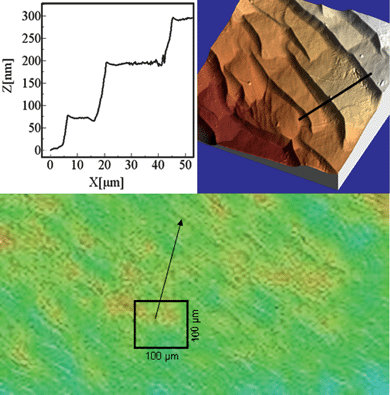 | ||
| Fig. 3 Confocal image of the epilayer grown in experiment 9. Detail of a 100 × 100 µm2 region obtained by AFM and profile of the macrosteps observed in the AFM image. | ||
In experiment 3, we studied the dependence of layer thickness on growth time by keeping all the other growth conditions constant. As we explained in the Experimental section, the substrate was initially dipped 10 mm into the solution and pulled out in 2 mm steps at the time intervals given in Table 2. The thickness of the epitaxial layer grown on the different parts of the substrate (corresponding to different growth times) was measured with the confocal microscope. Similar measurements were taken at both sides of the central region of the crystal to check there was no important dispersion between the growth thicknesses of different crystal zones for the same growth time. The results are shown in Fig. 4, the inset of which shows the location of the three profiles along which the measurements were taken. Here a linear behavior is observed between the epitaxial thickness and the growth time, at least up to 5 hours of growth, with a slope of 8.3 µm h−1.
 | ||
| Fig. 4 Thickness of the epitaxial layer against the time of growth. The inset shows the location on the crystal of the three profiles used to take the measurements. | ||
The composition of the epitaxial layers was measured by EPMA (see Table 3). From these results we calculated the coefficients of distribution of Yb3+ and Nb5+, according to  for Yb3+ and
 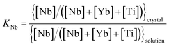 for Nb5+, where [Yb], [Nb] and [Ti] are the Yb3+, Nb5+ and Ti4+ concentrations in at%. W6+ concentration is not included in the chemical formula of the epitaxial layers in Table 3 because its distribution coefficient for substituting Ti in RTP is very low (in the order of 0.002).15
| Exp. num. |
|
|
Epilayer stoichiometry | K Yb | K Nb |
|---|---|---|---|---|---|
| 1 | 6 | 0 | RbTi0.995Yb0.005OPO4 | 0.04 | — |
| 6 | 6 | 1 | RbTi0.975Yb0.014Nb0.011OPO4 | 0.125 | 0.590 |
| 8 | 6 | 2 | RbTi0.971Yb0.015Nb0.014OPO4 | 0.135 | 0.378 |
| 9 | 6 | 2 | RbTi0.958Yb0.016Nb0.026OPO4 | 0.140 | 0.658 |
| 11 | 2 | 3 | RbTi0.983Yb0.004Nb0.013OPO4 | 0.106 | 0.226 |


Table 3 shows the composition of the epitaxial layers grown from different solution compositions and the Yb3+ and Nb5+ distribution coefficients. We can see that in the epitaxial layers grown in experiments 6, 8 and 9 (the numbers of the experiments are the same as those in Table 2), the Yb3+ concentration is of the same order, around 1020 atoms per cm3 which may be enough for laser demonstration.5 On the other hand, the epilayers grown in experiments 1 and 11 contain Yb3+ concentrations of the order of 1019 atoms per cm3. This concentration of active ions may not be enough for efficient lasing, though this would need to be checked. The lower Yb3+ concentration in sample 1 is due to the absence of Nb5+ in the solution since it has already been shown that the presence of Nb5+ in the solution helps to increase the Yb3+ distribution coefficient in the crystal.7 Moreover, the epilayer obtained in experiment 11 has a lower Yb3+ concentration than other epitaxial layers because in the solution the presence of Yb2O3 is much lower (approximately three times). From experiments 1, 6 and 8 we can see that the presence of Nb5+ increases the distribution coefficient of Yb3+. In experiment 9, there is an increase of KNb and also, though to a lesser extent, of KYb, perhaps because of the change in the solution composition.
The composition homogeneity of the epitaxial layers was analyzed by EPMA on the polished epilayer grown in experiment 8. Results show a homogeneity of Yb3+ and Nb5+ distribution along the epitaxy (see Fig. 5, which plots the concentration of the doping ions (Yb3+ + Nb5+) against the distance to the epitaxial surface). In this figure we can also see the sharp compositional change in the interface, which indicates that there is practically no diffusion of the doping ions from the layer to the substrate. This is interesting for the light confinement in the waveguides.
 | ||
| Fig. 5 Concentration of the doping ions (Yb3+ + Nb5+) against distance to the epitaxial surface. | ||
3.2. X-Ray powder diffraction
Table 4 gives the unit cell parameters of RTP and Yb:Nb:RTP obtained from the X-ray powder diffraction data discussed in the Experimental section. We can see that the presence of Yb3+ and Nb5+ in the crystal structure leads to an increase in the lattice parameters. An explanation for the expansion of the unit cell is that Nb5+ and Yb3+ have larger ionic radii than Ti4+, which causes the crystal unit cell to expand.16| Exp. num. | Stoichiometric formula | a/Å | b/Å | c/Å |
|---|---|---|---|---|
| Subs. | RbTiOPO4 | 12.9650(5) | 6.5007(3) | 10.5576(4) |
| 1 | RbTi0.995Yb0.005OPO4 | 12.9664(6) | 6.5012(3) | 10.5611(5) |
| 6 | RbTi0.975Yb0.014Nb0.011OPO4 | 12.9831(8) | 6.5116(4) | 10.5711(6) |
| 8 | RbTi0.971Yb0.015Nb0.014OPO4 | 12.9933(2) | 6.5150(6) | 10.5852(8) |
The lattice mismatch between the layer and the substrate is important for the quality of the layer/substrate interface. High mismatches produce stress at the interface, which favors the formation of cracks that can propagate through the layer.17 Taking into account the difference in the unit cell parameters between RbTi1−x−yYbxNbyOPO4 and RbTiOPO4 for different levels of substitution of Ti4+ by Yb3+ and Nb5+, we calculate the lattice mismatch from the expression
| f(hkl) = 100(S(hkl) (layer) − S(hkl) (substrate))/S(hkl) (substrate), |
| Epitaxial layer | Substrate/epilayer lattice mismatch (001) |
|---|---|
| RbTi0.995Yb0.005OPO4 | 0.05 |
| RbTi0.975Yb0.014Nb0.011OPO4 | 0.342 |
| RbTi0.971Yb0.015Nb0.014OPO4 | 0.473 |
3.3. Waveguide characterization
The epitaxial composites were characterized following the steps outlined in the Experimental section. The thin films were polished to a thickness of around 50 µm in order to ensure that the modes were not lost and the refractive indices could be determined. From the refractive indices we calculated the proper thickness for supporting a few propagation modes. The refractive indices of several layers and substrates measured with the Metricon prism coupler equipment are shown in Table 6 (note that we use the same experiment numbers as in Tables 2–4). We can see that in the epitaxial layers that contain neither Nb5+ nor W6+ substitution produces a negative contrast of refractive indices between the layer and the substrate (nlayer − nsubstrate). This means that the epitaxial layer cannot guide the light and we can conclude that Yb3+ substitution in RTP decreases the refractive indices. The results in Table 6 show that nz is the index most affected by the presence of Nb5+: it increases when Nb5+ increases. On the other hand, ny increases very slowly as Nb5+ increases. Finally, nx decreases in all cases when Nb5+ is incorporated into the crystal. These results show that the epitaxial layers are only able to guide the light in the TM polarization, which implies that the electric field vector is parallel to the c crystallographic direction. This is an important step for obtaining quasi-phase-matched periodically poled waveguides.| Exp. num. | Sample | Composition | n x | n y | n z |
|---|---|---|---|---|---|
| 4 | Layer | RbTi0.995Yb0.005OPO4 | 1.7864 | 1.7981 | 1.8863 |
| Substrate | RbTiOPO4 | 1.7892 | 1.8010 | 1.8882 | |
| 6 | Layer | RbTi0.975Yb0.014Nb0.011OPO4 | 1.7886 | 1.8019 | 1.8935 |
| Substrate | RbTiOPO4 | 1.7894 | 1.8013 | 1.8889 | |
| 8 | Layer | RbTi0.971Yb0.015Nb0.014OPO4 | 1.7872 | 1.8018 | 1.8956 |
| Substrate | RbTiOPO4 | 1.7895 | 1.8015 | 1.8898 | |
| 9 | Layer | RbTi0.958Yb0.016Nb0.026OPO4 | 1.7863 | 1.8016 | 1.8967 |
| Substrate | RbTiOPO4 | 1.7893 | 1.8015 | 1.8897 | |
| 11 | Layer | RbTi0.983Yb0.004Nb0.013OPO4 | 1.7885 | 1.8016 | 1.8944 |
| Substrate | RbTiOPO4 | 1.7894 | 1.8013 | 1.8884 | |
To demonstrate the light guiding in the epitaxial layers, we calculated the thickness needed to support a few propagation modes. Calculations were made using the expressions in the Experimental section and agreement between the theory and the experimental results using our waveguides was studied. To do so, we polished the epilayers obtained in experiments 8 and 9 until they reached a thickness of 10 and 5 µm, respectively. On the left hand side of Fig. 6(a) and (b) are the results of the thickness calculations against the effective refractive index. On the right hand side of this figure is the dark-mode spectrum done with the Metricon prism coupler equipment, in which the sharp grooves are due to the propagating modes of the light. In Fig. 6(a) for experiment 8, we can see 3 propagation modes at 532 nm and 2 propagation modes at 632.8 nm. This is logical because the confinement of the light is higher for low wavelengths. Fig. 6(b), on the other hand, which corresponds to the epilayer obtained in experiment 9, shows 7 propagation modes at 532 nm and 6 propagation modes at 632.8 nm. Note the high degree of agreement between the theoretical and the experimental results.
 | ||
| Fig. 6 Number of propagation modes versus the epitaxial thickness (left hand side) and dark-mode spectrum (right hand side). Calculations and experiments were done first at 532 nm and finally at 632.8 nm. (a) Sample 8, with 5 µm of thickness. (b) Sample 9, with 10 µm of thickness. | ||
Fig. 7(a) shows the guided modes of order m = 0, 1 and 2 propagated along the epitaxial layer grown in experiment 8 and polished to a 10 µm thickness. These modes were obtained using 532 nm light. These results agree well with the theoretical calculations (left hand side of Fig. 6(a)) and the dark mode spectrum for the same sample (right hand side of Fig. 6(a)). Fig. 7(b) shows the guided modes of order m = 0, 1, 2, 3 and 4 propagated along the epilayer grown in experiment 9 and polished to a thickness of 5 µm. In this case the wavelength of the light was 632.8 nm. Excitation of the guided mode of order 5 had some difficulties caused by the limitation of the movement steps of the support of the sample. We therefore tried to excite this mode of propagation and began to excite the mode of order 4. The lesser difference in the refractive indices along the c crystallographic direction between the epilayer and the substrate than between the epilayer and the air causes a shift in the energy density profile in the epitaxy–substrate interface due to the lower confinement of light than on the epitaxy–air boundary. This phenomenon can be seen in the propagation mode of order 0 in Fig. 7(b). These results confirmed experimentally that the waveguides obtained in this study confine the light successfully and that there is good agreement between the theoretical calculations (left hand side of Fig. 6(b)), the dark mode spectrum (right hand side of Fig. 6(b)) and our experimental results.
 | ||
| Fig. 7 CCD pictures of: (a) propagation modes of the order of m = 0, 1 and 2 in sample 8, with 5 µm of thickness at 532 nm. (b) Propagation modes of the order of m = 0, 1, 2, 3 and 4 in sample 9, with 10 µm of thickness at 632.8 nm. | ||
4. Conclusions
We have reported the growth of RbTi1−x−yYbxNbyOPO4/RbTiOPO4 (001) epitaxial layers and the efficient guiding possibilities. We achieved a maximum concentration of Yb3+ in the epilayers of 1.43 × 10²⁰ atoms per cm3. The maximum distribution coefficient of Nb5+ was 0.658. This allows a contrast of refractive indices between the epitaxial layer and the substrate that is high enough for optical waveguiding in TM polarization and to maintain an optimum Yb3+ concentration. After calculating the thickness of the epilayer needed to guide a few propagation modes, we showed that 532 and 632.8 nm light can be efficiently guided along these epitaxial layers. Photographs of several propagation modes are shown. In conclusion, these novel Yb:Nb:RTP/RTP (001) epitaxial composites are promising materials for integrated photonics and laser applications such as self-frequency doubling (SFD) waveguides and second-harmonic generation (SHG) waveguide lasers.Acknowledgements
This work was supported by the Spanish Government under projects MAT2008-06729-C02-02/NAN, MAT2008-04046-E/MAT, TEC2010-21574-C02-02, PI09/90527, HF2008-0045, DE2009-0002 and by the Catalan Authority under project 2009SGR235. J. Cugat thanks the Spanish Government for the FPI fellowship BES-2009-024190. J. J. Carvajal is supported by the Spanish Ministry of Education and Science and the European Social Fund under the Ramon y Cajal programs RYC2006-858.References
- P. A. Thomas, S. C. Mayo and B. E. Watts, Acta Crystallogr., Sect. B: Struct. Sci., 1992, 48, 401 CrossRef.
- C. Zumsteg, C. J. Bierlein and T. E. Gier, J. Appl. Phys., 1976, 47, 4980 CrossRef CAS.
- S. Suhara and M. Fujimura, Waveguides and Nonlinear-Optic Devices, Springer, Photonics, 2003 Search PubMed.
- G. I. Stegeman and C. T. Seaton, J. Appl. Phys., 1985, 58, R57 CrossRef CAS.
- X. Mateos, V. Petrov, A. Peña, J. J. Carvajal, M. Aguiló, F. Díaz, P. Segonds and B. Boulanger, Opt. Lett., 2007, 32, 1929 Search PubMed.
- (a) R. Solé, V. Nikolov, I. Koseva, P. Peshev, X. Ruiz, C. Zaldo, M. J. Martín, M. Aguiló and F. Díaz, Chem. Mater., 1997, 9, 2745 CrossRef CAS; (b) C. Zaldo, M. Rico, F. Díaz and J. J. Carvajal, Opt. Mater. (Amsterdam), 1999, 13, 175 Search PubMed.
- J. J. Carvajal, R. Solé, Jna. Gavaldà, J. Massons, P. Segonds, B. Boulanger, A. Brenier, G. Boulon, J. Zaccaro, M. Aguiló and F. Díaz, Opt. Mater. (Amsterdam), 2004, 26, 313 Search PubMed.
- J. J. Carvajal, R. Solé, Jna. Gavaldà, J. Massons, M. Aguiló and F. Díaz, Cryst. Growth Des., 2001, 1(6), 479 CrossRef CAS.
- J. J. Carvajal, V. Nikolov, R. Solé, Jna. Gavaldà, J. Massons, M. Aguiló and F. Díaz, Chem. Mater., 2002, 14, 3136 CrossRef CAS.
- A. Peña, J. J. Carvajal, M. C. Pujol, X. Mateos, M. Aguiló, F. Díaz, V. Petrov, P. Segonds and B. Boulanger, Opt. Express, 2007, 15, 14580 CrossRef CAS.
- J. Rodriguez-Carvajal, Short Reference Guide of the Program FULLPROF, Laboratoire Leon Brilloin, 1998 Search PubMed.
- R. A. Young, The Rietveld Method, Oxford Science Publication, International Union of Crystallography, 1995 Search PubMed.
- (a) P. K. Tien, R. Ulrich and R. J. Martin, Appl. Phys. Lett., 1969, 14, 291 CrossRef; (b) A. Boudrioua, P. Moretti, J. C. Loulergue and K. Polgar, Opt. Mater. (Amsterdam), 2000, 14, 31 Search PubMed.
- (a) C. Dubs, J. P. Ruske, E. Werner, A. Tünnermann, Ch. Schimidt and G. Bruchlos, Opt. Mater. (Amsterdam), 2001, 17, 477 Search PubMed; (b) R. Solé, V. Nikolov, A. Vilalta, J. J. Carvajal, J. Massons, Jna. Gavaldà, M. Aguiló and F. Díaz, J. Mater. Res., 2002, 17(3), 563 CrossRef CAS.
- R. Solé, V. Nikolov, I. Koseva, P. Peshev, X. Ruiz, C. Zaldo, M. J. Martín, M. Aguiló and F. Díaz, Chem. Mater., 1997, 9, 2745 CrossRef CAS.
- R. D. Shannon, Acta Crystallogr., Sect. A: Cryst. Phys., Diffr., Theor. Gen. Crystallogr., 1976, 32, 751 CrossRef.
- R. Solé, V. Nikolov, A. Vilalta, J. J. Carvajal, J. Massons, Jna. Gavaldà, M. Aguiló and F. Díaz, J. Cryst. Growth, 2002, 237, 602 CrossRef.
- A. Aznar, O. Silvestre, M. C. Pujol, R. Solé, M. Aguiló and F. Díaz, Cryst. Growth Des., 2006, 6, 1781 CrossRef CAS.
Footnote |
| † Electronic supplementary information (ESI) available: Experimental details of single crystal growth for substrates. See DOI: 10.1039/c0ce00647e |
| This journal is © The Royal Society of Chemistry 2011 |