Stamps, inks and substrates: polymers in microcontact printing
Tobias
Kaufmann
and
Bart Jan
Ravoo
*
Organic Chemistry Institute, Westfälische Wilhelms-Universität Münster, Corrensstrasse 40, 48149, Münster, Germany. E-mail: b.j.ravoo@uni-muenster.de
First published on 11th January 2010
Abstract
Microcontact printing (μCP) is a straightforward method for the preparation of micro- and nanostructured surfaces. The key element in μCP is a polymeric stamp with a relief pattern. This stamp is “inked” and put in contact with the substrate surface. Ideally, the ink is transferred from stamp to substrate only in the area of contact. This review focuses on the important role of polymers in μCP. First of all, polymers are the material of choice to make μCP stamps. Furthermore, μCP is a useful method for preparing microstructured polymer surfaces. Polymers can be applied as inks in μCP so that microstructured polymer surfaces are obtained in a single printing step. Microstructured polymer surfaces can also be obtained by μCP on polymer substrates. A wide range of inks – including polymer inks – can be patterned on polymer substrates by μCP. In short, polymers are widely used as stamps, inks and substrates in μCP and we have organized this review accordingly.
 Tobias Kaufmann | Tobias Kaufmann (born in 1982 in Neuss, Germany) studied chemistry at the Westfälische Wilhelms-Universität Münster from 2003 to 2008. He graduated with a diploma thesis entitled “Aminolysis by microcontact chemistry”. The topic of his PhD thesis is microcontact chemistry on flexible surfaces. |
 Bart Jan Ravoo | Bart Jan Ravoo (1970) studied chemistry in Groningen (The Netherlands). He held a postdoctoral scholarship at University College Dublin and an assistant professorship at the University of Twente (The Netherlands). Since 2007 he is professor at the Westfälische Wilhelms-Universität Münster (Germany). His research focuses on biomimetic supramolecular chemistry and surface functionalization by molecular self-assembly. |
1. Introduction
Microcontact printing (μCP) is a sophisticated version of a simple stamping process that is familiar even to most children. Similar to conventional printing, μCP also involves an ink, a substrate and a stamp. In contrast to the dyes that are normally used for printing, inks for μCP are printed in monomolecular layers. Instead of paper, clothing, or wood, the surfaces for μCP are usually ultra-flat metal, silicon or glass substrates. And – maybe the most remarkable difference – instead of macroscopic patterns, the stamps for μCP have microscale or even nanoscale structures. In less than two decades, μCP has emerged as a straightforward and cheap bench-top method for the preparation of micro- and nanostructured surfaces.It could be argued that the key element in μCP is a polymeric stamp, i.e. a slab of polymer that bears a microscale relief pattern on one side. This stamp is “inked” and put in contact with the substrate surface. Ideally, the ink is transferred from stamp to substrate only in the area of contact. The process of μCP is schematically depicted in Fig. 1.
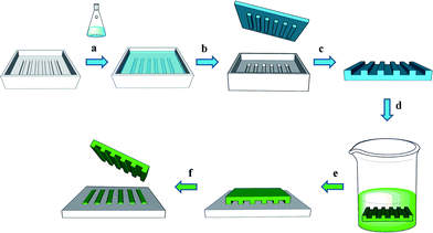 | ||
| Fig. 1 Key steps in microcontact printing (μCP): (a) a prepolymer is poured on a photolithographically structured master, (b) the prepolymer is cured and the elastomer stamp is peeled off the master, (c) the stamp is cut in smaller pieces, (d) the stamp is inked by soaking it in an ink solution, (e) the ink is printed by contacting an inked stamp with a suitable surface, (f) a patterned substrate is obtained. Alternatively to (a) and (b), a stamp can also be obtained by hot embossing. Alternatively to (c), wafer-size stamps can also be used. Alternatively to (d), a stamp can be inked by spreading a drop of ink on the stamp, or by using an ink pad. | ||
μCP was developed in the early 1990s by Kumar and Whitesides for the patterned transfer of thiols onto Au surfaces by means of a microstructured poly(dimethylsiloxane) (PDMS) stamp (Fig. 1).1 Thiols form self-assembled monolayers (SAMs) on metal surfaces (Au, Ag, Cu, Pd, Pt, Hg) due to the reversible yet strong sulfur-metal bond on the one hand and the van der Waals-interaction between the thiol molecules on the other hand. By printing n-alkyl thiols on Au surfaces, densely packed patterned SAMs that reveal crystalline order and are stable enough to be used as etching masks can be produced. The Au in the non-contacted areas can be etched away to yield Au patterns on the underlying glass substrate after removal of the thiol SAM. However, μCP is not limited to printing thiols on Au. It has been shown that – subject to a suitable modification of stamp and substrate – also silanes, lipids, proteins, DNA, nanoparticles (NPs) and even metal nanofilms can be printed by μCP. μCP is a valuable method for the preparation of microstructured and nanostructured surfaces which quickly found widespread application throughout the scientific community. According to the ISI Web of Knowledge there are now close to 1000 articles that involve μCP, including several recent review articles.2–4
This review focuses on the important role of polymers in μCP. First of all, polymers are the material of choice for the preparation of μCP stamps. The polymer stamp must be flexible enough to make conformal contact with the substrate yet have sufficient mechanical strength to maintain the topographical features during the printing process. Furthermore, the interaction of stamp, ink and substrate needs to be optimal to guarantee efficient delivery of ink only in the areas of contact. Furthermore, μCP is a very useful method to prepare microstructured polymer surfaces. On the one hand, polymers can be applied as inks in μCP so that microstructured polymer surfaces are obtained in a single printing step. In principle, all soluble polymers, including dendrimers and biological polymers, can be patterned by μCP. Alternatively, polymerinitiators can be patterned by μCP and subsequently patterned polymer brushes can be grown by graft polymerization. Finally, microstructured polymer surfaces can also be obtained by μCP on polymer substrates. In fact, all sorts of inks – including polymer inks – can be patterned on polymer substrates by μCP. In short, polymers are widely used as stamps, inks and substrates in μCP and we have organized this review accordingly.
2. Polymer stamps for microcontact printing
Poly(dimethylsiloxane) (PDMS) is the most widely used material to make μCP stamps. PDMS has a number of properties which are very well suited for μCP. PDMS is flexible enough to make conformal contact even with rough surfaces but still shows enough mechanical stiffness to reproduce patterns in the micrometre range. The Young's modulus of a PDMS stamp is typically around 1.5 MPa. In addition, PDMS is transparent, which is important for optical applications and process control by the eye and by microscopy. Moreover, PDMS stamps can be produced rather easily by thermally curing the prepolymer for a few hours. Finally, PDMS is cheap and commercially available (Sylgard® 184).PDMS is usually prepared by reaction of an ethylene terminated PDMS prepolymer with a poly(dimethylhydrosilane) cross-linker in presence of a Ptcatalyst at elevated temperatures. The liquid prepolymer mixture is poured onto a non-adhesive micropatterned master and displays a faithful reproduction of the master pattern after curing. It should be noted that (depending on the curing time and the ratio of prepolymer and cross-linker) PDMS stamps invariably contain a certain percentage of residual prepolymer and/or low molecular weight PDMS that is likely to leach during μCP. Although these low molecular weight contaminants can be extracted with solvents like ethanol,5 they are a notorious cause of artefacts in μCP.
In principle, PDMS stamps can be produced with pattern features down to the sub-micrometre length scale, but on this scale the flexible nature of the polymer prohibits its usage for μCP: small features on the stamp tend to collapse and larger non-contact areas tend to sag upon contact with the substrate. For high resolution μCP, either mechanical or chemical modifications of the PDMS stamp or a different polymer with a higher Young's modulus is necessary.
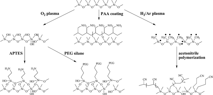
Another major limitation of PDMS as stamp material is its hydrophobic nature. In the seminal work of Whitesides1 on μCP of n-alkyl thiols, this hydrophobicity was well suited. However, when printing more polar molecules, especially biological “inks” such as proteins or DNA, the ink is repelled by the hydrophobic PDMS stamp, which means that the stamp is not sufficiently inked and as a consequence the ink cannot be transferred to the substrate. The hydrophobic nature of PDMS can also result in denaturation and irreversible adsorption of proteins. This problem can be faced either by surface treatment of the PDMS stamps (e.g.oxidation or chemical modification) or by selecting a more polar polymer (e.g.agarose) to prepare a stamp. Fig. 2 provides a selection of polymers and prepolymers that have been used to make stamps for μCP.
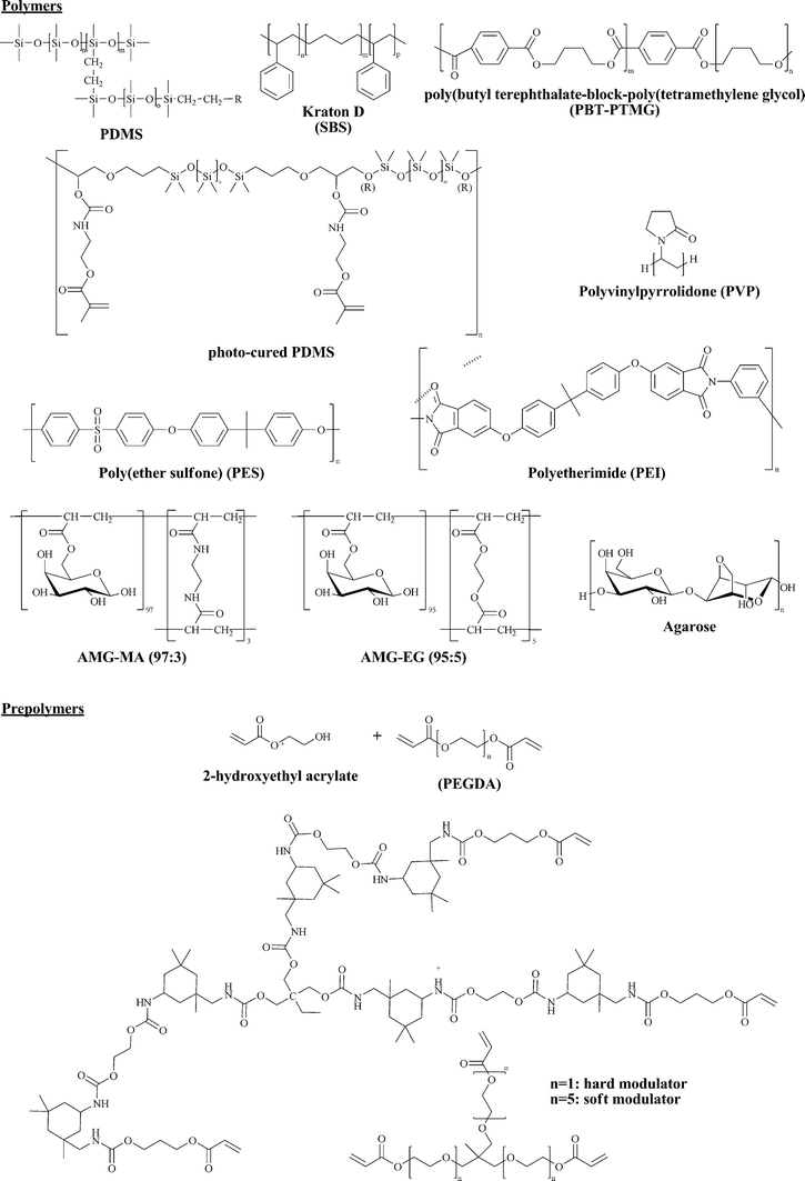 | ||
| Fig. 2 A selection of polymers and prepolymers that have been used in μCP. | ||
2.1. Surface modification of PDMS stamps
PDMS is routinely oxidized by exposing the polymer to UV irradiation at ambient conditions. The mechanism of PDMS oxidation by ozone is not completely understood. It is known that ozone oxidizes the dimethylsiloxane network at the surface and induces the formation of silanolgroups. It is further known that not only the presence of ozone but the combination of ozone and UV-irradiation is responsible for the oxidation and that after longer exposure times the silanolgroups condense with neighbouring silanolgroups to yield Si–O–Si bonds, as verified by IR spectroscopy and XPS.6Oxidation times of up to 30 min (depending on the experimental conditions) are sufficient to obtain homogeneous, hydrophilic PDMS surfaces, whereas longer oxidation times yield a thin surface layer of silica.7
Olander et al. analyzed the mechanism of PDMS oxidation by oxygen plasma.8 By X-ray photoelectron spectroscopy (XPS) measurements they revealed that one methyl group of the dimethylsiloxane units is first substituted by an oxygen atom. This reaction has a half life time of 5 s. After prolonged oxidation, silica like structures formed at the PDMS surface.
It should be emphasized that the hydrophilicity of oxidized PDMS is subject to a phenomenon referred to as “hydrophobic recovery”, which describes the decrease of polarity of PDMS surfaces after oxidation with time. Hydrophobic recovery is due to the tendency to minimize the surface energy of the oxidized polymer and is caused by the flexibility of polymer chains. Hydrophobic recovery occurs on briefly (<30 min) oxidized PDMS as well as on “silica coated” PDMS surfaces, although the process is slower and less homogeneous in the case of prolonged oxidation times.7 Importantly, hydrophobic recovery is fast when oxidized PDMS stamps are exposed to air, and much slower when oxidized PDMS stamps are stored in water.
The transfer of low molecular weight PDMS oligomers during μCP and the effect of PDMS oxidation on this phenomenon has been investigated in detail.9,10 XPS studies on the plasma oxidized PDMS clearly showed that oxygen plasma pre-treatment of the stamps significantly reduces the transfer of PDMS residues on the substrates after printing.
 | ||
| Fig. 3 Polar coatings for PDMS stamps. | ||
Delamarche et al. reacted a PEG silane with an oxidized PDMS stamp.12 The polarity of the hydroxyl-terminated PEG layer was stable for 7 days and the stamps were used to pattern Pd/Sn colloids for ELD of NiB. Furthermore, flat stamps with protein repellent PEG patterns were used for the transfer of proteins from the non-coated (hydrophobic) areas.
Plasma polymerization is another surface treatment to prepare polar PDMS stamps. He et al.13 exposed a PDMS stamp to Ar/H2 plasma, which causes homolysis of a methyl group of the PDMS. The surface radicals can initiate the polymerization of acetonitrile, resulting in a cyano-terminated polymer adlayer. This functionalization was especially useful for biological applications, as the coated stamps showed optimal wetting by acetonitrile, which is a standard DNAsolvent. The modified PDMS stamps showed significantly decreased WCA (30–35°) and the coating was stable for more than one month. A similar way to make amino terminated PDMS stamps was introduced by Sadhu et al. in 2007.14 By means of plasma polymerization of allylamine, they deposited a 5 nm thick poly(allylamine) coating on PDMS (as well as on other polymer stamps). This hydrophilic coating was stable for several months and could be used to transfer very polar molecules such as poly(propylene imine) (PPI) dendrimers from aqueous solution onto various substrates.
A major advance in the resolution of μCP involves a radically altered design of stamps: instead of exploiting the voids in the microrelief pattern as an ink diffusion barrier, it is possible to impose an ink diffusion barrier on a flat PDMS stamp.15 For example, by oxidation of the PDMS surface, a thin silicon oxide film is created, which is essentially impermeable to apolar inks. If the oxidation is directed by a mask, a flat stamp with a surface pattern of silicon oxide on PDMS results. This flat stamp can be used for μCP of n-alkyl thiols, which are transferred exclusively in the non-oxidized area. The properties of the diffusion barrier and the stability of the stamp may be improved by coating the silicon oxide film with a fluorinated silane SAM. Even volatile, low molecular weight inks can be printed with such chemically patterned flat stamps. Moreover, because the stamp is flat, all problems due to deformation of the microrelief surface structures are circumvented. Hence, the resolution of the stamp is now limited only by the resolution of the oxidation mask. Recently, the same group demonstrated the use of nanoimprint lithography (NIL) to prepare flat PDMS stamps that were chemically patterned at the sub-100 nm scale.16 In an alternative approach, the resolution of μCP with flat stamps was extended into the sub-100 nm scale by using dip pen nanolithography (DPN) to “write” a nanostructured oxidation mask on the surface of a flat PDMS stamp.17 Amongst others, the patterns included a nanoscale map of the USA!
2.2. PDMS composite stamps
Composite stamps are composed of at least two different materials. PDMS composite stamps have an increased mechanical stability compared to conventional PDMS stamps. To this end, a thin PDMS stamp can be fixed onto a rigid support such as a glass plate (Fig. 4). This prevents the stamps from sagging, which affects the quality of μCP at the nanoscale or when the interspaces of the pattern become very large. Furthermore, the rigid support reduces long range distortions due to external stress, thermal expansion and swelling in solvents. Composite stamps have been applied by several groups.18–20 The “thickness” of the polymer stamp was reduced to 200 nm19 and patterns of sub-micrometre periodicity in far separated features could be achieved over large areas. The interface of the polymer with the rigid support can be made either by simply pressing a glass slide onto the liquid prepolymer on the mold or by chemical adhesion, employing alkene surface modification.19 Instead of glass, also stiffer polymers like polyimide have been used as support.21 In this case the stamps were used for nanoscale printing.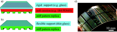 | ||
| Fig. 4 Various architectures of composite stamps: (a) three component, (b) and (c) two component stamp. Copyright Fig. 4c: American Chemical Society, 2000. | ||
A second strategy to increase the mechanical stability of PDMS stamps is to change the silanes used to make the stamps. Schmid et al. used this approach to realize a PDMS modification optimizing the ratio of functional to methyl groups with regard to the mechanical strength of the resulting polymer.22 They (and others23) refer to this PDMS as h-PDMS (“hard PDMS”). They also found that addition of silica particles raises the Young's modulus to ca. 10 MPa. It should be noted that these variations are always a compromise between mechanical strength needed to achieve faithful pattern reproduction with sub-micrometre resolution and flexibility required for conformal contact between the stamp and the substrate. Schmid et al. used h-PDMS as a topmost layer of a three component composite stamp. Underneath the h-PDMS layer they applied a 30 μm thick soft cushion of commercial PDMS attached to a glass plate. This soft layer could balance surface roughness, whereas the h-PDMS layer was stiff enough to replicate submicron patterns. They also presented stamps which consisted of a 5% glass filled, h-PDMS attached to a 100 μm thick and flexible glass back plate (Fig. 4). This example perfectly illustrates the compromises that have to be taken regarding the mechanical properties of stamps for μCP. Both composite stamps were able to accurately replicate 100 nm patterns over large areas (5 × 5 cm2).
Photocurable PDMS with improved physical properties for μCP has been presented in 2003.24 The mechanical strength of this polymer was tuned by adjusting the amount of cross-linker. The optimized polymer had a higher modulus than commercial PDMS yet remained less brittle than h-PDMS. The superior properties of photocurable PDMS were demonstrated by making stamps with 300 nm resolution and high aspect ratio which could not be prepared using conventional PDMS or h-PDMS.
A completely different strategy to realize nanoscale patterns by μCP was used by Bruinink et al.25 Rather than attempting to stabilize positive patterns, they utilized a combination of soft lithography methods to obtain stamps with negative nanopatterns. A silicon substrate was coated with a poly(methyl methacrylate) (PMMA) layer, the substrate was heated to melt the PMMA, and the substrate was contacted with a microstructured PDMS stamp and lifted off the substrate. The PMMA adheres especially to the edges of the stamp due to capillary forces. After cooling to room temperature, an “edge-pattern” in nanometre dimensions is obtained, which can then be used as a second generation master to create negative nanopatterned stamps (i.e. the relief structure points inwards). Using either “positive” or “negative” μCP of thiols on an Au substrate, sub-150 nm patterns could be obtained.
2.3. PDMS alternatives
To overcome the drawbacks of PDMS for μCP – in particular its low polarity and low mechanical stability – stamps can obviously be prepared from other polymers. It should be noted that although the overwhelming majority of publications on μCP involve standard PDMS stamps, a number of interesting alternative have been proposed in recent years (Fig. 2).Trimbach et al. developed a two component polymer, which they could use to print small, hydrophilic, organic inks26 as well as proteins.27 Their thermoplastic polymer blend consisted of a poly(ether-block-ester) (PEE). The stamps were prepared by hot embossing of the solid polymer, avoiding the problem of oligomer/monomer contamination of substrates during the printing process, which is concern when using PDMS as stamp material. The stamps were used to print thiol SAMs on Au substrates as well as bovine serum albumin (BSA) onto NHS ester SAMs. BSA can also be printed using PDMS stamps, but due to the hydrophobicity of PDMS and its poor adsorption of the protein, inking times up to 15 min are required, which could be reduced to 30 s with PEE stamps. A convenient side effect is that also the protein concentration could be reduced significantly due to the optimized interaction between polar stamp and protein ink.
The same group introduced other commercial block copolymers as stamp materials for various applications. They used poly(styrene-block-butadiene-block-styrene) (SBS, Kraton D1102) and poly(styrene-block-ethylene-co-butylene-block-styrene) (SEBS, Kraton G1652) to print thiols on Au.28 The resulting monolayers were dense enough to be used as etch resist. The major advantage of these polyolefins is their higher mechanical strength, which makes them more suitable for printing demanding aspect ratio patterns that would not be feasible using PDMS stamps. These stamps can be loaded with higher weight without pattern deformation to guarantee conformal contact between stamp and substrate.
Polyolefin plastomers (POP) stamps have successfully been used to print proteins (e.g.fibrinogen) and peptidecopolymers at 100 nm resolution.29 Although the POP stamps are of comparable quality to the PDMS stamps (even with 100 nm feature size), the quality of the transferred fibrinogen pattern differed dramatically. Whereas POP transferred patterns were of very good quality, the PDMS patterns suffered strongly from sagging. Further advantages of the POP material were the faster stamp production by hot embossing and the lack of oligomer contamination of the substrates after printing. In addition the stamps could be recycled.
A versatile system of photocurable poly(urethane acrylate) has been developed for molding and printing purposes.30 The additional ethoxy units within the cross-linker increase the elongation at break by a factor of 5 and decrease the Young's modulus by the factor of 16. Although ink diffusion during the printing smeared the line pattern by about 40 nm, distinct separated lines of etched Au in the range of 250 nm could be resolved, which is not possible with standard PDMS.
An inventive approach towards hydrophilic, photocurable polymers has been presented by mixingpoly(ethylene glycol) diacrylate (PEGDA) and a commercial adhesive.31 While the PEGDA provided a polar polymer network that showed excellent wettability and permeability for water and ethanol, the adhesive provided the desired mechanical resistance. Properties like mechanical flexibility and water/ethanol holding capacity could be tuned by choosing the proper mixing ratio. Since the water holding capacity always remained higher than that of standard PDMS, this polymer is better suited for biological applications. This was demonstrated by printing BSA with 2 μm resolution.
One early example of PDMS substitution is the introduction of hydrogel stamps by Martin et al.32 Hydrogels are extremely hydrophilic, water containing but water insoluble polymers, bearing very polar units in the polymer structure (e.g. carbohydrates). Martin et al. optimized the ratio of 6-acryloyl-α-O-methyl-galactopyranoside and one of two crosslinkers (ethylene glycol dimethylacrylate or N,N-α-methylenebisacrylamide) to find a compromise between mechanical strength and gel porosity. Nonetheless, the hydrogel stamps had to be supported with fused silica plates because of their poor mechanical strength. The hydrogel stamps were used to print alkylamine ligands and second generation poly(amidoamine) (G2 PAMAM) dendrimers onto polyvinyl benzyl chloride films spin cast onto Si, and the patterns were made visible by fluorophore attachment. Two years later, the same group reported the use of their hydrogel stamps to print pyridine from aqueous solution onto solvent template chlormethylphenyl coated substrates.33 They prevented ink diffusion by heating the samples immediately after printing, thereby covalently coupling the ink as a pyridinium salt onto the substrate. The pyridine patterns were used to complex Pd particles as nucleation site for ELD of Ni.
Hydrogel stamps were employed by Coq et al. to transfer proteins and antibodies onto solid substrates without significant loss of activity.34 This is challenging since proteins are very sensitive to external conditions. Furthermore, these hydrogel stamps did not require a solid support. This group used a 2-hydroxyethyl acrylate based polymer and poly(ethylene glycol) diacrylate as a cross-linker. The hydrogel stamps showed a remarkable hydrophilicity (WCA = 19°) and a high water/buffer holding capacity (up to 50%). When using highly water loaded stamps (>20%), the stamps showed poor mechanical stability and therefore resulted in bad pattern quality. When using stamps with low water content (<10%), the stamps were mechanically stable, but also brittle because they suffered from dehydration. A water content of 10% was shown to be the optimum, but at the same time comprising enough water to preserve the antibody “ink”. The antibody pattern showed an activity comparable to molecules reacted from solution, which had not been achieved with μCP before. Also the antibodies could be fixed either by adsorption on bare Au surfaces or by grafting them covalently onto NHS ester SAMs.
Agarose gel is another hydrophilic material that has been utilized as stamp material.35–38Agarose is a linear polysaccharide consisting of galactose and 3,6-anhydrogalactose subunits. Agarose gel is obtained by boiling agarose in a buffer and is used for separation of biological polymers such as DNA and proteins by gel electrophoresis. The adaptation for μCP was first reported in 2004.35Agarose stamps were used to print single proteins, protein gradients and even an immunoassay comprising 8 different proteins. One substantial advantage of agarose stamps is their property to act as an ink reservoir. In the case of the printed immunoassay no re-inking of the stamp was necessary during 20 printing cycles without decrease in pattern quality. A further advantage is the fact that only subnanomolar concentrations of the proteins are needed, because of the excellent interaction of the proteins with the stamp material. Agarose stamps have also been used to print human osteoblastcells onto hydroxyapatite scaffolds.36 A similar experiment showed that it is possible to print bacteria.37 In this case the stamp even “re-inked” itself due to bacterial growth on the stamp. After 250 printing cycles, the stamp was left for one week at 25 °C and could then be used for additional printing cycles. This procedure could be repeated for several weeks. It should be noted that the cells did not penetrate the stamps but instead adhere to the stamp surface. Five different cell types could be printed onto substrates after manually dispensing the respective solutions onto the stamp patterns.
Agarose stamps have also been utilized for a completely different purpose: Grzybowski and co-workers used agarose stamps to etch silicon surfaces with HF solution (Fig. 5).38 They were able to faithfully replicate the stamp pattern features in silicon surfaces down to 300 nm. However, also larger patterns were replicated, such as optical lenses with 250 μm diameter as well as 75 μm deep microfluidic channels.
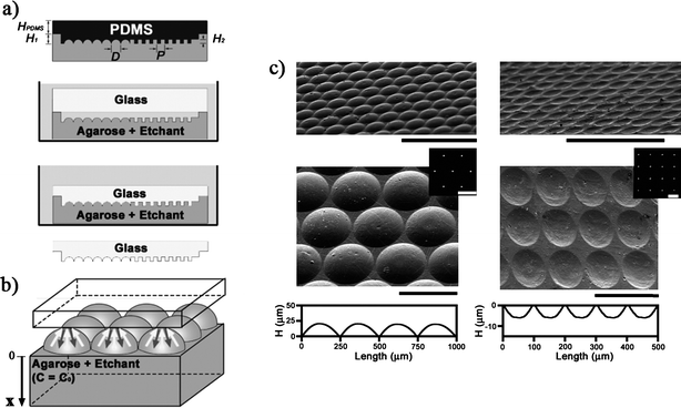 | ||
| Fig. 5 HF etching of glass substrates using agarose stamps. (a) An agarose stamp is made by casting agarose gel (10 wt% in water) against a master, soaked in an HF etchant/surfactant solution, inverted, and immersed in mineral oil. The substrate is placed on top of the stamp. When etching is complete, the substrate is removed, rinsed, and cleaned. (b) Microetching is a result of a two-way pump mechanism, in which the agarose continuously supplies the etchant (white arrows) to dissolve the substrate while absorbing the etching products (gray arrows) into the stamp. (c) Convex (left) and concave (right) microlenses etched in glass. Copyright: Wiley-VCH, 2006. | ||
Recently, a new class of porous μCP stamps was prepared by phase separation micromolding.39 This method relies on the phase separation of a polymer solution on a structured mold. A mixture of polymers cast onto a micromold is placed in a non-solvent (e.g.water) where polymer chains of the soluble component leave the bulk and produce pores filled by the non-solvent. By using such porous stamps, high-molecular-weight polar inks (dendrimers, proteins, and silica NPs) were successfully printed. The pores serve as an ink reservoir for repeated printing steps without re-inking and without loss of printing quality.
3. Polymer inks for microcontact printing
Polymers are particularly useful as inks for μCP, since they tend to adhere strongly to the contact area and diffuse only slowly into non-contact areas. A broad range of polymers – including conducting polymers and biological polymers – have been used as inks for μCP. It could be argued that any polymer can be used as ink for μCP, provided it is soluble so that a suitable μCP stamp can be inked with it. μCP of a polymer ink on a surface yields a microstructured polymer surface in a single printing step. Polymer inks can also be printed on polymer substrates. In this way, μCP can give easy access to organic electronic devices as well as biological microarrays. We have chosen to discriminate the following subcategories of polymer inks in this review: synthetic polymers, dendrimers, and biological polymers such as proteins and DNA. The polymer inks can be attached covalently on reactive surfaces, they can adhere through electrostatic interactions (e.g. in polyelectrolyte layers) or they can be physisorbed on substrates. Although many polymers can be directly transferred to a surface of choice, alternatively an initiator can be printed and the initiator pattern may serve as a template for graft polymerization to yield a microstructured array of dense polymer brushes. Finally it should be mentioned that μCP has also been used extensively to direct polymer adsorption on surfaces, e.g. by printing a hydrophobic/hydrophilic pattern followed by demixing of a polymer blend, selective deposition of one polymer or dewetting of a polymer on the patterned surface. However, since in those cases the polymer has no role in μCP, this application of μCP to microstructure polymers exceeds the scope of this review.3.1. Synthetic polymer inks
An early report on μCP with a polymer ink was published by Jiang and Hammond in 2000.40 They printed a maleic acid terminated poly(ethylene oxide) onto an amine terminated polyelectrolyte multilayer and made use of the pattern for selective deposition of further polyelectrolyte layers. By repeated μCP of different polymers, multilevel architectures could be realized. They also printed poly(acrylic acid) (PAA) as an anionic charge pattern onto poly(allylamine hydrochloride) (PAH)/PAA multilayer substrates in 80 nm resolution using the advantageous strength of electrostatic binding (which prevents ink diffusion) in combination with a stiff, high resolution, UV-curable stamp.41 These charge patterns have subsequently been used for the patterned deposition of anionic PS nanospheres. Also hydrophobic copolymers can be printed, resulting in a hydrophilic/hydrophobic pattern.42Another straightforward method to create polymer patterns on substrates has been introduced using a combined hot embossing/μCP technique.43 A layer of polymer was deposited on a flat PDMS stamp and the pattern feature was created by hot embossing with a negative polymer master. Afterwards the pattern consisting solely of the polymer to be transferred was brought into contact with the substrate and transferred by heating above the glass transition temperature (Tg) of the transferred polymer (Fig. 6). Glycerol was used as adhesion promoter on solid substrates. This technique was used to create polymer/fullerene photodiodes on (3,4-ethylenedioxythiophene)/poly(4-styrenesulfonate) (PEDOT:PSS) films with superior performance regarding quantum efficiency and dark current. PEDOT:PSS has also been patterned with μCP to build organic light emitting devices (LEDs)44 and thin film transistors (TFTs).45Polymers like poly(ether sulfone) (PES), poly(ethylene terephthalate) (PET) and poly(vinyl chloride) (PVC) have been used as substrates. Also polythiophenes have been printed onto Au coated surfaces.46
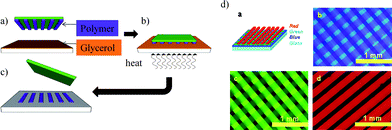 | ||
| Fig. 6 Transfer printing of luminescent polymers. (a) The polymer is patterned by hot embossing and transferred onto a flat PDMS stamp, (b) the patterned polymer is contacted with a PEDOT:PSS film wetted with glycerol, (c) the polymer is transferred from stamp to substrate upon heating, (d) patterns of luminescent polymers obtained by μCP. Copyright Fig. 6d: Wiley-VCH, 2008. | ||
Other free-standing polymer devices have been fabricated using μCP. Thin film polypropylmethacrylate (PPMA) particles have been realized by printing the polymer with a microstructured PDMS stamp onto a sacrificial poly(vinyl alcohol) (PVA) layer.47 After dissolution of the PVA, the quasi 2 D objects could be analyzed by AFM. Isolated azo polymer microwires have been fabricated in a very similar manner. However, instead of dissolving a sacrificial polymer layer the uppermost glass layer was etched away using HF solution.48
μCP of hybrid materials comprising Fe NPs absorbed in a diblock copolymer was used to create micropatterns of NPs on a surface.49 The copolymer could be etched by oxygen plasma either on the loaded stamp or after transferring the composite onto the substrate. A way to grow carbon nanotubes directly onto a surface by polymer assisted iron catalyst patterning has been presented by Hammond.50 They were able to grow multiwalled carbon nanotubes on Al2O3 coated surfaces by printing Fe loaded PS-block-PAA micelles onto the surface, subsequently etching the polymer by oxygen plasma and then using the Fe pattern as nucleation sites for the growth of carbon nanotubes. A related approach of polymer directed patterns of inorganic material has been used to create TiO2 patterns.51 To this end, a dispersion of a TiO2 NPs and poly(styrene-alt-maleic acid) was applied to PDMS stamps. The dewetting of the dispersion on the stamp leads to the formation of disk shaped composites which then could be transferred to the substrates. Calcination was used to get rid of the polymer yielding a regular pattern of TiO2. Topographical dewetting on patterned stamps has also been applied to transfer patterns of polymers (hydrolyzed poly(styrene-alt-maleic anhydride) copolymer, PS or PEO) onto Au, Si and polymer substrates.52
Synthetic polymers have also been used as inks in μCP with regard to biological applications. One challenge is to print a simple polymer template for cell adhesion. Poly(-L-lysine) (PLL) has proven to be suitable for such purposes. Wheeler and co-workers transferred PLL using PDMS stamps coated with a release layer of detergent.53 This resulted in optimized loading and transfer properties of the stamps. The success of the surface patterning was shown by selective attachment and growth of hippocampal cells. Similarly, RGD functionalized PEG-PLL copolymer patterns directed the adhesion of various cell types.54 Non-selective cell attachment was prevented by backfilling of the printed patterns with the unmodified copolymer, as PEG is a commonly used material for cell repellence. Other reports have been published using μCP of PEG copolymers like poly((3-trimethoxysilyl)propyl methacrylate-r-poly(ethylene glycol))55 and poly(ethylene glycol)-branched-poly(methyl methacrylate).56 It has also been shown that μCP of poly(sulfonic acids) can be used for directed attachment of cells.57 Attachment of hepatocytes could be shown on patterns of PSS, poly(vinylsulfonic acid) and poly(anetholesulfonic acid). A similar approach, employing a pattern of positively and negatively charged synthetic polymers on polyelectrolyte multilayers for the simultaneous and selective binding of hepatocytes (anionic pattern of PSS) and fibroblasts (positive pattern of PAH) without loss of viability has been reported.58μCP of polyphosphazenes have also been used for site selective attachment and growth of human cells (neuroblastoma).59 Fluorinated or regular oligo(ethylene glycol) phosphazenes showed significant cell repellence, whereas the incorporation of aromatic and acid moieties resulted in increased cell affinity. Apart from their biological properties they could also be used as insulating or conducting patterns, respectively, which can be useful not only for interfaces of electric circuits and neurons but also for the development of microelectrode arrays. Another interesting way of printing polymers for biological experiments is to utilize hydrophobic patterns of (intentional) PDMS “residues” and PMMA structures created by μCP on a surface for the stretched alignment of DNA strands.60 Also pre-oriented (stretched) DNA molecules on a PDMS stamp could be transferred retaining their configuration. One interesting example for applications in molecular electronics was the stretched DNA strand conjugated with a semiconducting, thiophene based polyelectrolyte.
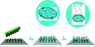
3.2. Polymer brushes from initiator inks
Polymer brushes are of current interest in polymer surface science. Polymer brushes are linear polymers that are aligned normal to and stretch away from the surface. The microscale control of the spatial arrangements of such polymer brushes enables a local functionalization of the surface with densely packed and covalently attached polymers. Two different approaches exist: the first is called the “grafting from” (or “bottom up”) approach and involves the local grafting of initiator molecules followed by polymerization at the surface. Provided the initiator can be immobilized in a high density, also the polymer brush can be grown in a high density (Fig. 7). An alternative approach is the so-called “grafting to” (or “top down”) approach. This term is used to describe the immobilization of polymers on the surface. The “grafting to” strategy often results in less densely packed brushes because the polymer molecules must diffuse through the initial brush layer onto the surface. On the other hand, the “grafting to” method has the advantage of avoiding the polymerization reaction on the surface, which is often severely hindered compared to the solution polymerization.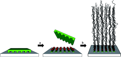 | ||
| Fig. 7 Creating structured polymer brushes by μCP (“grafting from” approach): (a) μCP of the initiator, (b) graft-polymerization on initiator patterns. | ||
One early example of combining the “grafting from” strategy with μCP was a report of Nuzzo and co-workers61 They used a printed OTS pattern as mask for the backfilling of the interspaces with a norbornenyl terminated chlorosilane as initiator for ring-opening metathesispolymerization (ROMP). These polymer brushes could afterwards be used as masks for reactive ion etching. The polymer length could be tuned by modifying monomer concentration and reaction time. This “indirect” approach of printing an unreactive mask, backfilling the pattern with initiator molecules and then starting the polymerization has been employed by various groups. Apart from ROMP this method has been used in combination with ring-opening polymerization,62 atom transfer radical polymerization (ATRP),63,64 and electropolymerization.65 The alternative way of directly printing patterns of initiator molecules has also been shown to be successful for building polymer brushes using free radical polymerization,66chemical vapour deposition (CVD) polymerization,67–69ROMP,70photopolymerization,71 biopolymerization with peroxidase,72 anodic polymerization73,74 and ATRP.75–77 The resulting polymer brush patterns have been successfully employed to direct cell attachment,66 to template hydrogels,71 to pattern liquid crystalline phases78 and conductive polymer patterns,69,73,74 to prepare 2D polymer-Au hybrid objects,76 and to induce the formation of calcite crystal patterns.79 One recent report by Huck and co-workers demonstrated the versatility of printed initiators for polymer brush formation as they were able to print up to 4 different initiators one after the other (Fig. 8).75 This proved that the bare Au surface left within the interspaces of one initial pattern is still available for further modification, e.g. for yet another printing cycle of initiator molecules. Also this technique was compatible with very different polymerization reactions such as cationic, anionic and neutral polymerizations.
 | ||
| Fig. 8 Multibrush patterned surfaces comprising one (a), two (b), three (c) and four (d) different brushes on the same substrate. Copyright American Chemical Society, 2006. | ||
One further example for the use of grafting from strategy in μCP has employed Au NP arrays coated with a thiol grafted initiator for ATRP of N-isopropylacrylamide.80 The Au NPs were adsorbed from solution onto a substrate (glass, PS, silicon, Au) patterned with a sacrificial polymer mask by μCP. After removal of the polymer mask, polymerization was initiated yielding stimuli responsive polymer brushes.
Also the “grafting to” method has been adapted to μCP. Park and Thomas printed a rod-coil copolymer terminated bearing triethoxysilyl moieties for covalent attachment onto Si substrates and analyzed the resulting structures by AFM.81 A stimuli responsive (in this case: solvent responsive) brush pattern was created using two very different polymers. First, an adhesive layer of 3-glycidoxypropyl trimethoxysilane was spin coated onto Si wafers. The substrates were then immersed into a solution of acid functionalized PS to react with the epoxide terminated silane. During μCP of the second polymer, poly(2-vinyl pyridine), this polymer diffused through the PS layer to react with vacant epoxides of the silane. Applying different solvents (toluene and ethanol), only one of the brushes swelled due to preferential solvation.
3.3. Dendrimer inks
Dendrimers are versatile inks for μCP due to the high density of end groups at their periphery, which results in efficient multivalent interaction with nearly any substrate. In addition, dendrimers are the ink of choice for high resolution μCP.The first report on dendrimer inks used for μCP was published in 2002.82 Huck and co-workers printed patterns of G4 PAMAM dendrimers on Si substrates. During 5 s of contact time between the inked stamp and the substrate, monolayer patterns (1 nm height) were formed with 70 nm lateral resolution. Almost at the same time a second report was published about the influence of ink concentration on multilayer formation during μCP of PAMAM dendrimers.83 It was found that when PAMAM dendrimer inks of concentrations higher than 0.1 mM were used for μCP, the pattern height could be as much as 40 nm, which indicates multilayer formation. These multilayers were stable against rinsing and even sonication. It was postulated that the stability of the printed dendrimer layers might be due to cross-linking of the dendrimers with CO2 under ambient conditions. PAMAM patterns have also been intentionally cross-linked by modification of the dendrimers with methoxysilane moieties.84 These methoxysilanes were used graft the dendrimers onto Si substrates and cross-link to adjacent dendrimers. The cross-linked patterns were stable for several days.
A different strategy to create stable poly(propylene imine) (PPI) dendrimer patterns on surfaces made use of multivalent host–guest interactions of adamantane (guest) modified dendrimers and cyclodextrin (host) SAMs on Au and glass substrates (“molecular printboards”).85 The multiple noncovalent host–guest interactions resulted in superior stability of the printed patterns. Guest dendrimers were also used as “supramolecular glues” for binding Au NPs as catalyst for ELD of Cu on the structured surfaces. The versatility of these host–guest patterns has been demonstrated in further experiments.86 Anionic fluorescent dyes were encapsulated in the dendrimers, and dyes could be exchanged while the guest dendrimers were patterned on the host monolayer (Fig. 9).
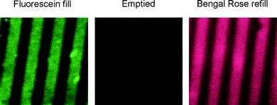 | ||
| Fig. 9 Reversible filling of μCPdendrimer structures with an anionic dye, emptying by rinsing with buffer and refilling with a second anionic dye. Copyright Wiley-VCH, 2005. | ||
The dendrimers could also be filled by printing a dye on the immobilized dendrimers. It was shown that it is possible to create supramolecular layer by layer (LBL) structures on host SAMs with guest functionalized PPIdendrimers and subsequent deposition of β-cyclodextrin coated Au NPs.87 Also, it was possible to print redox active dendrimer patterns using ferrocene as guest groups on PPIdendrimers.88 By locally oxidizing the ferrocene-PPI dendrimers on the substrate using scanning electrochemical microscopy (SECM), the dendrimers could selectively be removed because oxidized Fc+ moieties are not suitable guests for β-CD.
Another approach to printing G3 PPIdendrimers on Au surfaces has been realized by sulfide functionalization of the dendrimers.89 The sulfides on the dendrimer form strong coordinative bonds to Au surfaces and thereby further reduce the diffusion of these heavy weight molecules. For this reason these inks could be deposited with 100 nm resolution and used as positive patterns for wet etching. This is caused by the fact that the dendrimer patterns are permeable for etching solutions so that after backfilling the PPI patterns with ODT, wet etching occurs selectively underneath the dendrimer patterns.
Dendrimers (and proteins) could be printed with very high resolution using V-shaped h-PDMS stamps.90,91 The quality of the stamps in combination with the high molecular weight ink was sufficient to yield 40 nm patterns which could be used as templates for directed Au NP deposition and as etching masks to obtain Pdnanowires when the dendrimers were printed onto Pd coated substrates. With a similar application in mind, Kern and co-workers used patterns of hydroxyl terminated G4 PAMAM dendrimers on nonconducting substrates as hosts for Pd2+-ions, which in turn could be exploited as nucleation sites for ELD of Co.92 Kern and co-workers also reported the use of CdS/G8 PAMAM clusters as inks in μCP on hydrophilic Si substrates.93 The dendrimers fulfil two capacities at the same time: they act as a hydrogen-bonding glue to the surface and they stabilize the CdS NPs. However, it was observed the CdS NPs tend to cluster and show Ostwald ripening. Thereby the size, which in turn determines the photo yield, of the printed NP clusters can be controlled in the range of 10 to 60 nm. This effect has been exploited in a later experiment: even when flat stamps were used for μCP, the formation of line patterns could be observed (“bottom up inside top down patterning”).94
3.4. Biological polymer inks
μCP can provide biological microarrays in a straightforward manner because many biological polymers such as proteins or DNA are suitable inks for μCP. The first report about μCP of proteins dates from 1998.95μCP of proteins can be very simple: inking of a PDMS stamp with aqueous protein solution, incubation, air-drying of the stamp and conformal contact of the stamp with the substrate. The rather large molecular weight of “biological inks” enhances the formation of well-defined, high-contrast patterns since their diffusion is limited. The transfer of biopolymers from the stamp to the substrate by μCP depends on the surfaces properties of the stamp and the substrate. The simplest μCP approach for patterning of biopolymers relies on the direct transfer of ink molecules adsorbed on the stamp to a target substrate by conformal contact. Several important factors have to be considered for μCP of biopolymers. The affinity of the biopolymer to stamp and to substrate must be tailored so that it is higher for the substrate than for the stamp. μCP should not cause denaturation, so hydrophobic stamps and substrates are best avoided in μCP of proteins. Ideally, the biopolymer should be printed in the way that it will expose all the active sites to the target molecules. It should be mentioned that μCP has also been used extensively to direct biopolymer adhesion on surfaces, e.g. by printing a hydrophobic/hydrophilic pattern followed by selective deposition of the biopolymer on the patterned surface. However, since in that case the biopolymer itself is not involved in μCP, this application of μCP exceeds the scope of this review.Biotin is a small molecule that binds strongly to streptavidin and avidin. These strong interactions are frequently used in bionanotechnology. A general scheme for the application of biotin in the context of μCP is depicted in Fig. 10. Chilkoti et al. used μCP to pattern biotin terminated ethylene glycol amine molecules onto PET activated with a surface layer of an active ester.96 Subsequently, specific binding of fluorescently labelled streptavidin could be observed on the biotin patterns. μCP was also used to print biotin on a SAMs of active esters on an Au substrate, subsequently binding biotin patterns to fluorescent antibodies.97 μCP and the biotin-streptavidin (or avidin) interaction have also been exploited to create cell patterns on biodegradable polymer substrates bearing biotin moieties.98
 | ||
| Fig. 10 Printing biotin ligands onto a substrate and subsequent binding of streptavidin or avidin which can be used to direct the immobilization of further biotinylated molecules. | ||
Antibodies have been printed onto various surfaces using physisorption as binding force.95,99 Even patterns of single proteins (antibodies and green fluorescent protein) could be realized by a sophisticated μCP technique.100Antibodies can be transferred onto oxidized glass substrates yielding even higher surface coverage of proteins than in comparable absorption experiments from solution.101 Another study explicitly focused on the effect of the printing process on antibody selectivity (i.e. activity) and concluded that only minor decrease in functionality resulted after μCP of antibodies onto oxidized glass substrates.102 However, a prior report on enzyme activity of galactose oxidase and horseradish peroxidase patterns on Au and glass surfaces created by μCP concluded that printing an OTS mask and backfilling the pattern with a thiol modified enzyme is better suited for remaining the protein activity than direct μCP of the enzyme or application of the enzyme by microfluidics.103
Besides antibodies and enzymes also many other proteins have been used as inks in μCP. Choi and co-workers used cytochrome C as ink,104 whereas the group of Rinaldi printed metallo proteins.105 Delamarche and co-workers demonstrated the remarkable result of printing up to 16 different proteins onto PS samples without loss of activity using a flat stamp inked with microfluidics.106
Furthermore, μCP of proteins is not restricted to substrates such as Au, glass and PS: Saavedra et al. showed that polymerized lipid bilayers can be used as substrates for μCP of proteins with high surface coverage.107 Fibronectin and even mammalian cells have been printed onto PS substrates108 as well as chemically modified myosin. Myosin patterns have been used to direct actin filament polymerization which can be interesting for guiding the movements of biomolecular motors.109 Indeed the direction of filament polymerization could be controlled as long as the filament did not approach the border of the “bio highways” in a too high angle. Kennedy and co-workers developed an efficient microarray immunoassay for phenoxybenzoic acid (PBA) which is a biomarker of human exposure to insecticides.110 The microarray was obtained by μCP of BSA-PBA onto glass slides which then could locally bind antibodies for PBA, attached to highly fluorescent Eu![[thin space (1/6-em)]](https://www.rsc.org/images/entities/char_2009.gif) :Gd2O3 NPs encapsulated in PLL.
:Gd2O3 NPs encapsulated in PLL.
One last, very elegant way of printing proteins deserves to be highlighted. The group of Delamarche presented a μCP strategy which they called “affinity contact printing” (Fig. 11).111 In affinity contact printing, a flat, aminosilane coated PDMS stamp is locally modified with proteins (antigens) by microspotting using a microwell mask. The biochemical pattern on the stamp can subsequently be used for transferring target proteins (antibodies). The automated microspotting enables the application of a wide variety of proteins on the same stamp which is a perfect qualification for the construction of protein microarrays. The relative complicated stamp fabrication is balanced by the possibility to reuse the same stamp several times.
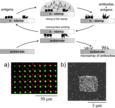 | ||
| Fig. 11 Affinity contact printing relies on inking the surface of a PDMS stamp with antigens as “capture molecules” and subsequent binding of selected antibodies from a solution containing mixtures of proteins. (a) A fluorescence microscopy image showing the transfer of TRITC-anti-chicken and FITC-anti-goat antibodies from a stamp onto a glass substrate. (b) An AFM image obtained on a spot of the array in which printed anti-goat antibodies bound to Au-labelled goat antigens presented in solution. Binding was detected by staining the Au labels with ELD of Ag NPs of an average diameter of 80 nm. Copyright Wiley-VCH, 2002. | ||
DNA can also be patterned by μCP. The group of Bernard showed that μCP of DNA onto APTES modified surfaces has some advantages over the more routinely used microspotting of DNA solutions.112 They demonstrated that printed pattern features lack the typical rims observed in spotted patterns due to solvent evaporation (“coffee stain effect”) and that several arrays could be produced with a single stamp, whereas spotting is a serial process and every device is an original that has to be manufactured individually. DNA has also been printed onto bare hydrophobic substrates like PS and silanized glass after derivatization to “DNAsurfactants”, that means amphiphilic DNA.113 To this end, a hydrophobic anchoring group has been attached to the DNA strands that fixed the molecule using hydrophobic interactions with the substrate and at the same time improved wetting properties of the DNA ink regarding the hydrophobic PDMS surface. Another strategy has been used by the group of Reinhoudt et al.114 They modified oxidized PDMS stamps with G5 PPIdendrimers which yielded a positive surface charge on the stamp. These “dendristamps” could be used to print the negatively charged DNA and RNA strands, avoiding the “coffee stain effect”. The grafting was done covalently by printing amino-modified DNA and RNA onto an aldehyde SAM on glass supports, yielding imine bonds that were subsequently reduced to secondary amine bonds. The DNA microarrays could be hybridized with complementary DNA. Furthermore a flat dendrimer coated stamp could be modified with a chemical pattern of hundreds of different DNA strands by spotting technique which could be used to print DNA microarrays. The stamps could be reused 3 to 4 times (Fig. 12). The Reinhoudt group also showed that DNA grafting could be done using click chemistry without a CuIcatalyst.115 To this end, alkyne-modified nucleotides were included in the DNA and printed onto an azide terminated SAM.
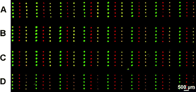 | ||
| Fig. 12 A DNA microarray replicated four times by μCP using robotic microspotting to ink the stamp. The stamp was coated with PPIdendrimers to increase the adhesion of the DNA. Copyright American Chemical Society, 2007. | ||
Finally, it has been shown that DNA as well as polypeptides can be synthesized on a surface by repeated μCP cycles. A 20-meroligonucleotide was synthesized by repeated μCP with protected nucleotides to induce the reaction using phosphoramidite chemistry on the surface.116 The successful synthesis has been underlined by the intentional incorporation of mismatched bases, which cause a decreasing hybridization of the oligonucleotide sequence. Moreover, Huck and co-workers described the formation of peptides by printing N-protected amino acids onto an amine-terminated SAM on Au.117 Of course, peptide bonds do not spontaneously form from carboxylic acids and amines under ambient conditions, and it was proposed that “the nanoscale confinement of the ink at the interface between the stamp and the SAM, in combination with the pre-organization of the reactants in the SAM, facilitates the formation of covalent bonds”.117 In a remarkable experiment, it was shown that the consecutive μCP of as many as 20 peptide nucleobases resulted in the formation of an oligopeptidenucleic acid that could selectively bind a complementary strand of DNA. These findings point to the fascinating potential of surface chemistry by μCP: complex biomacromolecules can be synthesized simply by printing the monomers in the appropriate sequence!
4. Polymer substrates for microcontact printing
The third major application of polymers in μCP is the use of polymer substrates. A number of superior properties of polymer substrates compared to “traditional” substrates for μCP (metals, glass, Si wafers) make them especially attractive for electronic and biotechnological applications. For a start, many polymers are easy to process in thin foils or as coatings under mild conditions, and they are often flexible and transparent. In contrast, solid substrates are often difficult to process, and they are brittle and non-transparent. Moreover, most polymers are insulators, which make them useful as material for circuit boards or other non-conductive components of electronic devices. In contrast, substrates like metals, ITO or Si are (semi-) conductors. For biological applications polymers can be of interest if they are mechanically flexible, biocompatible and can be deposited as a coating on other substrates. In addition, the surface properties of polymers can be tailored by choosing the proper (mixture of) monomers. In combination with μCP, the surface properties of polymers can be customized at the microscale in a straightforward manner. The adhesion of ink to a polymer substrate can occur in a non-covalent or a covalent fashion.4.1. Non-covalent immobilization on polymer substrates
Metals can be microstructured on polymeric substrates via μCP in combination with ELD. Metal NPs (mostly Pd) serve as catalytic nucleation sites for deposition of a second metal (often Ni or Cu) from a solution containing a reducing agent. Whitesides and co-workers printed Pd colloids directly on a range of polymer substrates which were pre-treated with APTES.118 Complex metal structures could be obtained after Cu deposition, which could even be released as free-standing metal objects after dissolution of the polymer substrate. These 2D metal structures could be shrunk in size by annealing the printed Pd coated polymer substrates slightly above their Tg.119 A similar approach has been used by Moran et al. for ELD of Ni structures on PS substrates.120 They applied a combination of embossing and μCP when they heated the stamp during the printing of polymer stabilized Pd NPs, thereby molding a structure at the same time that they established the Pd pattern in the molds. After ELD of Ni, metal features down to 1 μm could be realized. μCP has also been applied in the fabrication of an organic TFT on polyethylene naphthalate (PEN) foil.121 The PEN substrate was pre-treated with tetramethyl ammonia hydroxide solution to form surface hydroxyl functions and patterned with a hydrophobic silane template to direct complexation of Pd(II) in unmodified areas. Subsequent reduction to Pd(0) and ELD of Ni provided a gate electrode for the TFT. The complete TFT was then constructed on the basis of this gate electrode with low cost processing, flexible mechanical properties and good performance.Optical waveguides have been printed in phloxine B doped poly(4-vinylphenol) substrates by “electrical μCP”.122 To this end, an Au coated stamp with the waveguide pattern was brought into contact with the substrate and the applied current locally bleached phloxine B. The pattern of bleached phloxine Bpolymer formed the cladding for unbleached substrate parts representing the waveguide core for guiding light in the wavelength range from 600 to 1310 nm. Another report describes the formation of charge patterns on PMMA substrates by μCP.123 Other polymer optical devices include colloidal crystals of PS and silica microspheres by μCP, using a PVA substrate as a thermal glue to fix the colloids by heating the polymer slightly above its Tg.124 This technique was compatible even with non-planar surfaces such as glass tubes.
Complex patterns on the inside of polymer tubes could be realized by μCP on polymeric substrates.125 A polymer bilayer of PS and poly(styrene-block-4-vinyl pyridine) was patterned via μCP (e.g. with Au NPs), after which the polymer substrate was cut into pieces, released from the solid support and rolled up by choosing a solvent that swells the lower layer but not the upper one. This method is an interesting way to induce chirality in 3D polymer substrates.
Polymer substrates are of interest in biotechnological applications. The most effective polymer for cell and protein repellence is PEG. A copolymer of PEG and poly(lactic acid) (PLA) has been used to direct protein repulsion on PS substrates by μCP of PLA-PEG onto the PS substrate followed by backfilling with BSA.126 In this way, μCP of BSA – which often results in denaturation of the protein and hence loss of functionality – could be circumvented. PLA-PEG is also an excellent example of the design of polymers combining cell repellent properties (PEG) with biodegradability (PLA). A very similar experiment described the patterning of a PLA substrate with non-adhesive poly(oligoethylene glycol methacrylate) (poly-OEGMA) to control cell attachment and morphology.127 Also a combination of two biodegradable polymers was used for selective cell attachment and the control of cell proliferation and morphology.128 In this case, poly(DL-lactic-co-glycolic acid) and a PEG-PLA copolymer were used. Either of the two polymers could be used as substrate coating and afterwards be spatially modified with the other polymer by μCP.
Micropatterns of extracellular matrixproteins such as laminin and fibronectin on polymer substrates are useful to investigate cell adhesion and motility. Plasma deposited films of non-fouling tetraethylene glycol dimethyl ether on polymer and glass substrates have been used for μCP of laminin and subsequent binding and spreading of cardiomyocytecells on the laminin pattern.129Laminin has also been used to print patterns on plasma activated PMMA substrates for the later control of Schwann and nerve cell adhesion and proliferation.130 Chilkoti et al. printed patterns of fibronectin on a non-fouling comb polymer comprising a methacrylate backbone and EG based side chains.131 This polymer becomes cell repellent upon contact with water, because only then the EG chains cover the surface. Fibronectin patterns were also used for experiments regarding the combination of topographical (hot embossing) and chemical (μCP) patterns on polyimide substrates. If only one pattern was present, adhesion of osteoblastcells followed the structural as well as the chemical pattern. When both patterns were present (perpendicular to each other), the topographical pattern dominated.
Also hydrogels can be functionalized with biological molecules. For example, a hydrogel coating containing disulfides has been patterned with iodoacetyl biotin by μCP to attach streptavidin which in turn can bind additional biotinylated molecules.132 Using this approach, proteins that are not suitable as inks for μCP can be attached to these patterns. Other proteins, like the famous green fluorescent protein as well as the red fluorescent protein were used as inks for μCP on hydrogels.133
A complementary technique of “erosive” patterning was presented in 2005. A report demonstrated the possibility of printing lipase solution on poly(trimethylene carbonate) films for local enzymatic degradation of the polymer.134
Another interesting polymer substrate in biological applications is chitosan, which is a natural poly amino-saccharide. Kumar et al. used this polymer as substrate for selective cell and protein deposition after patterning the substrates with the highly cell repellent OEGMA. To fix the non-adhesive polymer mask on the chitosan substrate, a random copolymer was prepared with methacrylic acid, which exhibits strong acid–base interactions with the amino functionalized biopolymer. The patterns could be used to adhere cells in a oriented way and guide filament spreading.135
4.2. Covalent immobilization on polymer substrates
μCP can also be used to induce chemical reactions on a surface. In principle, almost any bimolecular reaction that is possible in solution can also be conducted on a surface by μCP. In fact, many reactions are much faster under μCP conditions than in solution. Although this method is also known as “reactive μCP”, we refer to this method as “microcontact chemistry”, in particular when it involves molecules that are typically unreactive.136Polymers are excellent substrates for covalent patterning by μCP. Most reactions of polymer substrates involve of reactive carboxylic acid derivatives such as pentafluorophenol (PFP) or N-hydroxysuccinimide (NHS) esters (Fig. 13).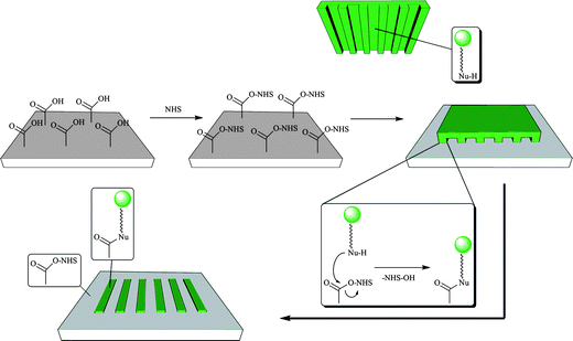 | ||
| Fig. 13 μCP of nucleophilic inks (typically: amines) on active ester derivatized polymer surfaces (typically: N-hydroxysuccinimide esters) leading to the formation of amide (peptide) bonds exclusively in the area of contact between stamp and substrate. | ||
Ghosh and Crooks printed hexadecylamine on anhydride activated PE.137 To this end, the PE surface was oxidized with CrO3/H2O/H2SO4 and converted into an anhydride by treatment with N-methylmorpholine. The alkylamine pattern on the PE substrate was used as a mask for local grafting of poly(acrylic acid).
Yang and Chilkoti prepared PFPester terminated PET films and printed biotin ligands on those polymer substrates.138 In later work they also used polymer substrates like PE, PS and PMMA.139 Similar reactions but different polymerizations were used by Langer and co-workers140PFP activated PGA films have been used to covalently attach the tripeptideRGD.141 Patterns of cell and protein resistant PEG-amine were printed on the activated esterpolymer as a mask which afterwards was used to locally bind RGD from solution in the pattern interspaces. Fluorescently labelled cells could be shown to preferentially adsorb on those RGD patterns. A second experiment made use of the biotin-streptavidin interaction after μCP of NH2-biotin on the activated surface. A more sophisticated experiment was reported in 2006:142 a microreactor array consisting of aligned polyelectrolyte multilayer capsules was prepared on a PFP activated PET surface. After μCP of avidin on the activated surface, biotinylated PSS/PAH multilayer capsules were selectively attached on the avidin patterns. These capsules could then be used for particle synthesis and the leaching could be controlled (and even blocked) by the number of polyelectrolyte layers. This makes the microarray attractive for drug release and targeting studies.
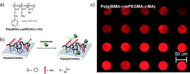
Amino-PEG has also been printed on NHS polymer surfaces as a mask for BSA and DNA grafting.143 The interpattern NHS-activated surface remains active for post-functionalization and the adsorbed biomolecules preserve their functionality. Choi and co-workers used a bromo-terminated SAM on Au and silicon substrates as initiators for ATRP of OEGMA, on which hydroxy terminated side chains could later be NHS-activated and serve as a reactive coating for μCP of biotin and poly-L-lysine.144 The success was demonstrated by selective binding of streptavidin and cells. In another publication the same group used a polymer containing PEG as well as NHS functionality as a reactive coating on amino-SAMs on Au.145 Part of the NHS groups served as covalent links to the amine surface. Residual NHS groups were then used to pattern amino-biotin by μCP which could afterwards be complexed by streptavidin. The same experiment was possible on silicon substrates when adding a polymer block containing trimethoxysilylgroups for surface grafting.146 Also PS substrates coated with an amphiphilic three component polymer have recently been employed for this strategy, using hydrophobic blocks as anchors, PEG blocks as repellent against unspecific adsorption and an acid terminated polymer block for NHS functionalization.147 On these substrates NH2-biotin as well as a protein has been printed (Fig. 14). These examples describe μCP strategies involving polymers that show three properties which can be tuned easily by controlling the mixing ratio of monomers: they contain surface grafting sites (NHS, alkoxysilanes or hydrophobic anchors), they are bio-inert (PEG side chains) and yet comprise reactive sites (NHS or carboxylic acid functions).
 | ||
| Fig. 14 Grafting of a three-component polymer on polymer substrates by μCP. Copyright American Chemical Society, 2007. | ||
Interesting work on tert-butyl acrylate (tBA) based copolymers has been reported by the group of Schönherr. They published several examples of (local) deprotection of the tBA moiety in PS-PtBAcopolymers by trifluoro acetic acid (TFA), conversion of the resulting carboxylic acid into an NHS ester and subsequent further derivatization. One report described a combined imprinting/contact printing approach, first furnishing the polymer substrate with a relief structure by imprinting, deprotecting the tBA units by soaking in TFA, activating the acid moieties with NHS and finally printing fibronectin or BSA on the topographically structured, chemically activated polymer substrate using a flat stamp.148 The non-contacted area was made cell repelling by grafting NH2-PEG molecules inside the structure wells. Subsequent cell seeding resulted in selective attachment and growth of the cells along the chemical and topographic patterns. The advantage of this combination of imprinting and contact printing is the possibility to obtain very small structures that cannot be made by conventional μCP. The same group also induced patterned acrylate deprotection by μCP with TFA.149,150
A rare example of “microcontact chemistry” on a polymer substrate that does not involve carboxylic acid derivatives and amines used click chemistry. Diethynyl[2,2]paracyclophane films were deposited by CVD as a substrate for deposition of a thin layer of azide modified biotin and sodium ascorbate as a reducing agent. CuSO4 was then printed as the catalyst for “click”-reaction. The catalytically active Cu(I) species was obtained in situ by reduction of the Cu(II) through the ascorbate. The biotin patterns could be used for controlled immobilization of streptavidin. One further example of polymer surface chemistry by μCP has recently been reported by Griesser and co-workers151 They used pulsed plasma polymerized films of an epoxy polymer on which they printed lysozyme directly with a flat stamp.
5. Outlook
Polymers play a key role in μCP. They have been employed in μCP in every conceivable way, i.e. as stamp, as ink and as substrate. There are also many examples of μCP in which the stamp and the ink and the substrate are a polymer. μCP is a straightforward method for the preparation of microstructured and nanostructured polymer surfaces.Stamps used for μCP invariably consist of an elastomer polymer, because the stamp must be flexible yet mechanically stable. Only polymers can meet these requirements. The stamp material can be optimized for every μCP experiment. Although the overwhelming majority of publications on μCP still involve conventional PDMS stamps, a number of interesting alternative materials have been proposed. In our view, the most promising developments in this area include the preparation of hydrogel and agarose stamps for μCP of “biological” inks, the preparation of porous stamps for μCP of high molecular weight and NP inks, and the preparation of flat, chemically patterned PDMS stamps for nanocontact printing (i.e.μCP at a scale below 100 nm).
Polymers are versatile inks for μCP. Biological, conductive, electroluminescent, polyelectrolyte or simple insulating polymers can be transferred onto surfaces via μCP. μCP with polymer inks provides microstructured polymer surfaces in a single printing step. In this way, μCP can give easy access to organic electronic devices as well as biological microarrays. In this area we expect increasing application of μCP of functional polymers to provide functional microstructured polymer surfaces.
Finally, polymers are suitable substrates for μCP. Polymer thin films and coatings are especially attractive for electronic and biotechnological applications. In combination with μCP, the surface properties of polymer foils and coatings can be customized at the microscale in a straightforward manner. μCP of polymers on polymer substrates gives direct access to functional microstructured polymer surfaces. We anticipate that μCP will also be increasingly used for the covalent modification of polymer surfaces with micro- and nanostructured molecular monolayers.
References
- A. Kumar and G. M. Whitesides, Appl. Phys. Lett., 1993, 63, 2002–2004 CrossRef.
- A. Perl, D. N. Reinhoudt and J. Huskens, Adv. Mater., 2009, 21, 2257–2268 CrossRef CAS.
- J. Mehlich and B. J. Ravoo, in Nanostructured surfaces, ed. L. Chi, Wiley-VCH, 2010, in press Search PubMed.
- S. A. Ruiz and C. S. Chen, Soft Matter, 2007, 3, 168–177 RSC.
- D. J. Graham, D. D. Price and B. D. Ratner, Langmuir, 2002, 18, 1518–1527 CrossRef CAS.
- V.-M. Graubner, R. Jordan, O. Nuyken, B. Schnyder, T. Lippert, R. Kotz and A. Wokaun, Macromolecules, 2004, 37, 5936–5943 CrossRef CAS.
- H. Hillborg, N. Tomczak, A. Olah, H. Schönherr and G. J. Vancso, Langmuir, 2004, 20, 785–794 CrossRef CAS.
- B. Olander, A. Wirsén and A.-C. Albertsson, J. Appl. Polym. Sci., 2004, 91, 4098–4104 CrossRef CAS.
- B. A. Langowski and K. E. Uhrich, Langmuir, 2005, 21, 6366–6372 CrossRef CAS.
- K. Glasmastar, J. Gold, A.-S. Andersson, D. S. Sutherland and B. Kasemo, Langmuir, 2003, 19, 5475–5483 CrossRef.
- C. Donzel, M. Geissler, A. Bernard, H. Wolf, B. Michel, J. Hilborn and E. Delamarche, Adv. Mater., 2001, 13, 1164–1167 CrossRef CAS.
- E. Delamarche, C. Donzel, F. S. Kamounah, H. Wolf, M. Geissler, R. Stutz, P. Schmidt-Winkel, B. Michel, H. J. Mathieu and K. Schaumburg, Langmuir, 2003, 19, 8749–8758 CrossRef CAS.
- Q. He, Z. Liu, P. Xiao, R. Liang, N. He and Z. Lu, Langmuir, 2003, 19, 6982–6986 CrossRef CAS.
- V. B. Sadhu, A. Perl, M. Peter, D. I. Rozkiewicz, G. Engbers, B. J. Ravoo, D. N. Reinhoudt and J. Huskens, Langmuir, 2007, 23, 6850–6855 CrossRef CAS.
- R. B. A. Sharpe, D. Burdinski, J. Huskens, H. J. W. Zandvliet, D. N. Reinhoudt and B. Poelsema, J. Am. Chem. Soc., 2005, 127, 10344–10349 CrossRef CAS.
- X. Duan, Y. Zhao, A. Perl, E. Berenschot, D. N. Reinhoudt and J. Huskens, Adv. Mater., 2009, 21, 2798–2802 CrossRef CAS.
- Z. Zheng, J.-W. Jang, G. Zheng and C. A. Mirkin, Angew. Chem., Int. Ed., 2008, 47, 9951–9954 CrossRef CAS.
- C. D. James, R. C. Davis, L. Kam, H. G. Craighead, M. Isaacson, J. N. Turner and W. Shain, Langmuir, 1998, 14, 741–744 CrossRef CAS.
- M. Tormen, T. Borzenko, B. Steffen, G. Schmidt and L. W. Molenkamp, Appl. Phys. Lett., 2002, 81, 2094–2096 CrossRef CAS.
- M. Tormen, T. Borzenko, B. Steffen, G. Schmidt and L. W. Molenkamp, Microelectron. Eng., 2002, 61–62, 469–473 CrossRef CAS.
- E. Menard, L. Bilhaut, J. Zaumseil and J. A. Rogers, Langmuir, 2004, 20, 6871–6878 CrossRef CAS.
- H. Schmid and B. Michel, Macromolecules, 2000, 33, 3042–3049 CrossRef CAS.
- T. W. Odom, J. C. Love, D. B. Wolfe, K. E. Paul and G. M. Whitesides, Langmuir, 2002, 18, 5314–5320 CrossRef CAS.
- K. M. Choi and J. A. Rogers, J. Am. Chem. Soc., 2003, 125, 4060–4061 CrossRef CAS.
- C. M. Bruinink, M. Péter, M. de Boer, L. Kuipers, J. Huskens and D. N. Reinhoudt, Adv. Mater., 2004, 16, 1086–1090 CrossRef CAS.
- D. C. Trimbach, M. Al-Hussein, W. H. de Jeu, M. Decre, D. J. Broer and C. W. M. Bastiaansen, Langmuir, 2004, 20, 4738–4742 CrossRef CAS.
- D. C. Trimbach, H. Stapert, J. van Orselen, K. D. Jandt, C. W. M. Bastiaansen and D. J. Broer, Adv. Eng. Mater., 2007, 9, 1123–1128 CrossRef.
- D. Trimbach, K. Feldman, N. D. Spencer, D. J. Broer and C. W. M. Bastiaansen, Langmuir, 2003, 19, 10957–10961 CrossRef CAS.
- G. Csucs, T. Kunzler, K. Feldman, F. Robin and N. D. Spencer, Langmuir, 2003, 19, 6104–6109 CrossRef CAS.
- P. J. Yoo, S.-J. Choi, J. H. Kim, D. Suh, S. J. Baek, T. W. Kim and H. H. Lee, Chem. Mater., 2004, 16, 5000–5005 CrossRef CAS.
- N. Y. Lee, J. R. Lim, M. J. Lee, J. B. Kim, S. J. Jo, H. K. Baik and Y. S. Kim, Langmuir, 2006, 22, 9018–9022 CrossRef CAS.
- B. D. Martin, S. L. Brandow, W. J. Dressick and T. L. Schull, Langmuir, 2000, 16, 9944–9946 CrossRef CAS.
- S. L. Brandow, T. L. Schull, B. D. Martin, D. C. Guerin and W. J. Dressick, Chem.–Eur. J., 2002, 8, 5363–5367 CrossRef CAS.
- N. Coq, T. van Bommel, R. A. Hikmet, H. R. Stapert and W. U. Dittmer, Langmuir, 2007, 23, 5154–5160 CrossRef CAS.
- M. Mayer, J. Yang, I. Gitlin, D. H. Gracias and G. M. Whitesides, Proteomics, 2004, 4, 2366–2376 CrossRef CAS.
- M. M. Stevens, M. Mayer, D. G. Anderson, D. B. Weibel, G. M. Whitesides and R. Langer, Biomaterials, 2005, 26, 7636–7641 CrossRef CAS.
- D. B. Weibel, A. Lee, M. Mayer, S. F. Brady, D. Bruzewicz, J. Yang, W. R. DiLuzio, J. Clardy and G. M. Whitesides, Langmuir, 2005, 21, 6436–6442 CrossRef CAS.
- C. J. Campbell, S. K. Smoukov, K. J. M. Bishop, E. Baker and B. A. Grzybowski, Adv. Mater., 2006, 18, 2004–2008 CrossRef CAS.
- H. Xu, X. Y. Ling, J. van Bennekom, X. Duan, M. J. W. Ludden, D. N. Reinhoudt, M. Wessling, R. G. H. Lammertink and J. Huskens, J. Am. Chem. Soc., 2009, 131, 797–803 CrossRef CAS.
- X. Jiang and P. T. Hammond, Langmuir, 2000, 16, 8501–8509 CrossRef CAS.
- J. Park, Y. S. Kim and P. T. Hammond, Nano Lett., 2005, 5, 1347–1350 CrossRef CAS.
- X. Jiang, H. Zheng, S. Gourdin and P. T. Hammond, Langmuir, 2002, 18, 2607–2615 CrossRef CAS.
- L. Chen, P. Degenaar and D. D. C. Bradley, Adv. Mater., 2008, 20, 1679–1683 CrossRef CAS.
- T. Granlund, T. Nyberg, L. S. Roman, M. Svensson and O. Inganäs, Adv. Mater., 2000, 12, 269–273 CrossRef CAS.
- D. Li and L. J. Guo, Appl. Phys. Lett., 2006, 88, 063513 CrossRef.
- L. Zhai, D. W. Laird and R. D. McCullough, Langmuir, 2003, 19, 6492–6497 CrossRef CAS.
- J. Guan, A. Chakrapani and D. J. Hansford, Chem. Mater., 2005, 17, 6227–6229 CrossRef CAS.
- B. Liu, Y. He and X. Wang, Langmuir, 2006, 22, 10233–10237 CrossRef CAS.
- S.-H. Yun, B.-H. Sohn, J. C. Jung, W.-C. Zin, M. Ree and J. W. Park, Nanotechnology, 2006, 17, 450–454 CrossRef CAS.
- R. D. Bennett, A. J. Hart, A. C. Miller, P. T. Hammond, D. J. Irvine and R. E. Cohen, Langmuir, 2006, 22, 8273–8276 CrossRef CAS.
- M. Wang, H.-G. Braun and E. Meyer, Chem. Mater., 2002, 14, 4812–4818 CrossRef CAS.
- M. Wang, H. G. Braun, T. Kratzmüller and E. Meyer, Adv. Mater., 2001, 13, 1312–1317 CrossRef CAS.
- J. C. Chang, G. J. Brewer and B. C. Wheeler, Biomaterials, 2003, 24, 2863–2870 CrossRef CAS.
- G. Csucs, R. Michel, J. W. Lussi, M. Textor and G. Danuser, Biomaterials, 2003, 24, 1713–1720 CrossRef CAS.
- P. Kim, S. E. Lee, H. S. Jung, H. Y. Lee, T. Kawai and K. Y. Suh, Lab Chip, 2006, 6, 54–59 RSC.
- K. Na, J. Jung, B. Shin and J. Hyun, Langmuir, 2006, 22, 10889–10892 CrossRef CAS.
- S. Kidambi, I. Lee and C. Chan, J. Am. Chem. Soc., 2004, 126, 16286–16287 CrossRef CAS.
- Srivatsan Kidambi, L. Sheng, M. L. Yarmush, M. Toner, I. Lee and C. Chan, Macromol. Biosci., 2007, 7, 344–353 CrossRef CAS.
- E. W. Barrett, M. V. B. Phelps, R. J. Silva, R. P. Gaumond and H. R. Allcock, Biomacromolecules, 2005, 6, 1689–1697 CrossRef CAS.
- P. Björk, S. Holmström and O. Inganäs, Small, 2006, 2, 1068–1074 CrossRef.
- N. L. Jeon, I. S. Choi, G. M. Whitesides, N. Y. Kim, P. E. Laibinis, Y. Harada, K. R. Finnie, G. S. Girolami and R. G. Nuzzo, Appl. Phys. Lett., 1999, 75, 4201–4203 CrossRef CAS.
- M. Husemann, D. Mecerreyes, C. J. Hawker, J. L. Hedrick, R. Shah and N. L. Abbott, Angew. Chem., Int. Ed., 1999, 38, 647–649 CrossRef.
- R. R. Shah, D. Merreceyes, M. Husemann, I. Rees, N. L. Abbott, C. J. Hawker and J. L. Hedrick, Macromolecules, 2000, 33, 597–605 CrossRef CAS.
- H. Tu, C. E. Heitzman and P. V. Braun, Langmuir, 2004, 20, 8313–8320 CrossRef CAS.
- F. S. Marikkar, C. Carter, K. Kieltyka, J. W. F. Robertson, C. Williamson, A. Simmonds, R. Zangmeister, T. Fritz and N. R. Armstrong, Langmuir, 2007, 23, 10395–10402 CrossRef CAS.
- J. Hyun and A. Chilkoti, Macromolecules, 2001, 34, 5644–5652 CrossRef CAS.
- K. Tsukagoshi, W. Mizutani, H. Tokumoto, T. Miyamae and H. Nozoye, Surf. Sci., 2002, 514, 48–53 CrossRef CAS.
- H.-G. Choi, J. P. Amara, T. M. Swager and K. F. Jensen, Langmuir, 2007, 23, 2483–2491 CrossRef CAS.
- J.-Y. Kim, M.-H. Kwon, J.-T. Kim, S. Kwon, D.-W. Ihm and Y.-K. Min, J. Phys. Chem. C, 2007, 111, 11252–11258 CrossRef CAS.
- Y. Harada, G. S. Girolami and R. G. Nuzzo, Langmuir, 2003, 19, 5104–5114 CrossRef CAS.
- S. Kızılel, V. H. Perez-Luna and F. Teymour, Langmuir, 2004, 20, 8652–8658 CrossRef CAS.
- P. Xu, H. Uyama, J. E. Whitten, S. Kobayashi and D. L. Kaplan, J. Am. Chem. Soc., 2005, 127, 11745–11753 CrossRef CAS.
- G. Zotti, S. Zecchin, B. Vercelli, A. Berlin, S. Grimoldi, L. Groenendaal, R. Bertoncello and M. Natali, Chem. Mater., 2005, 17, 3681–3694 CrossRef CAS.
- G. Zotti, B. Vercelli and A. Berlin, Acc. Chem. Res., 2008, 41, 1098–1109 CrossRef CAS.
- F. Zhou, Z. Zheng, B. Yu, W. Liu and W. T. S. Huck, J. Am. Chem. Soc., 2006, 128, 16253–16258 CrossRef CAS.
- J. E. Comrie and W. T. S. Huck, Langmuir, 2007, 23, 1569–1576 CrossRef CAS.
- S. Edmondson, C.-D. Vo, S. P. Armes and G.-F. Unali, Macromolecules, 2007, 40, 5271–5278 CrossRef CAS.
- P. J. Hamelinck and W. T. S. Huck, J. Mater. Chem., 2005, 15, 381–385 RSC.
- Y.-Y. Kim, E. P. Douglas and L. B. Gower, Langmuir, 2007, 23, 4862–4870 CrossRef CAS.
- Jaeyoen Jung, K. W. Kim, K. Na, M. Kaholek, S. Zauscher and J. Hyun, Macromol. Rapid Commun., 2006, 27, 776–780 CrossRef CAS.
- J.-W. Park and E. L. Thomas, J. Am. Chem. Soc., 2002, 124, 514–515 CrossRef CAS.
- H. Li, D.-J. Kang, M. G. Blamire and W. T. S. Huck, Nano Lett., 2002, 2, 347–349 CrossRef CAS.
- D. Arrington, M. Curry and S. C. Street, Langmuir, 2002, 18, 7788–7791 CrossRef CAS.
- N. Kohli, P. R. Dvornic, S. N. Kaganove, R. M. Worden and I. Lee, Macromol. Rapid Commun., 2004, 25, 935–941 CrossRef CAS.
- C. M. Bruinink, C. A. Nijhuis, M. Péter, B. Dordi, O. Crespo-Biel, T. Auletta, A. Mulder, H. Schönherr, G. J. Vancso, J. Huskens and D. N. Reinhoudt, Chem.–Eur. J., 2005, 11, 3988–3996 CrossRef CAS.
- S. Onclin, J. Huskens, B. J. Ravoo and D. N. Reinhoudt, Small, 2005, 1, 852–857 CrossRef CAS.
- O. Crespo-Biel, B. Dordi, P. Maury, M. Peter, D. N. Reinhoudt and J. Huskens, Chem. Mater., 2006, 18, 2545–2551 CrossRef CAS.
- C. A. Nijhuis, J. K. Sinha, G. Wittstock, J. Huskens, B. J. Ravoo and D. N. Reinhoudt, Langmuir, 2006, 22, 9770–9775 CrossRef CAS.
- A. Perl, M. Peter, B. J. Ravoo, D. N. Reinhoudt and J. Huskens, Langmuir, 2006, 22, 7568–7573 CrossRef CAS.
- H.-W. Li, B. V. O. Muir, G. Fichet and W. T. S. Huck, Langmuir, 2003, 19, 1963–1965 CrossRef CAS.
- S. G. Jang, D.-G. Choi, S. Kim, J.-H. Jeong, E.-S. Lee and S.-M. Yang, Langmuir, 2006, 22, 3326–3331 CrossRef CAS.
- X. C. Wu, A. M. Bittner and K. Kern, Langmuir, 2002, 18, 4984–4988 CrossRef CAS.
- X. C. Wu, A. M. Bittner and K. Kern, Adv. Mater., 2004, 16, 413–417 CrossRef CAS.
- A. M. Bittner, X. C. Wu, S. Balci, M. Knez, A. Kadri and K. Kern, Eur. J. Inorg. Chem., 2005, 2005, 3717–3728 CrossRef.
- A. Bernard, E. Delamarche, H. Schmid, B. Michel, H. R. Bosshard and H. Biebuyck, Langmuir, 1998, 14, 2225–2229 CrossRef CAS.
- Z. Yang, A. M. Belu, A. Liebmann-Vinson, H. Sugg and A. Chilkoti, Langmuir, 2000, 16, 7482–7492 CrossRef CAS.
- J. Lahiri, E. Ostuni and G. M. Whitesides, Langmuir, 1999, 15, 2055–2060 CrossRef CAS.
- N. Patel, R. Bhandari, K. M. Shakesheff, S. M. Cannizzaro, M. C. Davies, R. Langer, C. J. Roberts, S. J. B. Tendler and P. M. Williams, J. Biomater. Sci., Polym. Ed., 2000, 11, 319–331 CrossRef CAS.
- P. M. St. John, R. Davis, N. Cady, J. Czajka, C. A. Batt and H. G. Craighead, Anal. Chem., 1998, 70, 1108–1111 CrossRef.
- J. P. Renault, A. Bernard, A. Bietsch, B. Michel, H. R. Bosshard, E. Delamarche, M. Kreiter, B. Hecht and U. P. Wild, J. Phys. Chem. B, 2003, 107, 703–711 CrossRef CAS.
- J. R. LaGraff and Q. Chu-LaGraff, Langmuir, 2006, 22, 4685–4693 CrossRef CAS.
- D. J. Graber, T. J. Zieziulewicz, D. A. Lawrence, W. Shain and J. N. Turner, Langmuir, 2003, 19, 5431–5434 CrossRef CAS.
- T. Wilhelm and G. Wittstock, Langmuir, 2002, 18, 9485–9493 CrossRef CAS.
- S. K. Kwak, G. S. Lee, D. J. Ahn and J. W. Choi, Mater. Sci. Eng., C, 2004, 24, 151–155 CrossRef.
- A. Biasco, D. Pisignano, B. Krebs, R. Cingolani and R. Rinaldi, Synth. Met., 2005, 153, 21–24 CrossRef CAS.
- A. Bernard, J. P. Renault, B. Michel, H. R. Bosshard and E. Delamarche, Adv. Mater., 2000, 12, 1067–1070 CrossRef CAS.
- E. E. Ross, J. R. Joubert, R. J. Wysocki, K. Nebesny, T. Spratt, D. F. O'Brien and S. S. Saavedra, Biomacromolecules, 2006, 7, 1393–1398 CrossRef CAS.
- E. Entcheva and H. Bien, Lab Chip, 2005, 5, 179–183 RSC.
- K. A. Interliggi, W. L. Zeile, S. A. Ciftan-Hens, G. E. McGuire, D. L. Purich and R. B. Dickinson, Langmuir, 2007, 23, 11911–11916 CrossRef CAS.
- M. Nichkova, D. Dosev, S. J. Gee, B. D. Hammock and I. M. Kennedy, Anal. Chem., 2005, 77, 6864–6873 CrossRef CAS.
- J. P. Renault, A. Bernard, D. Juncker, B. Michel, H. R. Bosshard and E. Delamarche, Angew. Chem., Int. Ed., 2002, 41, 2320–2323 CrossRef CAS.
- S. A. Lange, V. Benes, D. P. Kern, J. K. H. Horber and A. Bernard, Anal. Chem., 2004, 76, 1641–1647 CrossRef CAS.
- C. Xu, P. Taylor, M. Ersoz, P. D. I. Fletcher and V. N. Paunov, J. Mater. Chem., 2003, 13, 3044–3048 RSC.
- D. I. Rozkiewicz, W. Brugman, R. M. Kerkhoven, B. J. Ravoo and D. N. Reinhoudt, J. Am. Chem. Soc., 2007, 129, 11593–11599 CrossRef CAS.
- D. I. Rozkiewicz, J. Gierlich, G. A. Burley, K. Gutsmiedl, T. Carell, B. J. Ravoo and D. N. Reinhoudt, ChemBioChem, 2007, 8, 1997–2002 CrossRef CAS.
- P. F. Xiao, N. Y. He, Z. C. Liu, Q. G. He, X. Sun and Z. H. Lu, Nanotechnology, 2002, 13, 756–762 CrossRef CAS.
- T. P. Sullivan, M. L. v. Poll, P. Y. W. Dankers and W. T. S. Huck, Angew. Chem., Int. Ed., 2004, 43, 4190–4193 CrossRef CAS.
- P. C. Hidber, W. Helbig, E. Kim and G. M. Whitesides, Langmuir, 1996, 12, 1375–1380 CrossRef CAS.
- P. C. Hidber, P. F. Nealey, W. Helbig and G. M. Whitesides, Langmuir, 1996, 12, 5209–5215 CrossRef CAS.
- W. K. Ng, L. Wu and P. M. Moran, Appl. Phys. Lett., 2002, 81, 3097–3099 CrossRef CAS.
- U. Zschieschang, H. Klauk, M. Halik, G. Schmid and C. Dehm, Adv. Mater., 2003, 15, 1147–1151 CrossRef CAS.
- D. B. Wolfe, J. C. Love, B. D. Gates, G. M. Whitesides, R. S. Conroy and M. Prentiss, Appl. Phys. Lett., 2004, 84, 1623–1625 CrossRef CAS.
- T. Cao, Q. Xu, A. Winkleman and G. M. Whitesides, Small, 2005, 1, 1191–1195 CrossRef CAS.
- X. Yan, J. Yao, G. Lu, X. Chen, K. Zhang and B. Yang, J. Am. Chem. Soc., 2004, 126, 10510–10511 CrossRef CAS.
- V. Luchnikov, O. Sydorenko and M. Stamm, Adv. Mater., 2005, 17, 1177–1182 CrossRef CAS.
- W. Inglis, G. H. W. Sanders, P. M. Williams, M. C. Davies, C. J. Roberts and S. J. B. Tendler, Langmuir, 2001, 17, 7402–7405 CrossRef CAS.
- C.-C. Lin, C. C. Co and C.-C. Ho, Biomaterials, 2005, 26, 3655–3662 CrossRef CAS.
- L. Lu, K. Nyalakonda, L. Kam, R. Bizios, A. Göpferich and A. G. Mikos, Biomaterials, 2001, 22, 291–297 CrossRef CAS.
- Y. V. Pan, T. C. McDevitt, T. K. Kim, D. Leach-Scampavia, P. S. Stayton, D. D. Denton and B. D. Ratner, Plasmas Polym., 2002, 7, 171–183 CrossRef CAS.
- K. E. Schmalenberg, H. M. Buettner and K. E. Uhrich, Biomaterials, 2004, 25, 1851–1857 CrossRef CAS.
- H. Ma, J. Hyun, Z. Zhang, J. T. P. Beebe and A. Chilkoti, Adv. Funct. Mater., 2005, 15, 529–540 CrossRef CAS.
- M. R. Burnham, J. N. Turner, D. Szarowski and D. L. Martin, Biomaterials, 2006, 27, 5883–5891 CrossRef CAS.
- J. P. Park, K.-B. Lee, S. J. Lee, T. J. Park, M. G. Kim, B. H. Chung, Z.-W. Lee, I. S. Choi and S. Y. Lee, Biotechnol. Bioeng., 2005, 92, 160–165 CrossRef CAS.
- Z. Zhang, S. Zou, G. J. Vancso, D. W. Grijpma and J. Feijen, Biomacromolecules, 2005, 6, 3404–3409 CrossRef CAS.
- G. Kumar, Y. C. Wang, C. Co and C.-C. Ho, Langmuir, 2003, 19, 10550–10556 CrossRef CAS.
- B. J. Ravoo, J. Mater. Chem., 2009, 19, 8902–8906 RSC.
- P. Ghosh and R. M. Crooks, J. Am. Chem. Soc., 1999, 121, 8395–8396 CrossRef CAS.
- Z. Yang and A. Chilkoti, Adv. Mater., 2000, 12, 413–417 CrossRef CAS.
- J. Hyun, Y. Zhu, A. Liebmann-Vinson, T. P. Beebe and A. Chilkoti, Langmuir, 2001, 17, 6358–6367 CrossRef CAS.
- J. Lahann, I. S. Choi, J. Lee, K. F. Jensen and R. Langer, Angew. Chem., Int. Ed., 2001, 40, 3166–3169 CrossRef CAS.
- K.-B. Lee, D. J. Kim, Z.-W. Lee, S. I. Woo and I. S. Choi, Langmuir, 2004, 20, 2531–2535 CrossRef CAS.
- B. Wang, Q. Zhao, F. Wang and C. Gao, Angew. Chem., Int. Ed., 2006, 45, 1560–1563 CrossRef CAS.
- C. L. Feng, G. J. Vancso and H. Schönherr, Adv. Funct. Mater., 2006, 16, 1306–1312 CrossRef CAS.
- B. S. Lee, Y. S. Chi, K.-B. Lee, Y.-G. Kim and I. S. Choi, Biomacromolecules, 2007, 8, 3922–3929 CrossRef CAS.
- B. S. Lee, S. Park, K.-B. Lee, S. Jon and I. S. Choi, Biointerphases, 2007, 2, 136–142 CAS.
- S. Park, K.-B. Lee, I. S. Choi, R. Langer and S. Jon, Langmuir, 2007, 23, 10902–10905 CrossRef CAS.
- D. Sung, S. Park and S. Jon, Langmuir, 2009, 25, 11289–11294 CrossRef CAS.
- A. Embrechts, C. L. Feng, C. A. Mills, M. Lee, I. Bredebusch, J. Schnekenburger, W. Domschke, G. J. Vancso and H. Schönherr, Langmuir, 2008, 24, 8841–8849 CrossRef CAS.
- C. L. Feng, G. J. Vancso and H. Schönherr, Langmuir, 2007, 23, 1131–1140 CrossRef CAS.
- C. L. Feng, A. Embrechts, I. Bredebusch, J. Schnekenburger, W. Domschke, G. J. Vancso and H. Schönherr, Adv. Mater., 2007, 19, 286–290 CrossRef CAS.
- B. Thierry, M. Jasieniak, L. C. P. M. de Smet, K. Vasilev and H. J. Griesser, Langmuir, 2008, 24, 10187–10195 CrossRef CAS.
| This journal is © The Royal Society of Chemistry 2010 |