Ligand-assisted fabrication of hollow CdSe nanospheres via Ostwald ripening and their microwave absorption properties
Minhua
Cao
*a,
Huiqin
Lian
b and
Changwen
Hu
*a
aKey Laboratory of Cluster Science, Ministry of Education of China, Department of Chemistry, Beijing Institute of Technology, Beijing, 100081, P. R. China. E-mail: caomh@bit.edu.cn; Fax: +86 (10) 6891263; Tel: +86 (10) 6891263
bDepartment of Mechanical and Electrical Engineering, Beijing University of Chemical Technology, Beijing, 100029, P. R. China
First published on 22nd October 2010
Abstract
Hollow CdSe nanospheres were successfully synthesized by a ligand-assisted solvothermal method based on an Ostwald ripening mechanism. The hollow CdSe nanospheres were synthesized in benzyl alcohol under solvothermal conditions using Cd(Ac)2 and Se as the precursors, and tryptophan as a ligand. The resulting hollow structures consisted of small nanocrystallite building blocks. More importantly, the hollow CdSe nanospheres could be used as an excellent microwave absorber for cm- and mm-wave absorption, depending on the thickness of the absorber.
1. Introduction
Recently, hollow inorganic micro- and nanomaterials have received increasing attention in many areas of modern science and technology because of their applications in drug delivery, catalysis, adsorption, separation, microreactors and photonic devices.1–4 Manipulation of the structure and morphology of hollow materials on a nm-scale would give the possibility of achieving control of their local chemical environment.5 The fabrication of this type of material generally involves the use of hard or soft templates.6–9 However, the template approach usually suffers from disadvantages such as high cost and tedious synthetic procedures that result from the removal of hard templates and a weakened functionality of the obtained hollow nanomaterials owing to absorbed surfactants by the soft method. In addition to the template method, a significant breakthrough in the fabrication of hollow nanostructures was the use of various known physical phenomena, such as oriented attachment,10 Ostwald ripening11 and the Kirkendall effect,1 in which mass transport via Ostwald ripening has proved to be a facile approach to producing hollow nanomaterials. This ripening process involves “the growth of large particles by sacrificing small aggregates” that have a higher solubility than the larger ones. Compared with templating synthesis, it shows great flexibility for generating different types of hollow nanostructures, including core–shell and multiple shell spaces.12 However, to the best of our knowledge, there are only a few reports on the synthesis of hollow CdSe nanostructures.13 Therefore, the synthesis of well-defined CdSe hollow structures remains a challenge.CdSe semiconductor nanocrystals have attracted considerable attention in recent years because of their size- and shape-dependent optical and electronic properties.14,15 Much more effort has been focused on the synthesis of monodispersed CdSe nanocrystals with tunable luminescent properties. These pioneering investigations have provided deep insights into both the chemistry and physics of CdSe nanocrystals, but there is still a great and challenging issue to be addressed, i.e. developing their novel applications. Recently, microwave absorbing materials have attracted extensive interest due to their potential applications in various fields, especially in electromagnetic interference shielding and radar systems. Magnetic materials are one of the promising microwave absorbing materials because of their high specific resistance, and fascinating magnetic and electromagnetic properties. Most work has been focused on reducing the size of magnetic nanomaterials or compositing magnetic components with electronic ones to improve their microwave absorbing properties. In addition, since carbon nanotubes were discovered by Iijima in 1991, they have been shown to exhibit a good microwave absorbing performance by dielectric loss, and a “geometrical effect” has been ascribed to this behavior.16 Up to now, only a few reports have been concerned with the study of morphology-dependent microwave absorbing properties.17,18,19a In this article, we report not only the synthesis of well-defined hollow CdSe nanospheres, but also our initial findings of the new application of hollow CdSe nanospheres as microwave absorbers. In addition, morphology-dependent microwave absorption properties were observed in our examples.
Herein, we report a ligand-assisted solvothermal synthesis of CdSe hollow nanostructures based on an Ostwald ripening mechanism. The hollow CdSe nanospheres were synthesized in benzyl alcohol under solvothermal conditions using Cd(Ac)2 and Se as the precursors and tryptophan as a ligand. The benzyl alcohol was used not only as a solvent, but also as a reducing agent. More importantly, we demonstrate that the hollow CdSe nanospheres could be used as an excellent microwave absorber for cm- and mm-wave absorption, depending on the thickness of the absorber.
2. Experimental section
2.1. General synthesis
In a typical synthesis, 0.04 mmol Cd(Ac)2 and 0.04 mmol Se powder were added to benzyl alcohol (20 mL) and stirred at room temperature for 0.5 h. Then, 2 mL of a tryptophan aqueous solution (0.005 M) was added into the above suspension. The mixture was then transferred into a 25 mL Teflon™-lined autoclave and sealed and heated at 150 °C for 36 h. After the reaction, the final brown product was collected by filtration, washed with deionized water and alcohol to remove any possible ionic remnants, and then dried in a vacuum at room temperature.2.2. Characterization
The composition and phase purity of the as-synthesized samples were analyzed by XRD with monochromatized Cu-Kα (λ = 1.54178 Å) incident radiation by a Shimadzu XRD-6000 instrument operating at 40 kV voltage and 50 mA current. The size and morphology of the samples were characterized by a JEOL JSM-6700F field-emission SEM. A JEOL JEM-2010F transmission electron microscope operating at a 200 kV accelerating voltage was used for TEM, HRTEM and SAED analyses. FT-IR spectra were recorded on an IFS 28/B FT-IR spectrometer (Bruker Analytik). XPS analyses were carried out using a KRATOS 165 Ultra photoelectron spectrometer with a monochromatic Al-Kα (hυ = 1486.6 eV) radiation source. All binding energies were calibrated by referencing to C1s (285.0 eV). The hollow CdSe nanospheres and solid nanoparticles/paraffin composite samples were prepared by uniformly mixing the hollow nanospheres or nanoparticles in a paraffin matrix and then pressing the mixture into a cylindrically-shaped compact (∅outer = 7.00 mm and ∅inner = 3.04 mm). The electromagnetic (EM) parameters of the composite samples with 70 wt% of the hollow or solid sample were measured in the 2–18 GHz range using an Agilent E8362B vector network analyzer.3. Results and discussion
A typical powder X-ray diffraction (XRD) pattern of the as-synthesized powder formed via a ligand-assisted solvothermal synthesis is shown in Fig. 1a. All the resolved diffraction peaks can be assigned to zinc blende CdSe (JCPDS no. 19-0191) without any indication of crystalline by-products such as Se, SeO2 or CdO. Although wurtzite CdSe is considered to be the thermodynamically favored phase, a zinc blende CdSe phase is still obtained by the solvothermal method, while the reported zinc blende CdSe phase was synthesized by using a strong complexing agent in a strongly alkaline environment.19c It is thought that the strong chelation between Cd2+ and the complexing agent may be the reason for the formation of zinc blende CdSe.19c In our case, although the mechanism for the formation of zinc blende CdSe is still under investigation, we think it is also related to the use of a tryptophan complexing agent.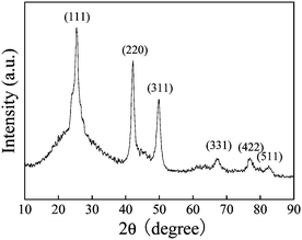 | ||
| Fig. 1 The XRD pattern of the hollow CdSe nanospheres. | ||
In our system, only reducing benzyl alcohol solvent was used and no additional reducing agent was introduced. To prove whether or not benzyl alcohol could completely reduce the Se powder to Se2−, X-ray photoelectron spectroscopy (XPS) was performed, as shown in Fig. 2. The peaks located at 405.3 and 55.4 eV are assigned to Cd 3d5/2 (Fig. 2a) and Se 3d (Fig. 2b), respectively, which is in agreement with previously reported values for CdSe nanocrystals.19b This implies that Se2− exists in the final product, not SeO2 or Se. In addition, this reducing process has also been confirmed by comparing the Fourier transform infrared spectrum (FT-IR) of the CdSe sample with that of benzyl alcohol, as shown in Fig. 3. The band at 1699 cm−1 is characteristic of C![[double bond, length as m-dash]](https://www.rsc.org/images/entities/char_e001.gif) O stretching, which points to the fact that benzyl alcohol is partly oxidized into benzaldehyde.
O stretching, which points to the fact that benzyl alcohol is partly oxidized into benzaldehyde.
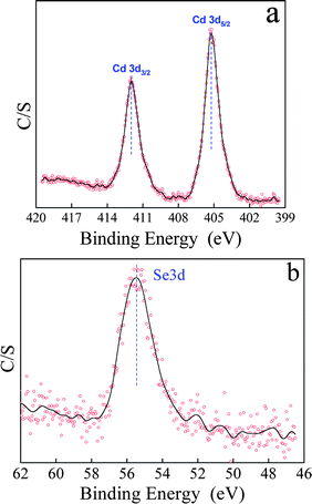 | ||
| Fig. 2 XPS patterns of the hollow CdSe nanospheres: (a) Cd 3d5/2 and (b) Se 3d. | ||
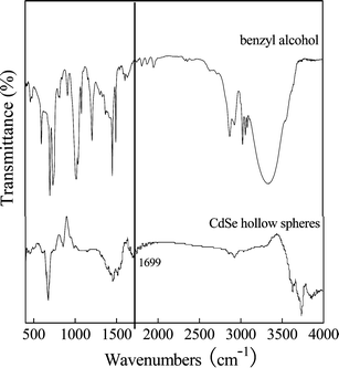 | ||
| Fig. 3 IR spectra of the hollow CdSe nanospheres and benzyl alcohol. | ||
An overview scanning electron microscopy (SEM) image at low magnification (Fig. 4a) illustrates that the sample consists entirely of relatively uniform nanospheres with an average diameter of about 100 nm, without the presence of broken spheres. The hollow structure was further confirmed by a transmission electron microscopy (TEM) image (Fig. 4b), in which the hollow inner and thicker outer shell can clearly be seen. The high resolution TEM image recorded of a shell (Fig. 4c) displays an evident contrast, but with different lattice fringes in the overall view. This result indicates that, on the one hand, the shell of the hollow nanospheres consist of highly crystalline nanocrystals, but on the other, that these small nanocrystals aggregate together in a non-oriented attachment that is similar to what is observed in the synthesis of other metal oxide nanocrystals.20–22 The selected area electron diffraction (SAED) pattern shown in Fig. 4d further confirms the polycrystalline nature of the hollow nanospheres.
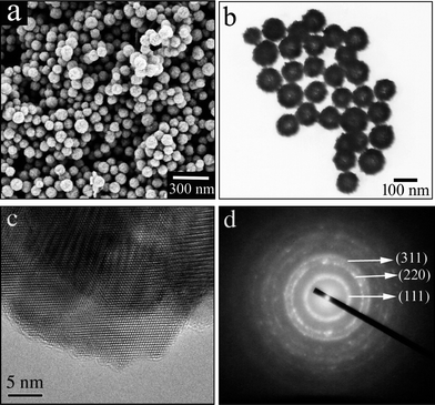 | ||
| Fig. 4 (a) SEM, (b) TEM, (c) HRTEM and (d) SAED patterns of the obtained hollow CdSe nanospheres. | ||
To further confirm the formation mechanism of this hollow structure, time-dependent experiments were performed. With a short reaction time (4 h, Fig. 5a), the crystallite aggregates, which consist of nanoclusters, give an irregular morphology. When the reaction time is prolonged (8 h, Fig. 5b), relatively uniform nanospheres were observed. With further prolonging of the reaction time (24 h, Fig. 5c), the nanospheres undergo a hollowing process, and the hollow interior starts to emerge. The solid evacuation is pronounced after 36 h of reactive aging (Fig. 4b), during which time these nanospheres do not change much in size but become more uniform. This observation provides direct evidence that the formation of CdSe hollow nanospheres is related to Ostwald ripening, which is similar to the formation of hollow anatase TiO2 nanospheres reported by Zeng.23
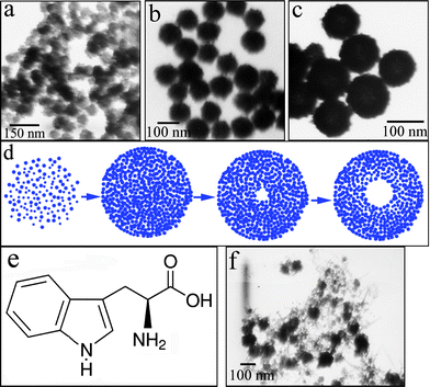 | ||
| Fig. 5 The evolution of CdSe nanostructures with reaction time: (a) 4, (b) 8 and (c) 24 h; (d) an illustration of the formation process of the CdSe hollow nanospheres based on Ostwald ripening; (e) the structure of tryptophan; (f) a TEM image of the CdSe product obtained without tryptophan. | ||
Fig. 5d illustrates the whole morphology evolution process based on Ostwald ripening. On the basis of this mechanism, numerous small crystallites first nucleate under solvothermal conditions and then gradually aggregate into spheres to minimize their surface energies by an oriented attachment, which was further confirmed by the above HRTEM measurement. Subsequently, via Ostwald ripening, the central cavity is created, accompanied by the growth of larger outer crystallites at the expense of inner ones. In the present case, tryptophan, with a rich coordination chemistry (Fig. 5e),24 plays a crucial role in the formation of the hollow structure. This was confirmed by a tryptophan-free experiment, where irregular nanoparticles instead of hollow ones were formed, as shown in Fig. 5f. Therefore, it could be reasonably deduced that after the tryptophan is introduced into reaction system, a Cd-tryptophan complex forms. Under solvothermal conditions, the complex not only restrains nucleation but also restrains the growth of the particles. Simultaneously, the tryptophan may also serve as a capping agent to prevent particles from agglomerating. This process induces a decrease of particle size compared with the case without adding tryptophan, resulting in the formation of the central cavity via Ostwald ripening. This Ostwald ripening process is symmetric, while the group of Papadimitrakopoulos25 previously reported an asymmetric Ostwald ripening of CdSe dots to rods. Our unique CdSe hollow structures may bring with them novel properties and applications.
These hollow CdSe nanospheres exhibited a substantially enhanced microwave absorption compared with the CdSe sample obtained in the absence of tryptophan (denoted as solid) no matter what the sample thickness. The reflection loss (RL) of CdSe/paraffin with 70 wt% CdSe was calculated using the relative complex permeability and permittivity at a given frequency and thickness layer according to the transmit-line theory, which is summarized as the following equations:26–29
| RL(dB) = 20log|(Zin − Z0)/(Zin + Z0)| | (1) |
 | (2) |
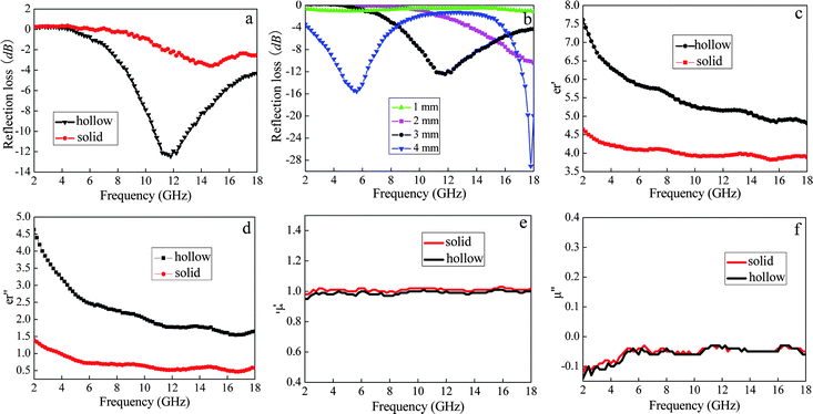 | ||
| Fig. 6 (a) Reflection loss of hollow and solid CdSe nanostructures vs. frequency. (b) Reflection loss of hollow samples with different thicknesses. The frequency dependence of the (c) real and (d) imaginary parts of complex permittivity. The frequency dependence of the (e) real and (f) imaginary parts of permeability. | ||
When the thickness was 2 mm, the minimum RL reached less than −10 dB at more than 18 GHz, while two peaks (5.6 GHz, −16 dB and 17.8 GHz, 31 dB) were observed with a thickness of 4 mm. The reflection loss difference between the hollow and solid CdSe nanostructures is largely related to their size effects, i.e., whether the size of the building blocks, consisting of CdSe nanostructures, is large or small. To investigate the possible mechanism of the enhancement of microwave absorption by hollow structures, the complex relative permittivity and permeability of the samples was independently measured. As we know, the real parts of the relative complex permittivity and permeability symbolize their storage ability for electromagnetic energy, while the imaginary parts represent their ability to loose it.30Fig. 6c–6f show the real and imaginary parts of the complex relative permittivity and permeability measured for both hollow and solid samples. It can be clearly seen that ε″ is positive, while μ″ is negative over the whole measured frequency range for both samples, suggesting that the CdSe sample is a dielectric loss material. Moreover, we can see that both the real and imaginary parts of the relative permittivity for the hollow sample are higher than those for the solid sample, indicating that the hollow CdSe nanostructures have a higher electrical conductivity than the solid ones. The higher electric conductivity of the hollow sample may be due to the small size of its building blocks, consisting of hollow structures.
Therefore, based on the above results, it can be concluded that the enhanced microwave absorption properties of the hollow sample result from its small size effect.
4. Conclusions
In summary, we have reported a synthesis of hollow CdSe nanospheres by a ligand-assisted solvothermal method. The hollow structures consist of small nanocrystallite building blocks that endow them with a higher electrical conductivity and accordingly results in enhanced microwave absorption properties. These hollow structures potentially hold promise as microwave absorbers for military electronics radio frequency interference.Acknowledgements
This work was supported by the Natural Science Foundation of China (NSFC, nos. 20731002, 10876002, 20771022, 91022006 and 20973023), the 111 Project (B07012), the Program for New Century Excellent Talents in University, the Open Fund of State Key Laboratory of Explosion Science and Technology and Beijing Institute of Technology (no. ZDKT08-01 and YBKT09-13), the Specialized Research Fund for the Doctoral Program of Higher Education (SRFDP, no. 200800070015), the Funding Project for Science and Technology Program of Beijing Municipal Commission (no. Z09010300820902) and the Key Foundation of China Academy of Engineering Physics (no. 2009A0302017).References
- Y. D. Yin, R. M. Rioux, C. K. Erdonmez, S. Hughes, G. A. Somorjai and A. P. Alivisatos, Science, 2004, 304, 711 CrossRef CAS.
- Q. Peng, Y. Dong and Y. Li, Angew. Chem., Int. Ed., 2003, 42, 3027 CrossRef CAS.
- Y. Sun, B. Mayers and Y. Xia, Adv. Mater., 2003, 15, 641 CrossRef CAS.
- F. Caruso, R. A. Caruso and H. Mohwald, Science, 1998, 282, 1111 CrossRef CAS.
- M. E. Davis, Nature, 2002, 417, 813 CrossRef CAS.
- S. W. Kim, M. Kim, W. Y. Lee and T. Hyeon, J. Am. Chem. Soc., 2002, 124, 7642 CrossRef CAS.
- C. I. Zoldesi and A. Imhof, Adv. Mater., 2005, 17, 924 CrossRef CAS.
- H. P. Liang, H. M. Zhang, J. S. Hu, Y. G. Guo, L. J. Wan and C. L. Bai, Angew. Chem., Int. Ed., 2004, 43, 1540 CrossRef CAS.
- J. Gao, B. Zhang, X. Zhang and B. Xu, Angew. Chem., Int. Ed., 2006, 45, 1220 CrossRef CAS.
- R. L. Penn and J. F. Banfield, Science, 1998, 281, 969 CrossRef CAS.
- W. Z. Ostwald, Phys. Chem., 1900, 34, 495.
- B. Liu and H. C. Zeng, Small, 2005, 1, 566 CrossRef CAS.
- J. Li and H. C. Zeng, Angew. Chem., Int. Ed., 2005, 44, 4342 CrossRef CAS.
- A. L. Washington II and G. F. Strouse, J. Am. Chem. Soc., 2008, 130, 8916 CrossRef CAS.
- J. Huang, D. Stockwell, Z. Q. Huang, D. L. Mohler and T. Q. Lian, J. Am. Chem. Soc., 2008, 130, 5632 CrossRef CAS.
- L. J. Deng and M. G. Han, Appl. Phys. Lett., 2007, 91, 023119 CrossRef.
- C. Wang, X. J. Han, P. Xu, J. Y. Wang, Y. C. Du, X. H. Wang, W. Qin and T. Zhang, J. Phys. Chem. C, 2010, 114, 3196 CrossRef CAS.
- S. H. Wu and D. H. Chen, J. Colloid Interface Sci., 2003, 259, 282 CrossRef CAS.
- (a) P. Xu, X. J. Han, C. Wang, D. H. Zhou, Z. S. Lv, A. H. Wen, X. H. Wang and B. Zhang, J. Phys. Chem. B, 2008, 112, 10443 CrossRef CAS; (b) Y. L. Yan, Y. Li and X. F. Qian, Mater. Sci. Eng., B, 2003, 103, 202 CrossRef; (c) Q. Peng, Y. J. Dong, Z. X. Deng and Y. D. Li, Inorg. Chem., 2002, 41, 5249 CrossRef CAS.
- D. Zitoun, N. Pinna, N. Frolet and C. Belin, J. Am. Chem. Soc., 2005, 127, 15034 CrossRef CAS.
- W. K. Koh, A. C. Bartnik, F. W. Wise and C. B. Murray, J. Am. Chem. Soc., 2010, 132, 3909 CrossRef CAS.
- C. O'Sullivan, R. D. Gunning, A. Sanyal, C. A. Barrett, H. Geaney, F. R. Laffir, S. Ahmed and K. M. Ryan, J. Am. Chem. Soc., 2009, 131, 12250 CrossRef CAS.
- J. Li and H. C. Zeng, J. Am. Chem. Soc., 2007, 129, 15839 CrossRef CAS.
- G. W. Gokel and M. M. Daschbach, Coord. Chem. Rev., 2008, 252, 886 CrossRef CAS.
- R. F. Li, Z. T. Luo and F. Papadimitrakopoulos, J. Am. Chem. Soc., 2006, 128, 6280 CrossRef CAS.
- M. Matsumoto and Y. Miyata, IEEE Trans. Magn., 1997, 33, 4459 CrossRef.
- P. Singh, V. K. Babbara, A. Razdan, R. K. Puri and T. C. Goel, J. Appl. Phys., 2000, 87, 4362 CrossRef CAS.
- T. Maeda, S. Sugimoto and T. Kagotani, J. Magn. Magn. Mater., 2004, 284, 113 CrossRef CAS.
- X. Han and Y. Wang, Phys. Scr., 2007, t129, 335 CrossRef CAS.
- C. Wang, X. J. Han, P. Xu, J. Y. Wang, Y. C. Du, X. H. Wang, W. Qin and T. Zhang, J. Phys. Chem. C, 2010, 114, 3196 CrossRef CAS.
| This journal is © The Royal Society of Chemistry 2010 |