Self-aligned nanolithography by selective polymer dissolution†
Huijuan
Zhang
abc,
Chee-Leong
Wong
b,
Yufeng
Hao
b,
Rui
Wang
b,
Xiaogang
Liu
ad,
Francesco
Stellacci
ae and
John T. L.
Thong
*ab
aAdvanced Materials for Micro- and Nano-Systems Program, Singapore-MIT Alliance, 4 Engineering Drive 3, Singapore
bCentre for IC Failure Analysis and Reliability, Department of Electrical and Computer Engineering, National University of Singapore, 4 Engineering Drive 3, Singapore. E-mail: elettl@nus.edu.sg; Fax: +65 6779 1103; Tel: +65 6516 2270
cInstitute of Microelectronics, A*STAR (Agency for Science, Technology and Research), 11 Science Park Road, Singapore Science Park II, Singapore
dDepartment of Chemistry, National University of Singapore, 3 Science Drive 3, Singapore
eDepartment of Materials Science and Engineering, Massachusetts Institute of Technology, Cambridge, Massachusetts, USA
First published on 9th September 2010
Abstract
We report a novel approach to the fabrication of self-aligned nanoscale trench structures in a thin polymer layer covering on conductive materials. By passing AC current through a polymer-coated nanowire in the presence of an appropriate solvent, a self-aligned nanotrench is formed in the polymer overlayer as a result of accelerated dissolution while the rest of the device remains covered. Similar results have been achieved for polymer-coated graphene ribbons. Such polymer-protected devices in which only the active component is exposed should find important applications as electrical sensors in aqueous solutions, particularly in cases where parasitic ionic currents often obscure sensing signals.
Introduction
There is great interest in the development of nanoscale biosensors, motivated by the capability of integrating nanostructured optical and electrical materials with current semiconductor technology for highly sensitive and ultrafast detection.1 Conventional electronic biosensors utilize surface interactions with biomolecules in aqueous solution, to affect the electrical properties of the active sensor element that converts the bio-event into an electrical signal.2 As the detection is invariably carried out in solution, there is a need to avoid parasitic ionic currents through parallel conduction paths between the electrodes exposed to the liquid. In particular, for solutions of high ionic strength, such ionic currents often substantially mask the biodetection signal.3 One of the methods identified to work around this problem is to selectively create only a small opening structure at the sensing part for attachment of biological probes, while keeping exposed electrodes electrically insulated. The challenge lies in the fabrication of such devices where a nanoscale sensing component, such as a nano-gap or a semiconductor nanowire, has to be fabricated underneath an insulating layer (e.g. a polymer coating) and in registry with a small opening that exposes the sensor to the solution containing the analyte. At the same time, it is desirable that the fabrication process should be facile and inexpensive.A wide range of approaches have been reported for high-resolution patterning of protective polymer materials in the past decades.4 Apart from conventional lithography approaches that require pattern registration and alignment, other reported techniques include the use of electric-field and Joule heating to locally ablate the polymer in self-aligned processes.5 Another interesting approach involves modifying the surface morphology of polymeric resists by using atomic force microscopy (AFM) based electrostatic nanolithography in which perturbations or depressions can be created in polymer films.6 In this article, we report an on-chip self-aligned method in which an opening structure is formed by differential dissolution of a polymer film covering a conductive nanowire or a graphene ribbon by Joule heating. For potential device applications, we also demonstrate the selective deposition of nanoparticles on the exposed nanowire as well as self-aligned patterning of an opening on the graphene ribbon.
Results and discussion
Method
The process flow of the self-aligned patterning method is illustrated in Scheme 1. Lines of ∼250 nm in width and 20 µm in length were patterned on a 500 nm thick SiO2 coated Si substrate by electron beam lithography (EBL). Chromium/gold (5/40 nm) metal electrodes were deposited by thermal evaporation on the patterned samples, followed by a lift-off process (Scheme 1a). The sample was then spin-coated with 80 nm thick polymethylmethacrylate (PMMA, 950k molecular weight) (Scheme 1b). Subsequently, the sample was immersed in p-xylene solution, and AC current was applied to the metallic nanowire to induce Joule heating which in turn heats the overlying PMMA (Scheme 1c). AC current was used to prevent electromigration in the Au nanowire as the current density (∼108 A cm−2) required to attain a sufficiently high temperature approaches typical values for the onset of electromigration under DC current stressing.7 Upon dissolution, a self-aligned nanotrench forms in the vicinity of the nanowire by differential dissolution, while the rest of the device remains polymer-protected (Scheme 1d).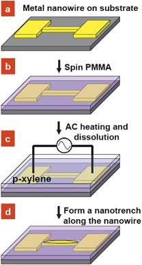 | ||
| Scheme 1 Schematic process flow: (a) patterning of a metal nanowire with contact pads by EBL on a Si substrate, (b) deposition of a PMMA layer on the substrate, (c) selective dissolution of the polymer layer by AC current heating in the presence of p-xylene solvent and (d) formation of a self-aligned nanotrench structure along the nanowire. | ||
Solvent selection
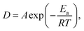
It is well-known that polymer dissolution rate is markedly dependent on temperature.8 By applying current to a polymer-coated pre-patterned conductive nanostructure, localized Joule heating can cause a temperature rise in the overlying polymer layer. The elevated temperature results in a fast dissolution of the polymer in the hot region, leading to the formation of a well-defined pattern. An appropriate solvent needs to satisfy three criteria: (1) the dissolution rate of PMMA in the solvent should be negligible at room temperature; (2) the solvent should dissolve PMMA quickly at temperatures above room temperature, i.e., a sharp increase in dissolution rate with temperature is desirable; (3) the solvent needs to be non-polar and non-ionic. Several solvents were tested for their dissolution rates at elevated temperatures compared to room temperature in order to select an appropriate candidate for nanotrench fabrication. Methyl isobutyl ketone (MIBK) was found to dissolve PMMA too rapidly as it dissolves a 600 nm thick film in less than one minute at room temperature. MIBK was then diluted with isopropyl alcohol (IPA) which slowed the dissolution. However, it was found that during electrical heating, dissolution occurred in a fast and uncontrollable manner (Fig. S1 in ESI†). Since IPA and MIBK are both polar solvents and slightly ionic, the presence of an electric field accelerates the dissolution of the PMMA during the dissolution process.9 For ionic solvents, conduction-assisted carrier drift and material transfer may also occur.10 Benzene, a non-polar solvent, also did not provide a satisfactory differential rate of dissolution. It dissolves a PMMA film at about 5 nm s−1 at room temperature, which is too fast for differential dissolution to achieve reasonable patterns. Finally, p-xylene (C8H10) was chosen as the non-polar solvent that prevents the electric-field-accelerated dissolution and also has a preferred dissolution rate.Characterization of dissolution rate
Characterization of PMMA dissolution in p-xylene was conducted by dissolving PMMA films of pre-coated samples at temperatures ranging from 298 K to 348 K for various durations while recording the average dissolution rate as shown in Fig. 1a. The thickness of PMMA on each coated sample before dissolution was measured by using a FILMETRICS F20 thin film measurement system. After dissolution of the PMMA for different duration time t at temperature T in p-xylene, the PMMA thickness was subsequently measured. The average dissolution rate D at different T was then obtained by calculating the dissolved thickness over the known duration time t. Fig. 1a shows that the dissolution rate D scales nearly exponentially with temperature aswhere A is a constant, Ea is the activation energy, R is the gas constant, and T is the temperature. A straight line fit on an Arrhenius plot (Fig. 1b) is obtained and yields an activation energy of 132 kJ mol−1, which is comparable to the value, 105 kJ mol−1, reported by Cooper and coworkers for PMMA dissolution in 2-butanone.8 The difference in the activation energy could be attributed to the use of polar rather than non-polar solvents in the reported work. Hence, p-xylene is a good solvent for the system as the dissolution rate is negligible (<1 nm s−1) at room temperature and rises rapidly at higher temperatures, thereby providing a practical working window for experiments to be carried out.
 | ||
| Fig. 1 (a) PMMA dissolution rate in p-xylene as a function of temperature and (b) the corresponding Arrhenius plot. | ||
Selective dissolution
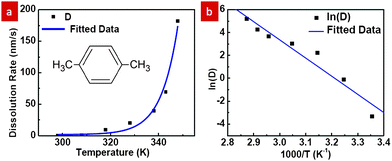
As a proof-of-concept experiment, we have successfully fabricated a self-aligned nanotrench structure in a polymer layer along a pre-patterned Au nanowire while the rest of the device remains protected by the polymer. Fig. 2a shows a typical Scanning Electron Microscopy (SEM) image of a 252 nm wide nanowire prior to selective dissolution. The nanowire was spin-coated with a thin PMMA layer of ∼80 nm thickness. After AC current heating and dissolution, a nanotrench that is well aligned to the nanowire was formed, as shown in Fig. 2b. It is believed that the nanowire was fully exposed after dissolution as supported by the line profiles shown in Fig. 2c and d. The applied heating power determines the local temperature and hence the dissolution rate and dissolved thickness for a given period. Experiments show that a typical heating power of ∼0.01 W is needed to create a nanotrench with 5 s dissolution time. It is noted that the dissolved pattern has dimensions in the order of 1 micrometre, which is considerably larger than the nanowire dimension, ∼250 nm in width. The enlargement of dissolved pattern dimension is due to the effect of thermal diffusion during heating and the dissolution of the polymer heated up around the nanowire.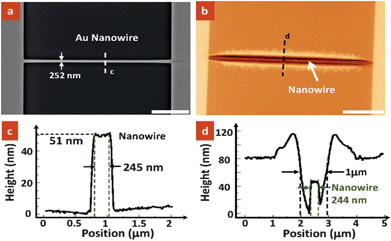 | ||
| Fig. 2 (a) SEM image of a gold nanowire obtained. (b) Atomic Force Microscopy (AFM) topographic image showing the formation of nanotrench on the nanowire after selective polymer dissolution Scale bars for (a) and (b) = 5 µm. (c and d) The corresponding height profiles along lines (c) and (d) indicated in (a) and (b), respectively. As observed, the width of the nanowire is measured to be ∼244 nm, which is consistent with the recoded value in the SEM image and the measured data in the AFM image, indicating the full dissolution of the PMMA layer on the nanowire. | ||
The nanowire served as a line source and generated isotherms of cylindrical distribution with a finite diameter.11 To illustrate the thermal distribution around the nanowire during the dissolution process, the temperature profile was simulated using the multi-physics simulation software ANSYS 10.0 as shown in Fig. 3a. It took less than 1 µs for the device in p-xylene to achieve a steady-state temperature profile, and hence it is reasonable to equate the dissolution time with the heating time. It is observed that the heat was confined between the nanowire and electrode pads (blue: room temperature). Fig. 3b and c show the simulated temperature profile along (x-direction) and across (y-direction) the nanowire. While the opening at the trench closely correlates with the isotherm dimension of the order of 1 micrometre, the PMMA profile around the nanowire does not follow exactly (Fig. S2 in ESI†). The sloped sidewalls of the polymer arise from the dissolution process from top to bottom with the polymer below having a shorter dissolution interaction with the solvent. Dissolution rate D is obtained as a function of position across the nanowire. Since the heating and dissolution time is 5 s in our experimental work, the dissolved thickness vs. the position across the nanowire was derived and plotted in Fig. 3d. It is clearly seen that the resulting depth profile matches the nanotrench pattern shown in Fig. 2b with a width of about 1 µm. However, instead of obtaining smooth edges at the trench opening as simulated in Fig. 3d, an ∼30 nm hump is observed experimentally shown in Fig. 2b. It is known that for dissolution to occur, solvent must first diffuse into the polymer film to form a rubbery surface layer.12 The polymer then can undergo a transformation from a solid film to solid-swollen layer to a gel layer followed by liquid layer before being dissolved into the solvent.12 The small expansion along the nanotrench edge is possibly due to the swelling process and polymer redistribution during dissolution.
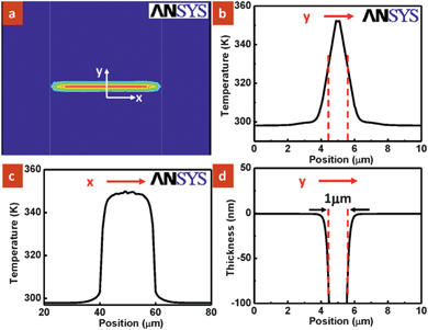 | ||
| Fig. 3 (a) Simulated temperature profile of the PMMA surface showing isotherms. The blue and red colors indicate cold and hot regions of the polymer, respectively. (b and c) Respective temperature plot as a function of position on the PMMA surface as indicated by y and x direction shown in (a). (d) Calculated thickness of the polymer dissolved vs. position across the nanowire (y-axis). | ||
To confirm the removal of the PMMA polymer at the site of the self-aligned nanotrench, we have demonstrated site-specific assembly of Au nanoparticles onto the exposed nanowire. The nanotrench device was first modified with a capturing DNA strand (5′HS–C6A10). A solution of Au nanoparticles (∼15 nm) modified with a complementary DNA strand (5′HS–C6T10) was then added to the device (Fig. 4a).13 To avoid charging artifacts when examining the nanowire by SEM, the PMMA layer was removed by low power oxygen plasma. As anticipated, upon DNA hybridization Au nanoparticles were selectively assembled on the exposed nanowire (Fig. 4b). Control experiments were carried out to exclude the possibility of non-specific binding of Au nanoparticles to the surface as shown in Fig. S3 (ESI†). In addition, the full exposure of nanowire is also supported by an electrical conduction experiment as illustrated in Fig. 4c. A droplet of test solution (0.3 M NaCl) was applied onto the device surface. The IV characteristics of the setup were measured in a probe station, by inserting one probe into the electrolyte and the other probe contacting one of the bond pads attached to the nanowire. This test is to measure the ionic current from the nanowire. Measurements were taken before (i.e., the nanowire protected by PMMA) and after (i.e., the nanowire exposed upon removal of the polymer at the nanowire site) the selective polymer dissolution. As observed (Fig. 4b), the ionic current through the nanowire after the dissolution is apparent after polymer dissolution, whereas negligible current flowed prior to dissolution.
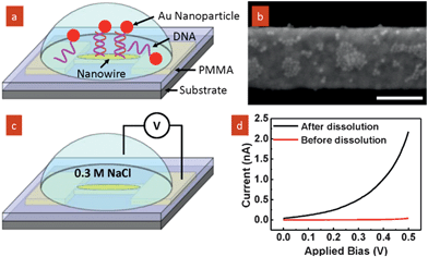 | ||
| Fig. 4 (a) Schematic of self-assembly of Au nanoparticles by DNA hybridization; (b) SEM image showing selective assembly of nanoparticles onto the exposed nanowire. Scale bar is 200 nm. (c) Schematic of electrical conduction measurements of the device before and after selective polymer dissolution in test solution (0.3 M NaCl). (d) IV characteristics measured before and after polymer dissolution. | ||
Another promising application of our self-aligned nanolithography technique is to selectively expose polymer protected graphene devices. A piece of multi-layer graphene (∼10 µm × 100 µm in size) was prepared by mechanical exfoliation. Electrode leads were patterned on the graphene by EBL and metallized by evaporation. The device was further coated with PMMA and examined by an optical microscope as shown in Fig. 5a. Fig. 5b shows the optical image after site-specific dissolution of the PMMA. By applying a heating power of ∼0.01 W to the graphene between the electrodes labeled as 1 and 2, a self-aligned opening was obtained on the graphene while the rest of the graphene sheet remained protected. An AFM topographic profile of the as-fabricated trench structure marked by the dotted line shown in Fig. 5b clearly shows the removal of the PMMA layer. The formation of small humps at the trench opening site is also consistent with that observed when using the nanowire as the conducting material. The technique demonstrated here is particularly important for developing solution-gated graphene field effect transistors as the source and drain electrodes can be protected by the PMMA layer from direct contact with the gate electrolyte.14 Significantly, as shown in Fig. 5b, this patterning method allows site-specific modification or functionalization of the graphene.
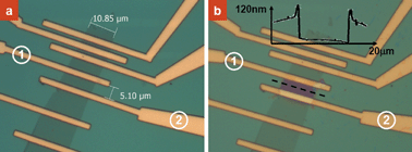 | ||
| Fig. 5 Optical images of PMMA-coated a graphene device before (a) and after (b) selective dissolution of the polymer. The inset in (b) is the AFM height profile of the pattern marked by the dotted line. | ||
Conclusion
In summary, we have developed a novel method for self-aligned exposure of polymer-protected nanostructures or graphene sheets. The polymer layer is preferentially dissolved as a result of localized Joule heating of the nanostructure. The exposed nanostructures have been utilized for site-specific immobilization of Au nanoparticles. Importantly, the polymer layer prevents the device from direct contact with any analyte solution while leaving only the nanowire accessible. Furthermore, we have demonstrated the selective opening of holes on polymer-coated graphene, which yields an attractive device for various sensing applications.15 It is conceivable that this selective dissolution approach can be generalized to other systems with thermoplastic polymers as the protective layer and various conductive nanowires (or nanotubes) as the active device element. Once refined, the approach should be particularly useful for developing sensors for biological detection with significantly reduced signal interference caused by background ionic current.Experimental
Fabrication of self-aligned nanotrench on nanowire
950k molecular weight PMMA (3% in chlorobenzene), supplied by MicroChem Corp., was spun on a 500 nm thick SiO2 coated Si substrate at 6000 rpm for one minute followed by baking at 120 °C for 15 min. Nanowires with interconnecting electrodes were then patterned by electron beam lithography. Cr (5 nm, as an adhesion layer) and Au (40 nm) were deposited using thermal evaporation (BOC Edwards, Auto 306 Vacuum Evaporator) on the patterned samples followed by a lift-off process by soaking in acetone for 30 min to create Au nanowires. This was followed by optical lithography using AZ5212 photoresist to define large bond pads (400 µm × 400 µm). A second layer of 100 nm thick Au and 10 nm Cr was thermally evaporated and lifted-off to deposit the contact pads. The sample was then spun with 2% PMMA at 6000 rpm for one minute followed by baking at 120 °C for 15 min. Next, the nanowire was bonded to external electrical connections. Sinusoidal AC current with an amplitude typically to 10 mA at 1 MHz (typical power input ∼0.01 W) was used to heat the nanowire. The dissolution was carried out in p-xylene for 5 s. The sample was finally dried by nitrogen flow.Temperature simulation
The structure used was a four-layer model, consisting of the solvent layer (50 µm thickness), PMMA (80 nm thickness), the nanowire/electrode layer (40 nm thickness) and silicon oxide (500 nm thickness). The actual experimental values were used as parameters for the simulation as follows: current amplitude = 10 mA, length of the nanowire = 20 µm and resistance of the nanowire = 120 Ω.Functionalization of Au nanowires and Au nanoparticles
All oligonucleotides were purchased from Sigma Aldrich Ltd. 15 nm diameter Au nanoparticle solution was prepared following a method in the literature.16 The 5′-terminal disulfide of oligonucleotides strands was first cleaved by dithiothreitol (DTT) in a buffer solution (0.1 M phosphate, pH 8.0) for 2 hours, and purified with a NAP-5 column purchased from GE Healthcare Ltd. The Au colloid solution was then mixed with the purified thiol–DNA solution and left overnight. The concentration was gradually increased to 0.3 M NaCl, 10 mM NaH2PO4/Na2HPO4, pH 7 buffer (0.3 M PBS buffer) every 4 hours. After 48 hours, the nanoparticles were centrifuged and re-dispersed in 0.3 M PBS buffer. The surface modification of the nanowire with thiolated oligonucleotides was carried out via a similar procedure. For Au nanoparticle assembly, the nanowire substrate immersed into the solution of Au nanoparticles (2 nM) was incubated at 80 °C and slowly cooled down for DNA hybridization. The sample was then extensively rinsed using 0.3 M PBS buffer solution to avoid trapping of nanoparticle solution in the trench and finally blow-dried by nitrogen flow.Acknowledgements
This work is supported by Singapore-MIT Alliance, National University of Singapore, and A*STAR (SERC Grant 062 101 0023). H. Zhang is grateful to the Singapore-MIT Alliance for support through a fellowship.Notes and references
- (a) I. Hyungsoon, X.-J. Huang, B. Gu and Y.-K. Choi, Nat. Nanotechnol., 2007, 2, 430–434 CrossRef; (b) W. Chen, Z. S. Lu and C. M. Li, Anal. Chem., 2008, 80, 8485–8492 CrossRef CAS; (c) W. H. Hu, Z. S. Lu, Y. S. Liu and C. M. Li, Langmuir, 2010, 26, 8386–8391 CrossRef CAS; (d) P. E. Sheehan and L. J. Whitman, Nano Lett., 2005, 5, 803–807 CrossRef CAS; (e) S.-J. Park, T. A. Taton and C. A. Mirkin, Science, 2002, 295, 1503–1506 CrossRef CAS; (f) A. J. Haes and R. P. Van Duyne, J. Am. Chem. Soc., 2002, 124, 10596–10604 CrossRef CAS; (g) F. Wang and X. Liu, Chem. Soc. Rev., 2009, 38, 976–989 RSC; (h) F. Wang, Y. Han, C. S. Lim, Y. Lu, J. Wang, J. Xu, H. Chen, C. Zhang, M. Hong and X. Liu, Nature, 2010, 463, 1061–1065 CrossRef CAS; (i) J. N. Anker, W. P. Hall, O. Lyandres, N. C. Shah, J. Zhao and R. P. Van Duyne, Nat. Mater., 2008, 7, 442–453 CrossRef CAS; (j) T. G. Drummond, M. G. Hill and J. K. Barton, Nat. Biotechnol., 2003, 21, 1192–1199 CrossRef CAS; (k) F. Wang, D. Banerjee, Y. Liu, X. Chen and X. Liu, Analyst, 2010, 135, 1839–1854 RSC.
- (a) M. Yang, J. Wang, H. Li, J.-G. Zheng and N. N. Wu, Nanotechnology, 2008, 19, 75502 CrossRef; (b) B. Y. Lee, S. M. Seo, D. J. Lee, M. Lee, J. Lee, J.-H. Cheon, E. Cho, H. Lee, I.-Y. Chung, Y. J. Park, S. Kim and S. Hong, Lab Chip, 2010, 10, 894–898 RSC; (c) B. Xu, P. Zhang, X. Li and N. Tao, Nano Lett., 2004, 4, 1105–1108 CrossRef CAS.
- S. Seo, M. D. King, R. F. Young, L. B. Kish and M. Cheng, Microelectron. Eng., 2008, 85, 1484–1489 CrossRef CAS.
- (a) A. Majumdar, P. I. Oden, J. P. Carrejo, L. A. Nagahara, J. J. Graham and J. Alexander, Appl. Phys. Lett., 1992, 61, 2293–2295 CrossRef CAS; (b) M. J. Lercel, H. G. Craighead, A. N. Parikh, K. Seshadri and D. L. Allara, Appl. Phys. Lett., 1996, 68, 1504–1506 CrossRef CAS; (c) X. Liu, S. Guo and C. A. Mirkin, Angew. Chem., Int. Ed., 2003, 42, 4785–4788 CrossRef CAS; (d) X. Liu, Y. Zhang, D. K. Goswami, J. S. Okasinski, K. Salaita, P. Sun, M. J. Bedzyk and C. A. Mirkin, Science, 2005, 307, 1763–1766 CrossRef CAS; (e) Z. Nie and E. Kumacheva, Nat. Mater., 2008, 7, 277–290 CrossRef CAS; (f) X. Zhou, Y. Chen, B. Li, G. Lu, F. Y. C. Boey, J. Ma and H. Zhang, Small, 2008, 4, 1324–1328 CrossRef CAS.
- (a) Y. C. Lin, J. Bai and Y. Huang, Nano Lett., 2009, 6, 2234–2238 CrossRef; (b) I. Park, Z. Li, A. P. Pisano and R. S. Williams, Nano Lett., 2007, 7, 3106–3111 CrossRef CAS; (c) H. Zhang, R. J. Barsotti, C.-L. Wong, X. Xue, X. Liu, F. Stellacci and J. T. L. Thong, Small, 2009, 5, 2797–2801 CrossRef CAS.
- (a) S. F. Lyuksyutov, P. B. Paramonov, R. A. Sharipov and G. Sigalov, Phys. Rev. B: Condens. Matter Mater. Phys., 2004, 70, 174110 CrossRef; (b) S. F. Lyuksyutov, R. A. Vaia, P. B. Paramonov, S. Juhl, L. Waterhouse, R. M. Ralich, G. Sigalov and E. Sancaktar, Nat. Mater., 2003, 2, 468–472 CrossRef CAS.
- J. Tao, N. W. Cheung and C. Hu, IEEE Electron Device Lett., 1993, 14, 554–556 CrossRef CAS.
- W. J. Cooper, P. D. Krasicky and F. Rodriguez, J. Appl. Polym. Sci., 1986, 31, 65–73 CrossRef CAS.
- S. Takatoshi, Adv. Colloid Interface Sci., 1997, 71, 281–287.
- X. N. Xie, H. J. Chung, C. H. Sow, A. A. Bettiol and A. T. S. Wee, Adv. Mater., 2005, 17, 1386–1390 CrossRef CAS.
- D. Poulikakos, Conduction Heat Transfer, Prentice Hall, 1994, pp. 337–339 Search PubMed.
- B. A. Miller-Chou and J. L. Koenig, Prog. Polym. Sci., 2003, 28, 1223–1270 CrossRef CAS.
- (a) X. Xue, F. Wang and X. Liu, J. Am. Chem. Soc., 2008, 130, 3244–3245 CrossRef CAS; (b) W. Xu, X. Xue, T. Li, H. Zeng and X. Liu, Angew. Chem., Int. Ed., 2009, 48, 6849–6852 CrossRef CAS; (c) X. Xue, W. Xu, F. Wang and X. Liu, J. Am. Chem. Soc., 2009, 131, 11668–11669 CrossRef CAS.
- (a) P. K. Ang, S. Wang, Q. Bao, J. T. L. Thong and K. P. Loh, ACS Nano, 2009, 3, 3587–3594 CrossRef CAS; (b) S. Wang, P. K. Ang, Z. Wang, A. L. L. Tang, J. T. L. Thong and K. P. Loh, Nano Lett., 2010, 10, 92–98 CrossRef CAS.
- (a) V. Dua, S. P. Surwade, S. Ammu, S. R. Agnihotra, S. Jain, K. E. Roberts, S. Park, R. S. Ruoff and S. K. Manohar, Angew. Chem., Int. Ed., 2010, 49, 2154–2157 CrossRef CAS; (b) J. D. Fowler, M. J. Allen, V. C. Tung, Y. Yang, R. B. Kaner and B. H. Weiller, ACS Nano, 2009, 3, 301–306 CrossRef CAS; (c) F. Schedin, A. K. Geim, S. V. Morozov, E. W. Hill, P. Blake, M. I. Katsnelson and K. S. Novoselov, Nat. Mater., 2007, 6, 652–655 CrossRef CAS.
- J. J. Storhoff, R. Elghanian, R. C. Mucic, C. A. Mirkin and R. L. Letsinger, J. Am. Chem. Soc., 1998, 120, 1959–1964 CrossRef CAS.
Footnote |
| † Electronic supplementary information (ESI) available: Uncontrollable dissolved pattern of PMMA after dissolution in polar solvent, the PMMA profile around the nanowire and control experiments of nanopariticle assembly. See DOI: 10.1039/c0nr00398k |
| This journal is © The Royal Society of Chemistry 2010 |