Nanoelectronic biosensors based on CVD grown graphene†
Yinxi
Huang‡
a,
Xiaochen
Dong‡
ab,
Yumeng
Shi
b,
Chang Ming
Li
a,
Lain-Jong
Li
*b and
Peng
Chen
*a
aSchool of Chemical and Biomedical Engineering, Nanyang Technological University, Singapore 637457. E-mail: chenpeng@ntu.edu.sg
bSchool of Materials Science and Engineering, Nanyang Technological University, Singapore 639798. E-mail: ljli@ntu.edu.sg
First published on 11th June 2010
Abstract
Graphene, a single-atom-thick and two-dimensional carbon material, has attracted great attention recently. Because of its unique electrical, physical, and optical properties, graphene has great potential to be a novel alternative to carbon nanotubes in biosensing. We demonstrate the use of large-sized CVD grown graphene films configured as field-effect transistors for real-time biomolecular sensing. Glucose or glutamate molecules were detected by the conductance change of the graphene transistor as the molecules are oxidized by the specific redox enzyme (glucose oxidase or glutamic dehydrogenase) functionalized onto the graphene film. This study indicates that graphene is a promising candidate for the development of real-time nanoelectronic biosensors.
1. Introduction
Single-walled carbon nanotubes (SWNTs), which are crystalline carbon sheets rolled into long cylindrical tubes with diameters of 1–2 nm, have attracted much attention in the development of novel nanoelectronic biosensors owing to their exceptional electrical properties.1–3 The applications of SWNTs, however, are often plagued with several problems. In particular, it is difficult to separate metallic nanotubes from semiconducting ones, and when single or only a few SWNTs are used, it is challenging to manipulate them for device fabrication, and they are too small to interface with large-sized bio-species (e.g., cells or tissues) and to be readily bio-functionalized. The flat relative of SWNT, graphene, has been discovered recently.4 In contrast to the one-dimensional structured SWNT, graphene is a one-atom-thick two-dimensional carbon sheet. As it exhibits unique structural and electrical properties (e.g. high carrier mobility and bipolar field-effect characteristics), graphene has been anticipated to be a novel, better alternative to carbon nanotubes in various applications5–8 including biosensor development.9–13 Graphene based biosensors are advantageous in terms of, for example, large detection area, possibilities of new sensing mechanisms, and ease of effective functionalization. In this study, redox enzyme-modified CVD-grown graphene devices for real-time detection of glucose and glutamate are demonstrated.2. Experimental section
2.1 Preparation of graphene film
Large-sized graphene films with single-layered and few-layered domains were grown on a Ni film (∼500 nm thick, evaporated on SiO2/Si wafer) at ∼1000 °C by chemical vapor deposition (CVD) of carbon using a mixture of methane and hydrogen as the carbon source. As-grown graphene film on Ni film was spin-coated with poly(methyl methacrylate) (PMMA) dissolved in chlorobenzene, followed by baking at 120 °C for 20 min. The Ni film underneath the graphene film was etched away by HCl solution (HCl![[thin space (1/6-em)]](https://www.rsc.org/images/entities/char_2009.gif) :H2O = 1:10) over a period of 8 h to release the PMMA/graphene film into the solution. The PMMA/graphene film was then picked up by a quartz substrate. After dried in air, a small amount of liquid PMMA/chlorobenzene solution was dropped onto the PMMA/graphene film to dissolve the precoated PMMA. At last, the PMMA/graphene film was immersed into acetone to remove PMMA, followed by annealing at 450 °C for 20 min (hydrogen/argon atmosphere) to remove the residual PMMA.
:H2O = 1:10) over a period of 8 h to release the PMMA/graphene film into the solution. The PMMA/graphene film was then picked up by a quartz substrate. After dried in air, a small amount of liquid PMMA/chlorobenzene solution was dropped onto the PMMA/graphene film to dissolve the precoated PMMA. At last, the PMMA/graphene film was immersed into acetone to remove PMMA, followed by annealing at 450 °C for 20 min (hydrogen/argon atmosphere) to remove the residual PMMA.
2.2 Functionalization of GOD and GluD
A graphene device was incubated with a 5 mM linker molecule (1-pyrenebutanoic acid succinimidyl ester, i-DNA Biotechnology) in dimethylformamide (DMF) for 2 h at room temperature, and washed with pure DMF and deionized (DI) water. The linker-modified graphene was then incubated with 10 mg mL−1 glucose oxidase (GOD, Sigma-Aldrich) or 2 mg mL−1 glutamic dehydrogenase (GluD, Sigma-Aldrich) in Na2CO3-NaHCO3 buffer solution (pH 9.0) overnight at 4 °C followed by rinsing with DI water and phosphate buffered saline solution (PBS). To deactivate and block the excess reactive groups remaining on the surface, the device was incubated with 0.1 M ethanolamine solution (pH 9.0) for 30 min and then rinsed by DI water.2.3 Electrical measurements
All measurements were conducted using a semiconductor device analyzer (Agilent, B1500A), and carried out while the graphene devices were biased at 100 mV. The gating voltage was applied via an Ag/AgCl electrode in the PBS solution (10 mM, pH 7.2). In the biosensing experiments, the current between source and drain (Ids) of graphene FET was continuously monitored at a gate voltage, Vg = 0 V.3. Results and discussion
Large-sized graphene films with single-layered and few-layered domains were grown by chemical vapor deposition. Source and drain electrodes were prepared at the two opposite edges of the graphene film (∼2 × 4 mm2) using silver paint and silicone rubber was used to insulate the two electrodes and define a solution/recording chamber between the electrodes. Fig. 1A shows a typical optical image of the CVD growth graphene film. The grown films are heterogeneous with dominating single layered area (50–60%) and few layered islands. The number of graphene layers can be revealed by Raman spectroscopy with excitation wavelength at 488 nm (Fig. 1B). Regions indicated by a, b, c, and d in Fig. 1A are identified as single-, double-, triple- and multiple-layered by their characteristic intensity ratio of the 2D Raman peak at ∼2700 cm−1 to G peak at ∼1582 cm−1 (∼3.4, ∼1.0, ∼0.78, and ∼0.25, respectively).14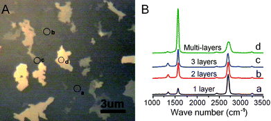 | ||
| Fig. 1 (A) Typical optical image of the CVD growth graphene film, consisting of single-layered domains (dark area) and few-layered domains (bright areas). (B) Raman spectra of several regions on the graphene film (indicated as a, b, c, d in both panel A and panel B, see text for definition). The number of graphene layers can be determined by the peak intensity ratio of 2D and G bands in the Raman spectrum. | ||
Glucose oxidase (GOD) or glutamic dehydrogenase (GluD) was immobilized onto graphene film via a linker molecule (1-pyrenebutanoic acid succinimidyl ester) which on one end firmly attaches to the graphene surface through π–π interaction with a pyrene group and on the other end covalently reacts with the amino group on the enzyme by an amide bond (Fig. 2A). As shown by the AFM images of graphene film before and after functionalization (Fig. S1†), the immobilization of enzymes is effective with good coverage. The transfer curves, i.e., the current between source and drain (Ids) of the graphene field-effect transistor (FET) biased at Vds = 100 mV versus the liquid-gate voltage (Vg) applied via an Ag/AgCl electrode immersed in the PBS solution (10 mM, pH 7.2) bathing the graphene film, were measured on the bare graphene device, the device conjugated with the linker, and the device after functionalization of GOD or GluD (Fig. S2†). The alterations in the transfer curve indicate the success of the functionalization steps and both GOD and GluD functionalized devices exhibit similar bipolar field-effect characteristics. The hole mobilities of the GOD and GluD functionalized devices in Fig. S2† are ∼520 cm2 V−1 S−1 and ∼630 cm2 V−1 S−1, respectively. In the biosensing experiments, graphene FET operated at the p-type region as the solution voltage Vg was held at 0 V, and its Ids was continuously monitored with Vds = 100 mV using a semiconductor device analyzer (Agilent, B1500A).
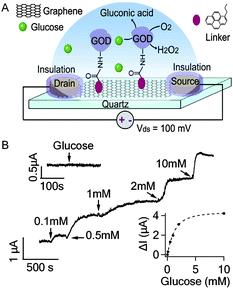 | ||
| Fig. 2 (A) Schematic illustration of GOD functionalized graphene FET. (B) Current responses to the addition of glucose to various concentrations. The upper inset shows that GOD free graphene FET is not responsive to 10 mM glucose. The lower inset shows the response curve of the graphene FET to glucose fitted by an exponential function. | ||
GOD catalyzes the oxidation of glucose in the following reaction: β-D-glucose + O2 + H2O → D-glucono-1,5-lactone + H2O2. In a typical experiment shown in Fig. 2B, obvious increase of Ids was observed when glucose in PBS buffer was added to the recording chamber initially filled with 300 μL PBS solution to reach the final concentration of 0.1 mM. In addition, Ids increased further as more glucose was added to reach higher concentrations. As shown in the lower inset of Fig. 2B, the graphene response tends to saturate at glucose concentrations > 10 mM, perhaps partly due to the limited density of GODs on the graphene film and/or the limited reaction rate of GOD. The percentage increase in the graphene conductance in response to 0.1 mM glucose was 0.76 ± 0.16% (n = 3 devices), which was significantly higher than the noise level 0.07 ± 0.01%. Our observations are consistent with the previous experiment using single-SWNT based field-effect transistors (FETs)15 which, however, showed lower sensitivity. For comparison, we have conducted similar experiments using GOD functionalized thin-film FETs based on SWNT network (also a two dimensional nanocarbon substrate, ∼8 mm2 in size, Fig. S3†)16,17 and found that the conductance of SWNT network also increased upon addition of glucose. However, the detection sensitivity (>1 mM) is lower than the graphene FETs (Fig. S4A†). The percentage increase in the SWNT network conductance in response to 5 mM glucose was only 0.24 ± 0.14% (n = 3 devices). In the control experiment (upper inset in Fig. 2B), glucose (10 mM) was not able to cause appreciable responses from GOD free graphene sensors (only with the linker molecules and ethanolamine passivation), suggesting that the current responses to glucose observed in GOD functionalized devices are due to the enzymatic activities of GODs. Furthermore, GOD functionalized graphene FETs are not responsive to glutamate and common interferences including L-ascorbic acid, uric acid and acetaminophen (data not shown), indicating that our graphene based nanoelectronic biosensor can specifically detect glucose.
Glutamate is a major neurotransmitter secreted by neurons in the central nervous system. GluD oxidizes glutamate in the following reaction: L-glutamate + β-NAD + H2O ↔ α-ketoglutarate + β-NADH + NH4+. In order to facilitate the oxidation reaction, 5 mM β-NAD (Sigma-Aldrich) was added to the recording chamber before addition of glutamate. As shown in Fig. 3, a low concentration of glutamate (5 μM) caused a clear current increase in graphene device. The response of the graphene device displayed two linear detection ranges: from 5 to 50 μM and from 50 μM to 1.2 mM, respectively (lower inset, Fig. 3). The percentage increase in the graphene conductance in response to 5 μM glutamate was 0.35 ± 0.08% (n = 3 devices), much higher than the noise level. As control, glutamate (1 mM) did not lead to any signal from GluD free graphene sensors (upper inset, Fig. 3). The addition of glucose and interference molecules (L-ascorbic acid, uric acid and acetaminophen) did not cause an obvious response (data not shown). These results show that the GluD-modified graphene device can specifically detect glutamate with low detection limit and wide range, mediated by the enzymatic activities of GluD. In contrast, GluD functionalized SWNT network responded to addition of glutamate inconsistently and with small signal amplitude (Fig. S4B†).
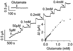 | ||
| Fig. 3 Current responses of GluD functionalized graphene FET to the addition of glutamate to various concentrations. The upper inset shows that GluD free graphene FET is not responsive to 1 mM glutamate. The lower inset shows the response curve of the graphene FET to glutamate with two fitting lines indicating the two linear response regions. | ||
Catalytic oxidation of both glucose and glutamate led to increase in graphene conductance. Such increase is not because of direct transfer of electrons generated from the oxidative reaction to the graphene which would decrease graphene conductance and cause negative shift of the Dirac (minimum conductance) point of the transfer curve in contrast to our observations (Fig. 1, 2 and 4). The transfer curves in Fig. 4 demonstrate that the device conductance (at Vg = 0) increased in both cases, consistent with the Ids–time measurement shown in Fig. 1B and 2. The addition of glutamate obviously right-shifted the transfer curve (Fig. 4B), indicating the p-doping effect. On the other hand, the addition of glucose only caused slight right-shift (expanded transfer curve shown in the inset of Fig. 4A). Such small p-doping effect may explain the lower detection sensitivity for glucose as compared to that of glutamate. It is likely that the products from the oxidative reaction are responsible for the increase of graphene conductance. As shown in Fig. 5, H2O2 and NH4OH produced from glucose and glutamate oxidation respectively can indeed induce increase in graphene conductance, while D-glucono-1,5-lactone (the other oxidation product of glucose) and α-ketoglutarate (another oxidation product of glutamate) cannot cause any conductance change.
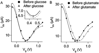 | ||
| Fig. 4 (A) Transfer curves before and after adding glucose (10 mM) to the GOD functionalized graphene FET. (B) Transfer curves before and after adding glutamate (1 mM) to the GluD functionalized graphene FET in the presence of 5 mM β-NAD. | ||
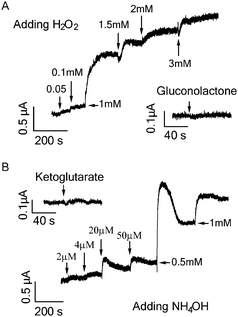 | ||
| Fig. 5 (A) Current responses of graphene FET to addition of products from glucose oxidation: H2O2 and D-glucono-1,5-lactone (1 mM). (B) Current responses of graphene FET to addition of products of glutamate oxidation: NH4OH and α-ketoglutarate (1 mM). | ||
The detection limits of our graphene based glucose sensor (0.1 mM) and glutamate sensor (5 μM) are comparable to the commonly used electrochemical sensors,17,18 yet inferior to some state-of-the-art electrochemical sensors integrated with functional nanomaterials.19,20 However, as the techniques to fabricate high-performance graphene FETs are rapidly evolving, it is anticipated that the ability of graphene based biomolecular sensors would be significantly advanced in the near future. It appears that graphene sensors are superior to SWNT-network sensors. This may be attributable to several reasons: (1) the sensitivity of SWNT network is impaired by the presence of metallic tubes; (2) the functionalization of enzymes is more effective and uniform on flat graphene film than on small nanotubes; and (3) the functionalization steps may alter the tube-to-tube contact in the SWNT network or lead to loss of some nanotubes.
4. Conclusions
In summary, we demonstrate nanoelectronic biosensors based on large-sized CVD grown graphene film functionalized with specific redox mediators for detection of glucose and glutamate. This study postulates the promising potentials of graphene in nanoelectronic biosensing. In addition, given its perfect 2D structure, exceptional electronic properties, and the ability to support cell adhesion and growth,21 graphene devices promise applications in interfacing with living cells and detecting dynamic bimolecular secretion and other activities from them.22,23Acknowledgements
This work is supported by an A-Star SERC grant (# 072 101 0020) and a grant from National Research Foundation (NRF-CRP-07-2).References
- P. Avouris, Acc. Chem. Res., 2002, 35, 1026 CrossRef CAS.
- B. L. Allen, P. D. Kichambare and A. Star, Adv. Mater., 2007, 19, 1439 CrossRef CAS.
- Y. X. Huang and P. Chen, Adv. Mater., 2010 DOI:10.1002/adma.200904235.
- A. K. Geim and K. S. Novoselov, Nat. Mater., 2007, 6, 183 CrossRef CAS.
- X. C. Dong, D. L. Fu, W. J. Fang, Y. M. Shi, P. Chen and L. J. Li, Small, 2009, 5, 1422 CrossRef CAS.
- F. Schedin, A. K. Geim, S. V. Morozov, E. W. Hill, P. Blake, M. I. Katsnelson and K. S. Novoselov, Nat. Mater., 2007, 6, 652 CrossRef CAS.
- J. T. Robinson, F. K. Perkins, E. S. Snow, Z. Q. Wei and P. E. Sheehan, Nano Lett., 2008, 8, 3137 CrossRef CAS.
- J. D. Fowler, M. J. Allen, V. C. Tung, Y. Yang, R. B. Kaner and B. H. Weiller, ACS Nano, 2009, 3, 301 CrossRef CAS.
- N. Mohanty and V. Berry, Nano Lett., 2008, 8, 4469 CrossRef CAS.
- C. H. Lu, H. H. Yang, C. L. Zhu, X. Chen and G. N. Chen, Angew. Chem., Int. Ed., 2009, 48, 4785 CrossRef CAS.
- Y. Ohno, K. Maehashi, Y. Yamashiro and K. Matsumoto, Nano Lett., 2009, 9, 3318 CrossRef CAS.
- X. C. Dong, Y. M. Shi, W. Huang, P. Chen and L. J. Li, Adv. Mater., 2010, 22, 1649 CrossRef CAS.
- S. J. He, B. Song, D. Li, C. F. Zhu, W. P. Qi, Y. Q. Wen, L. H. Wang, S. P. Song, H. P. Fang and C. H. Fan, Adv. Funct. Mater., 2010, 20, 453 CrossRef.
- A. Reina, X. T. Jia, J. Ho, D. Nezich, H. B. Son, V. Bulovic, M. S. Dresselhaus and J. Kong, Nano Lett., 2009, 9, 30 CrossRef CAS.
- K. Besteman, J. O. Lee, F. G. M. Wiertz, H. A. Heering and C. Dekker, Nano Lett., 2003, 3, 727 CrossRef CAS.
- J. Zhang, D. L. Fu, M. B. Chan-Park, L. J. Li and P. Chen, Adv. Mater., 2009, 21, 790 CrossRef CAS.
- Y. X. Huang, W. J. Zhang, H. Xiao and G. X. Li, Biosens. Bioelectron., 2005, 21, 817 CrossRef CAS.
- S. Chakrabortya and C. R. Raj, Electrochem. Commun., 2007, 9, 1323 CrossRef.
- U. Yogeswaran and S. M. Chen, Sensors, 2008, 8, 290 CrossRef CAS.
- L. H. Tang, Y. H. Zhu, L. H. Xu, X. L. Yang and C. Z. Li, Talanta, 2007, 73, 438 CrossRef CAS.
- S. Agarwal, X. Z. Zhou, F. Ye, Q. Y. He, G. C. K. Chen, J. C. Soo, F. Boey, H. Zhang and P. Chen, Langmuir, 2010, 26, 2244 CrossRef CAS.
- Y. X. Huang, H. G. Sudibya, D. L. Fu, R. H. Xue, X. C. Dong, L. J. Li and P. Chen, Biosens. Bioelectron., 2009, 24, 2716 CrossRef CAS.
- H. G. Sudibya, J. M. Ma, X. C. Dong, S. Ng, L. J. Li, X. W. Liu and P. Chen, Angew. Chem., Int. Ed., 2009, 48, 2723 CrossRef CAS.
Footnotes |
| † Electronic supplementary information (ESI) available: AFM images of graphene film before and after functionalization, transfer curves of graphene after every step, SEM image of CNT-net, and detection results using CNT-net devices. See DOI: 10.1039/c0nr00142b |
| ‡ These authors contributed equally to the work. |
| This journal is © The Royal Society of Chemistry 2010 |