Facile synthesis of IV–VI SnS nanocrystals with shape and size control: Nanoparticles, nanoflowers and amorphous nanosheets†
Jiajia
Ning
ab,
Kangkang
Men
a,
Guanjun
Xiao
a,
Li
Wang
b,
Quanqin
Dai
a,
Bo
Zou
*a,
Bingbing
Liu
a and
Guangtian
Zou
a
aState Kay Laboratory of Superhard Materials, Jilin University, Changchun, 130012, P. R. China. E-mail: zoubo@jlu.edu.cn
bDepartment of Materials Science and Engineering, Jilin University, Changchun, 130012, P. R. China
First published on 3rd July 2010
Abstract
SnS nanocrystals have been synthesized in a simple and facile way. Sn6O4(OH)4 is introduced to synthesize tin sulfide, which is used as tin precursor. By changing the reaction conditions (reaction temperature and Sn/S molar ratio), SnS nanocrystals with different shape and size can be produced. SnS nanoparticles and nanoflowers with orthorhombic crystal structure have uniform size distribution. The SnS nanoflowers firstly transform to polycrystalline nanoflowers, and then become amorphous nanosheets. The drive force of amorphization reduces the high free-energy of nanocrystals. The layered crystal structure of SnS is the main reason for the shape evolution and amorphization processes. The optical properties of nanoparticles are investigated by optical absorption spectra. The optical direct band gap and optical indirect band gap in SnS nanoparticles are 3.6 eV and 1.6 eV, respectively. Compared to direct band gap (1.3 eV) and indirect band gap (1.09 eV) in bulk SnS, both direct transition and indirect transition in nanoparticles show an obvious quantum-size effect.
Introduction
As narrow band gap semiconductors, IV–VI series semiconductors are a research hotspot in nanoscience and nanotechnology. Much effort has been paid to the synthesis and application of IV–VI series semiconductors, such as PbS, PbSe, PbTe and SnTe.1 They can be widely used in photovoltaics, near-infrared detectors, biomedical applications, electrochemical, thermoelectric and solar cells,2 because their band gap can cover all the near-infrared region. However, the toxicity of Pb has limited their application in many fields. Synthesis of new, nontoxic and low-cost narrow band-gap semiconductor nanocrystals by a simple approach has attracted the attention of many scientists. Low toxic IV–VI tin chalcogenides are a good choice for narrow band gap semiconductors. However, synthesis of tin chalcogenide nanocrystals with uniform size-distribution, high crystallinity and good optical properties is an open problem in synthetic chemistry.Tin sulfide (SnS) is an important IV–VI series semiconductor; bulk SnS has a direct band gap at 1.3 eV and an indirect band gap at 1.09 eV.3 Because of its orthorhombic structure and band gap region, low toxicity and low cost, SnS can be used in near-infrared detectors and photovoltaic materials.4 SnS also has potential in solar cells and photoconductors because of its similar direct band gap to silicon and its high conductivity and absorption coefficient.3 Based on the effects of the morphology and size on properties, SnS nanocrystals could exhibit different properties from those in bulk material. Compared to these semiconductors with cubic crystal structures (CdS, CdSe and PbS), the layered crystal structure of tin sulfide causes many difficulties in the synthesis of nanocrystals with a small enough size and uniform size distribution. Until now, only Alexander Eychmüller et al. and Richard D. Tilley et al. have synthesized SnS nanoparticles of small size (smaller than 10 nm),5 although a few reports on the synthesis of SnS nanocrystals have been published.6 However, expensive and toxic Sn[N(SiMe3)2]2 was used as an Sn source to synthesize SnS nanoparticles.1e,5a
Herein, we report a simple and facile way to synthesize SnS nanoparticles and nanoflowers with smaller size, uniform size distribution and high crystallinity; single crystalline nanoflowers transform to amorphous SnS nanosheets. Simple tin oxide hydroxide (Sn6O4(OH)4) was dissolved in oleic acid (OA) and oleylamine (OLA) as the tin precursor, and then the thioacetamide/OLA was injected to the tin precursor. The synthetic route of Sn6O4(OH)4 has been developed in previous reports.7 The solution became dark red as soon as we injected thioacetamide/oleylamine to the precursor solution. After a few minutes, the dark red solution was quenched to room temperature. The evolution from single crystalline nanoflowers to amorphous nanosheets is explained. The as-prepared SnS nanoparticles exhibit an obvious quantum-size effect in direct and indirect transition.
Experimental
Materials
SnCl2 (98%), 1-octadecene (ODE, 90%) and oleic acid (OA, 90%) were purchased from Aldrich. Oleylamine (OLA, ≥70%) was purchased from Fluka. Thioacetamide (99.0%) was purchased from Tianjing Tiantai Chemical Company. Toluene, chloroform, ethanol and methanol were purchased from Beijing Chemical Company. All chemicals were used in the experiments without further purification.Synthesis section
All of the experiments were carried out using standard airless techniques: a vacuum/dry nitrogen gas Schlenk line was used for synthesis and a nitrogen glove-box for storing and handling air- and moisture-sensitive chemicals. Thioacetamide/OLA solution (0.1 mmol ml−1) was prepared in a glove-box by dissolving thioacetamide in OLA at room temperature.An equal volume of methanol was added to the solution and nanocrystals were collected by centrifuging. These nanocrystals were purified three times. Finally, the nanocrystals were dissolved in nonpolar solvents, forming stable concentrated colloidal solutions.
Characterization
Transmission electron microscopy (TEM) images were obtained in a Hitachi H-8100IV transmission electron microscopy using an acceleration voltage of 200 kV. High resolution transmission electron microscopy (HRTEM) images were taken at a JEOL JEM-2100 at 200kV, and point-to-point resolution of this HRTEM is 0.19 nm. Powder X-ray diffraction (XRD) was obtained on a Bruker D8 diffractometer operating at 40 kV and 40 mA, using Cu-Kα target. Data were collected from 15° to 80° with a sampling interval 0.02° per step and a counting rate of 0.2 s per step. Ultraviolet–visible absorption (UV-vis-NIR) spectra were measured by a Shimadzu UV-3150 spectrometer; the nanocrystals were dispersed in toluene. Photoluminescence (PL) of SnS nanocrystals was taken at Photon Technology International photoluminescence equipment.Result and discussion
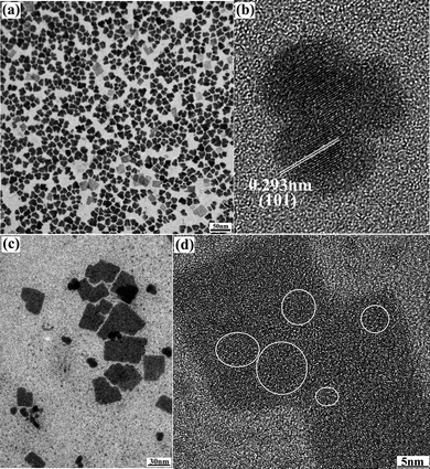
At different reaction temperature and Sn/S molar ratio, SnS nanocrystals are obtained with various morphologies and sizes. The shape and size of the samples are characterized by transmission electron microscopy (TEM) and high resolution transmission electron microscopy (HRTEM). When the Sn/S molar ratio is 1![[thin space (1/6-em)]](https://www.rsc.org/images/entities/char_2009.gif) :1 and the temperature is 150 °C, SnS nanoparticles are produced (Fig. 1). The diameter of SnS nanoparticles is about 5 nm with uniform size distribution. The standard deviation of SnS nanoparticles is only 3%, the SnS nanoparticles are monodisperse as shown in histogram (Fig. 3). Fig. 1b gives HRTEM images of SnS nanoparticles, the high crystallinity of SnS nanoparticles and lattice of nanoparticles can be clearly observed. Every SnS nanoparticles are single crystalline in nature. Fig. 1c shows HRTEM images of one SnS nanoparticles, the interplanar distance of 0.293 nm agrees with (101) lattice fringe of orthorhombic SnS. SAED images of Fig. 1c have the characterization of single crystalline, which agrees with the result of HRTEM images.
:1 and the temperature is 150 °C, SnS nanoparticles are produced (Fig. 1). The diameter of SnS nanoparticles is about 5 nm with uniform size distribution. The standard deviation of SnS nanoparticles is only 3%, the SnS nanoparticles are monodisperse as shown in histogram (Fig. 3). Fig. 1b gives HRTEM images of SnS nanoparticles, the high crystallinity of SnS nanoparticles and lattice of nanoparticles can be clearly observed. Every SnS nanoparticles are single crystalline in nature. Fig. 1c shows HRTEM images of one SnS nanoparticles, the interplanar distance of 0.293 nm agrees with (101) lattice fringe of orthorhombic SnS. SAED images of Fig. 1c have the characterization of single crystalline, which agrees with the result of HRTEM images.
 | ||
| Fig. 1 Transmission electron microscopy (TEM) images (a), high resolution transmission electron microscopy (HRTEM) images (b and c) and SAED images (d) of SnS nanoparticles, which were synthesized with an Sn/S = 1:1 (molar ratio) at 150 °C. | ||
When the temperature of injecting thioacetamide/OLA is 120 °C and the Sn/S molar ratio is 2:1, the products are SnS nanoflowers and nanosheets (Fig. 2). The TEM images of products taken at 3 min are shown in Fig. 2a. The shape of nanocrystals is nanoflowers with the size of 13 nm. The size distribution is uniform and the standard deviation is 6% (the histogram in Fig. 3). HTREM images show that the nanoflowers with an irregular shape are single crystalline nanoparticles (Fig. 2b). The interplanar distance in nanoflowers is same as in nanoparticles; 0.293 nm which accords with the plane distance of (101) in orthorhombic SnS. The crystal structure of nanoflowers is orthorhombic SnS. In the reaction, the products taken at longer reaction time are nanosheets, as shown in Fig. 2c. The size of the nanosheets is from 40 nm to 100 nm, and they are square in shape. Most of the area in the HRTEM images of nanosheets is amorphous, and the crystal lattice could be seen only in few fields, as labelled in Fig. 2d. The nanosheets are amorphous. In the reaction, the previous products are nanoflowers, and then all the nanoflowers are transformed to amorphous nanosheets. The amorphization process is included in the shape evolution from nanoflowers to nanosheets.
 | ||
| Fig. 2 Transmission electron microscopy (TEM) images of SnS nanoflowers (a), HRTEM images of SnS nanoflowers (b), TEM images of SnS nanosheets (c) and HRTEM images of SnS nanosheets (d). | ||
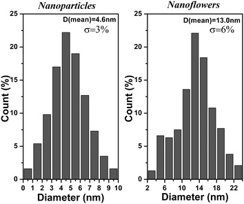 | ||
| Fig. 3 The histograms of size distribution of SnS nanoparticles and SnS nanoflowers. | ||
By changing the reaction conditions, SnS nanocrystals with various morphologies can be achieved. When the temperature of the injected S source is 120 °C, nanoparticles with a size of 15 nm are obtained with an Sn/S molar ratio of 1:1 (Fig. S1a).† With an Sn/S molar ratio of 1:2, nanoparticles with a size of 7 nm appear (Fig. S1b).† When the temperature is 150 °C, we get nanoparticles and nanocubes with different Sn/S molar ratios. The size and shape of nanoparticles with an Sn/S molar ratio of 2:1 similar to nanoparticles obtained at 1:1. Cubic-like nanoparticles appear when the molar ratio of Sn/S is 1:2. The phase structure of all samples is confirmed by powder X-ray diffraction, as shown in Fig. S2.† This sample XRD pattern of characteristic of an herzenbergite structure, which is similar to previous results on SnS nanocrystals.6 This orthorhombic SnS accords to JCPDS no. 39-0354 with a = 4.329 Å, b = 11.19 Å and c = 3.98 Å. In Fig. S2,† all the diffraction peaks could be indexed to orthorhombic SnS. The lower intensity and broader width of these diffraction peaks indicate the smaller size of SnS nanocrystals. XRD patterns of nanosheets are also given in Fig. S3.† No obvious diffraction peaks can be observed, indicating that the SnS nanosheets are amorphous. Both HRTEM and XRD illustrate that the amorphization process occurs in the transition from nanoflowers to nanosheets.
Fig. 4 gives the process and scheme of transition from nanoflowers to nanosheets. From Fig. 2b, we know that the nanoflowers are single crystalline. After a few minutes, the nanoflowers transform to amorphous nanosheets. TEM images give a mixture of polycrystalline nanoflowers and amorphous nanosheets (Fig. 4b). Single crystalline SnS nanoflowers gradually transform to amorphous nanosheets by oriented attachment; the polycrystalline nanoflowers are intermediate (Fig. 4). Coupled with the oriented attachment of nanoflowers to nanosheets, the amorphization process is included. We think the layered crystal structure of SnS is the main reason for the shape evolution and amorphization process. The layered crystal structure induces many difficulties in the synthesis of 0-dimensional (0D) or 3-dimensional (3D) nanocrystals with a smaller size and uniform size distribution.5 For layered crystal structure semiconductor nanocrystals, 0D or 3D nanocrystals are a metastable state, which has the tendency to transform to more-stable 2-dimensional (2D) nanosheets. 2D nanosheets are the normal shape for semiconductor nanocrystals with a layered crystal structure.6 Moreover, amorphization is normal in many research fields, as high pressure can induce amorphization in many materials.8 High pressure supplies enough energy to destroy the chemical bonds in the crystalline material and overcome the barrier to the amorphous state. So, if the supplied energy is sufficient to overcome the barrier or the barrier to amorphous state is small enough, the amorphization process could easily be observed. In SnS nanoflowers, the layered crystal structure induces a smaller barrier to the amorphous state, so amorphization can be observed in the shape evolution from SnS nanoflowers to nanosheets. Furthermore, we calculated the Gibbs free energy for SnS nanoflowers and SnS nanosheets. The Gibbs free energy for nanoflowers and nanosheets can be expressed as GNFs and GNSs, respectively. ΔG is the change of Gibbs free energy in the shape evolution from nanoflowers to nanosheets, as shown in Fig. 5. E1 is the barrier from SnS nanoflowers to SnS nanosheets. At low reaction temperatures, the produced nanocrystalline material would have many defects because of the low crystal temperature.9 These defects would induce the high free energy in nanocrystalline material, which may be higher than the free energy in amorphous material. If ΔG is smaller than zero, the transition from defective nanoflowers to amorphous nanosheets is reasonable, and the transformation between the two crystallinity states would happen only if the supplied energy is sufficient to overcome the barrier, E1. By thermodynamics theory, the Gibbs free energy at the solution state is used as reference; we can get ΔG < 0 (further detailed discussion is listed the ESI†). So, the shape evolution from defective nanoflowers to amorphous nanosheets is favourable thermodynamically, and the driving force of this transition reduces the free energy of the nanocrystals. The defective nanoflowers with high free energy are unstable and tend to a more stable state, amorphous nanosheets. The temperature can provide enough energy to overcome the barrier to amorphous, E1.
 | ||
| Fig. 4 TEM images of transition from SnS nanoflowers to nanosheets and the scheme of transition. | ||
 | ||
| Fig. 5 Scheme of nanocrystals free energy at different crystalline states. | ||
Optical properties are important to semiconductors. By tuning the size of the nanocrystals, a quantum-size effect can be exhibited, which could be widely used in near-infrared detectors, photoconductors and photovoltaic materials. Much attention has been paid to the synthesis of SnS nanocrystals by tuning their optical properties.5,6Fig. 6 gives the UV-vis-NIR optical absorption spectra of SnS nanoparticles; the spectra show a continuous absorption near the UV-vis region. To get the relation of the energy (Eg) and the type of optical transition responsible for optical absorption, the absorption spectra can be analyzed by the following equation for near-edge absorption:10
| (αhv)n = B(hv − Eg) | (1) |
 | ||
| Fig. 6 UV-vis-NIR absorption spectra of SnS nanoparticles. | ||
 | ||
| Fig. 7 The dependence of (αhν)1/2 on photon energy (hν) and (αhν)2 on photon energy (hν) of SnS nanoparticles. | ||
Conclusions
SnS nanocrystals with various shapes and size have been synthesized. Tin oxide hydroxide (Sn6O4(OH)4) is introduced to synthesis of SnS nanocrystals, which provides a new tin precursor for the synthesis of tin sulfide and improves the synthetic chemistry in tin chalcogenides. Nanoparticles and nanoflowers are single-crystalline and have a uniform size distribution. With prolonged reaction times, SnS nanoflowers aggregate to amorphous nanosheets. The driving force of amorphization is the reduction of the high free energy of nanoflowers and this transition is thermodynamically favourable. UV-vis-NIR absorption spectra are used to investigate the properties of SnS nanocrystals. SnS nanoparticles show obvious quantum-size effects in direct transition and indirect transition of SnS nanoparticles. Study of the optical properties of SnS nanocrystals will expand the applications of SnS nanocrystals. We think this work will promote the study of the synthesis and properties of SnS nanocrystals, and the successful synthesis of SnS nanocrystals will provide an important reference to other layered crystal structure nanocrystals.Acknowledgements
This work was supported by NSFC (Nos. 20773043, and 10979001), the National Basic Research Program of China (No. 2005CB724400 and No. 2007CB808000).Notes and references
- (a) M. A. Hines and G. D. Scholes, Adv. Mater., 2003, 15, 1844 CrossRef CAS; (b) C. B. Murray, S. Sun, W. Gaschler, H. Doyle, T. A. Betley and C. R. Kagan, IBM J. Res. Dev., 2001, 45, 47 CrossRef CAS; (c) J. E. Murphy, M. C. Beard, R. J. Elligson and A. Nozik, J. Am. Chem. Soc., 2006, 128, 3241 CrossRef CAS; (d) J. J. Urban, D. V. Talapin, E. V. Shevchenko and C. B. Murray, J. Am. Chem. Soc., 2006, 128, 3248 CrossRef CAS; (e) M. V. Kovalenko, W. Heiss, E. V. Shevchenko, J. S. Lee, H. Schwinghammer, A. P. Alivisatos and D. V. Talapin, J. Am. Chem. Soc., 2007, 129, 11354 CrossRef CAS.
- (a) R. D. Schaller, M. A. Petruska and V. I. Klimov, J. Phys. Chem. B, 2003, 107, 13765 CrossRef CAS; (b) M. S. Neo, N. Venkatram, G. S. Li, W. S. Chin and J. Wei, J. Phys. Chem. C, 2009, 113, 19055 CrossRef CAS; (c) D. V. Talapin and C. B. Murray, Science, 2005, 310, 86 CrossRef CAS; (d) M. S. Dresselhaus, G. Chen, M. Y. Tang, R. Yang, H. Lee, D. Wang, Z. Ren, J. P. Fleurial and P. Gogna, Adv. Mater., 2007, 19, 1043 CrossRef CAS; (e) S. L. Mao, J. J. Zhao, S. Y. Zhang, H. L. Niu, B. K. Jin and Y. P. Tian, J. Phys. Chem. C, 2009, 113, 18091 CrossRef CAS.
- J. B. Johnson, H. Jones, B. S. Latham, J. D. Parker, R. D. Engelken and C. Barber, Semicond. Sci. Technol., 1999, 14, 501 CrossRef CAS.
- (a) A. Ghazali, Z. Zainal, M. Z. Hussein and A. Kassim, Sol. Energy Mater. Sol. Cells, 1998, 55, 237 CrossRef CAS; (b) N. K. Reddy and K. T. R. Reddy, Thin Solid Films, 1998, 325, 4 CrossRef; (c) J. P. Singh and R. K. Bedi, Thin Solid Films, 1991, 199, 9 CrossRef CAS.
- (a) S. G. Hickey, C. Waurisch, B. Rellinghaus and A. Eychmüller, J. Am. Chem. Soc., 2008, 130, 14978 CrossRef CAS; (b) Y. Xu, N. Al-Salim, C. W. Bumby and R. D. Tilley, J. Am. Chem. Soc., 2009, 131, 15990 CrossRef CAS.
- (a) S. Schlecht and L. Kienle, Inorg. Chem., 2001, 40, 5719 CrossRef CAS; (b) E. C. Greyson, J. E. Barton and T. W. Odom, Small, 2006, 2, 368 CrossRef CAS; (c) S. K. Panda, A. Datta, A. Dev, S. Gorai and S. Chaudhuri, Cryst. Growth Des., 2006, 6, 2177 CrossRef CAS; (d) D. S. KoKtysh, J. R. Mcbride and S. J. Rosenthal, Nanoscale Res. Lett., 2007, 2, 144 Search PubMed; (e) N. Petkov, J. Xu, M. A. Morris and J. D. Holmes, J. Phys. Chem. C, 2008, 112, 7345 CrossRef CAS.
- (a) J. J. Ning, Q. Q. Dai, T. Jiang, K. K. Men, D. H. Liu, N. R. Xiao, C. Y. Li, D. M. Li, B. B. Liu, B. Zou, G. T. Zou and W. W. Yu, Langmuir, 2009, 25, 1818 CrossRef CAS; (b) J. J. Ning, T. Jiang, K. K. Men, Q. Q. Dai, D. M. Li, Y. J. Wei, B. B. Liu, G. Chen, B. Zou and G. T. Zou, J. Phys. Chem. C, 2009, 113, 14140 CrossRef CAS; (c) K. K. Men, J. J. Ning, Q. Q. Dai, D. M. Li, B. B. Liu, W. W. Yu and B. Zou, Colloids Surf., A, 2010, 363, 30 CrossRef CAS.
- (a) S. K. Deb, M. Wilding, M. Sonayazulu and P. F. McMilan, Nature, 2001, 414, 528 CrossRef CAS; (b) D. Machon, P. Toulemonde, P. F. McMilan, M. Amboage, A. Munoz, P. Rodrigue-Hernandez and A. San Miguel, Phys. Rev. B: Condens. Matter Mater. Phys., 2009, 79, 184101 CrossRef; (c) W. Brazhkin and A. G. Lyapin, J. Phys.: Condens. Matter., 2009, 355, 2289.
- (a) M. L. Steigerwald, A. P. Alivisatos, J. M. Gibson, T. D. Harris, R. Kortan, A. J. Muller, A. M. Thayer, T. M. Duncan, D. C. Douglass and L. E. Brus, J. Am. Chem. Soc., 1988, 110, 3046 CrossRef CAS; (b) N. Moumen, P. Bonville and M. P. Pileni, J. Phys. Chem., 1996, 100, 14410 CrossRef CAS.
- (a) J. Bardeen, F. J. Blatt, L. H. Hall, R. Breckenridge, B. Russel and T. Hahn, Proceedings of Photoconductivity ConferenceWiley, New York, 1956 Search PubMed; (b) A. Hagfeldt and M. Gratzel, Chem. Rev., 1995, 95, 49 CrossRef CAS.
Footnote |
| † Electronic supplementary information (ESI) available: Further characterization to SnS nanocrystals’ selected area electron diffraction; X-ray diffraction of SnS nanosheets; emission spectra of SnS nanoparticles; and the detailed discussion of free energy at different crystalline states. See DOI: 10.1039/c0nr00052c |
| This journal is © The Royal Society of Chemistry 2010 |