Si quantum dots embedded in an amorphous SiC matrix: nanophase control by non-equilibrium plasma hydrogenation
Qijin
Cheng
a,
Eugene
Tam
a,
Shuyan
Xu
b and
Kostya (Ken)
Ostrikov
*ac
aPlasma Nanoscience Centre Australia (PNCA), CSIRO Materials Science and Engineering, P.O. Box 218, Lindfield, NSW 2070, Australia. E-mail: Kostya.Ostrikov@csiro.au.; Fax: +61-2-94137200; Tel: +61-2-94137634
bPlasma Sources and Applications Centre, National Institute of Education, 1 Nanyang Walk, 637616 Singapore
cSchool of Physics, The University of Sydney, Sydney, NSW 2006, Australia
First published on 28th January 2010
Abstract
Nanophase nc–Si/a–SiC films that contain Si quantum dots (QDs) embedded in an amorphous SiC matrix were deposited on single-crystal silicon substrates using inductively coupled plasma-assisted chemical vapor deposition from the reactive silane and methane precursor gases diluted with hydrogen at a substrate temperature of 200 °C. The effect of the hydrogen dilution ratio X (X is defined as the flow rate ratio of hydrogen-to-silane plus methane gases), ranging from 0 to 10.0, on the morphological, structural, and compositional properties of the deposited films, is extensively and systematically studied by scanning electron microscopy, high-resolution transmission electron microscopy, X-ray diffraction, Raman spectroscopy, Fourier-transform infrared absorption spectroscopy, and X-ray photoelectron spectroscopy. Effective nanophase segregation at a low hydrogen dilution ratio of 4.0 leads to the formation of highly uniform Si QDs embedded in the amorphous SiC matrix. It is also shown that with the increase of X, the crystallinity degree and the crystallite size increase while the carbon content and the growth rate decrease. The obtained experimental results are explained in terms of the effect of hydrogen dilution on the nucleation and growth processes of the Si QDs in the high-density plasmas. These results are highly relevant to the development of next-generation photovoltaic solar cells, light-emitting diodes, thin-film transistors, and other applications.
1. Introduction
Silicon quantum dots (QDs) embedded in a dielectric matrix have immense potential in devices such as next-generation photovoltaic solar cells, light-emitting diodes, thin-film transistors as well as other applications.1–6 When the size of the Si quantum dots in the confined system is of the order of, or less than, the exciton's Bohr radius, the electron–hole wavefunction overlap can be significantly enhanced, which in turn increases the probability of radiative electron–hole recombination.1,7 This is why nanocrystalline Si-based nanophase materials have a distinct advantage over bulk Si which exhibits an indirect bandgap, which in turn requires phonon interactions when absorbing or emitting photons.The overwhelming majority of the existing literature is focused on the preparation of Si QDs embedded in SiO2 or Si3N4 matrices through thermally activated phase separation and precipitation of Si nanocrystals in the matrix.8,9 Very few reports are available on the synthesis of Si QDs embedded in an amorphous SiC matrix (also referred as nc–Si/a–SiC films in the text). This is attributed to the fact that, compared with SiO2 and Si3N4 matrices, the length and polarity of the Si–Si bonds in the SiC matrix decreases, which brings about the difficulty of phase separation and precipitation of Si nanocrystals in the SiC matrix.8,10 However, in comparison with Si QDs embedded in Si3N4 or SiO2 matrices, the Si QDs embedded in the SiC matrix have numerous advantages due to the lower barrier height of SiC (∼2.5 eV) relative to SiO2 (∼9 eV) and Si3N4 (∼5.3 eV). These advantages include the easy formation of minibands between Si QDs, higher Bloch carrier mobility, exponentially increased tunneling probability between adjacent Si QDs, and several others.7,11
Capacitively coupled radio frequency (rf) plasma-enhanced chemical vapor deposition (PECVD) is one of the most popular techniques for the preparation of such nanophase materials. Fox example, to synthesize nc–Si/a–SiC nanophase materials, the plasma discharges are commonly operated at high power densities (>100 mW cm−2) with the precursor gases highly diluted with hydrogen [e.g., H2/(SiH4 + CH4) >100].12,13 Highly energetic ions produced under such conditions quite often lead to significant film degradation, in particular by inducing a large number of defects, dislocations, dangling bonds, etc. in the film.12,14 Moreover, excessive dilution of the precursor gases with hydrogen gives rise to relatively low deposition rates (typically a few angstrom per min).13,14 This is certainly undesirable for the cost-effective and high-throughput fabrication of photovoltaic solar cells, thin-film transistors, etc.
Recently, low-pressure, thermally non-equilibrium, high-density inductively coupled plasma (ICP)-based processes have been very effective in the synthesis of device-quality nanocrystalline silicon and nanocrystalline silicon carbide at low substrate temperatures and with high growth rates.14–17 This is because, compared to most of the commonly used rf plasmas (typically operated at 13.56 MHz), the ICP source is capable of producing high-density plasmas at low pressures (with typical ion densities up to 1013 cm−3 in a few to several tens of mTorr pressure range) and creating highly controlled ionic and neutral fluxes on the substrate, which is favourable for the effective crystallization of the silicon nanophase.18–20
In this work, we report on the possibility of controlled nanophase segregation in nc–Si/a–SiC films that leads to the formation of Si QDs embedded in the amorphous SiC matrix. This is achieved using effective hydrogen from non-equilibrium plasmas of silane and methane operated at a medium power density and with relatively low hydrogen dilution [H2/(SiH4 + CH4) ≤10]. Moreover, we have systematically and extensively studied the effect of different hydrogen flow rates on the compositional, morphological, and structural properties of the nanophase nc–Si/a–SiC films. Finally, a viable physical mechanism has been proposed to explain the observed experimental results.
2. Experimental
A schematic of the low-frequency (460 kHz), low-pressure, thermally non-equilibrium, high-density ICP-assisted chemical vapor deposition system is shown in Fig. 1. In this system, the plasma is generated in a cylindrical, stainless steel vacuum chamber with the inner radius R = 23 cm and height H = 30 cm. An epoxy-bonded planar coil (17 turns and 45 cm in outer diameter) is located 3 mm above the quartz window (50 cm in diameter and 1.2 cm in thickness). This coil serves as an rf antenna which transfers the rf power across the quartz into the chamber to generate and sustain the discharge. A circular substrate holder is located along the central axis of the chamber and is kept at 10 cm above the bottom end-plate. A heating element is inserted in the substrate holder to provide a suitable temperature for the film growth. A typical base pressure of ∼1 × 10⁻³ Pa was routinely obtained through the use of a 450 l s−1 turbo-molecular pump backed by a two-stage rotary pump to evacuate the plasma chamber. Semiconductor-grade silane, methane and hydrogen gases regulated by MKS mass-flow controllers were then simultaneously let into the chamber.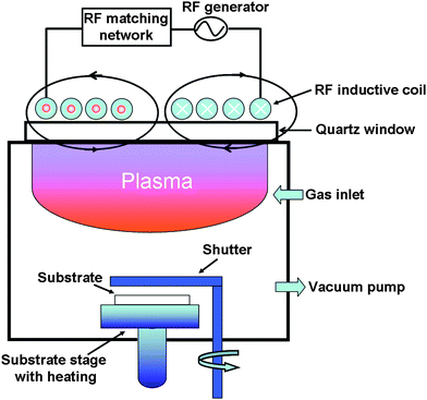 | ||
| Fig. 1 A schematic of the low-frequency inductively coupled plasma-assisted chemical vapor deposition system. | ||
In this work, a series of samples with different hydrogen dilution ratios was synthesized by changing the hydrogen gas flow rate while the silane gas flow rate, methane gas flow rate, inductive rf power, substrate temperature, and deposition time were kept fixed at 6.0 sccm (sccm denotes cubic centimetres per minute at standard temperature and pressure), 1.0 sccm, 1600 W, 200 °C, and 30 min, respectively. The plasma has a volume of ∼4.8 × 104 cm3, therefore the rf power density remained at a relatively low value of approximately 33.3 mW cm−3.21 The hydrogen gas flow rates were 70.0, 49.0, 28.0, 7.0, and 0.0 sccm, and thus the hydrogen dilution ratios X (defined as the flow rate ratio of hydrogen-to-silane plus methane gases) were 10.0, 7.0, 4.0, 1.0, and 0.0, respectively. These values of X are much smaller than those commonly used in similar capacitively coupled plasmas. The thickness of the synthesized films ranged from 198 to 600 nm.
The specimens were deposited on (100)-oriented single-crystalline silicon substrates for scanning electron microscopy (SEM), high-resolution transmission electron microscopy (HRTEM), X-ray diffraction (XRD), Raman scattering, X-ray photoelectron spectroscopy (XPS), and Fourier-transform infrared (FTIR) absorption spectroscopy measurements. The surface morphology and fracture cross-section of the deposited films were observed using a JEOL JSM-6700F field-emission scanning electron microscope fitted with a 30 kV electron gun. The HRTEM analysis was carried out through the use of a JEOL JEM-2010 electron microscope equipped with a 200 kV field-emission gun. The crystalline structure of the synthesized films was investigated using a Siemens D5005 X-ray diffractometer, operating in grazing-angle mode, wherein the incident X-ray wavelength was 1.54 Å (Cu Kα line) at 40 kV and 40 mA. The glancing angle between the incident X-ray and the film surface was fixed at 1°, and the diffraction pattern was obtained by changing the position of the counter. Raman measurements were undertaken using a Renishaw 1000 micro-Raman system using a 514.5 nm Ar+ laser for excitation. The chemical composition of the deposited films was studied ex situ using a VG ESCALAB 220i-XL X-ray photoelectron spectrometer using a Mg Kα (1253.6 eV) X-ray source. The IR absorption spectra were measured using Perkin-Elmer FTIR 1725X spectrometer in the mid-infrared range from 400 to 4000 cm−1.
3. Results
This section focuses on the investigation of the possibility of control of Si nanophase in the amorphous SiC matrix by varying the dilution ratios of the precursor gas mixtures with hydrogen. A broad range of advanced characterization tools including SEM, HRTEM, XRD, Raman, FTIR, XPS, etc. has been used for this purpose.The topography and microstructure of the nc–Si/a–SiC films were analyzed by SEM and HRTEM techniques. Fig. 2(a)–(c) shows the typical surface morphologies and cross-sections of the samples deposited at X = 0, 4.0, 10.0, respectively. As shown in Fig. 2(a), at X = 0, the morphology of the deposited sample features spherical-like clusters (with a typical size of a few to several tens of nanometres) with appreciable voids between the clusters. These clusters most likely have an amorphous structure as will be confirmed by the following XRD and Raman analyses. On the other hand, at X = 4.0 or 10.0, the films appear to be more compact and consist of small nanoparticles without any pronounced voids between them. In particular, at X = 10.0, it is evident that the film grows in a vertically aligned columnar structure and the interface between the Si substrate and the deposited film is smooth, clear, and free from major defects. This columnar structure is particularly useful for solar cell applications since it provides channels for effective carrier transport inside the film.14,20
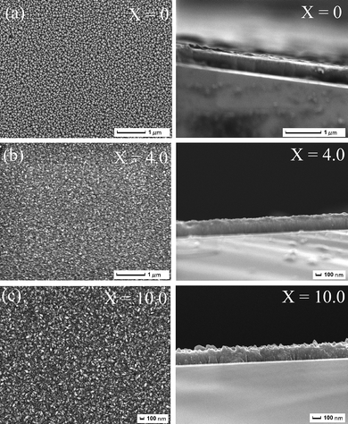 | ||
| Fig. 2 (a)–(c) Typical surface morphologies and cross-sections of the samples deposited at X = 0 (a), 4.0 (b), 10.0 (c), respectively. | ||
To reveal the microstructure of the deposited films at the atomic scale, the HRTEM measurements were undertaken. Fig. 3(a) shows a typical bright-field image of the sample deposited at X = 10.0. Since the atomic density of Si is higher than that of the SiC, the black dots appearing in the image should be attributed to Si QDs. One can notice that the Si QDs with a fairly uniform grain size are distributed throughout the scanned region. The inset of Fig. 3(a) presents a magnified HRTEM image of an individual Si QD. Clear lattice fringes can be observed and the lattice fringe spacing determined from this image approximately amounts to 3.1 Å, which corresponds to the (111) crystal plane of Si.11 This is why we conclude that Fig. 3(b) shows the size distribution histogram of the Si QDs observed in Fig. 3(a). This size distribution shows that the size of >60% of the nanocrystals falls within the narrow range 4–5 nm, which demonstrates the excellent uniformity of the Si quantum dots. Furthermore, the average size of the QDs determined from this histogram is 4.4 nm.
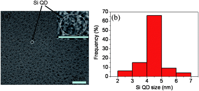 | ||
| Fig. 3 (a) A typical bright-field image of the sample deposited at X = 10.0. The inset of Fig. 3(a) shows a magnified HRTEM image of an individual Si quantum dot. (b) The size distribution histogram of the Si quantum dots observed in (a). | ||
The crystal structure of the nanophase nc–Si/a–SiC films under different hydrogen dilution ratios X was studied by XRD. Fig. 4 shows the XRD spectra of the samples deposited at X = 0–10.0. At X ≤ 1.0, no diffraction peaks attributed to the crystalline silicon are observed whilst at X = 4.0, small, broad but clearly resolved diffraction peaks at 2θ = 28.4°, 47.3°, and 56.1° appear. These peaks originate from the (111), (220), and (311) crystal planes of silicon, respectively.14,22 The occurrence of these three diffraction peaks suggests that the Si crystallites can be formed at X = 4.0. With the further increase of X, the intensities of all these diffraction peaks are gradually increased while the full widths at half maximum of all these diffraction peaks become smaller, indicating that the crystallite size becomes larger and the degree of crystallinity has further increased. Additionally, it is worthwhile to stress that no diffraction peaks attributed to crystalline SiC or crystalline forms of carbon (graphite or diamond) have been detected in the XRD spectra.
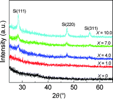 | ||
| Fig. 4 XRD spectra of the samples deposited at different hydrogen dilution ratios X from zero to 10.0. | ||
The crystallinity of the deposited films was further investigated by Raman spectroscopy. Fig. 5 presents the Raman scattering spectra of the samples deposited at different hydrogen dilution ratios X. At X ≤ 1.0, only one single broad peak centered at ∼480 cm−1 can be observed. This peak is attributed to the transverse optical (TO) mode of Si–Si vibrations in the amorphous phase, suggesting that the deposited film is completely amorphous.14,20 At X = 4.0, two pronounced peaks centered at ∼480 and 520 cm−1 can be observed; the latter peak is attributed to the TO mode of Si–Si vibrations in the crystalline phase.14,20 The appearance of the peak at 520 cm−1 in the spectrum suggests that the Si crystallites are formed in the film at X = 4.0. At X >4.0, the peak at 480 cm−1 disappears and the peak at 520 cm−1 becomes dominant, which indicates that the crystallinity degree of silicon nanocrystals is further improved with the further increase of X. However, one can also notice that the dominant peak at 520 cm−1 is not symmetric and features an extended tail towards small wavenumbers. This tail originates from the defective part of the crystalline phase due to the crystallite size effect and stress within the material.20,23 It is noteworthy that the Raman results are highly consistent with the XRD analysis.
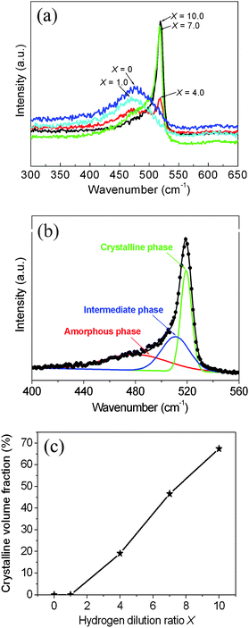 | ||
| Fig. 5 (a) Raman scattering spectra of the samples deposited at different hydrogen dilution ratios X. (b) A typical deconvolution of the Raman spectrum of the sample deposited at a hydrogen dilution ratio X = 10.0. (c) The estimated crystalline volume fraction of the nc–Si/a–SiC films as a function of the hydrogen dilution ratio X. | ||
In order to quantitatively characterize the crystallinity degree of the nc–Si/a–SiC films, the Raman scattering spectra (recorded in the wavenumber range between 400 and 560 cm−1) have been deconvoluted into three independent Gaussian peaks using a least-squares routine, after Shirley background subtraction.14,20 These three independent peaks are: (i) a crystalline silicon narrow peak in the vicinity of 520 cm−1; (ii) an intermediate peak between 500 and 510 cm−1 originating from small Si crystallites or grain boundaries; (iii) an amorphous silicon peak at approximately 480 cm−1.14,20Fig. 5(b) presents a typical deconvolution of the Raman spectrum of the sample deposited at a hydrogen dilution ratio X = 10.0. From the deconvoluted spectra, one can estimate the crystalline volume fraction of the deposited nc–Si/a–SiC films through the combined area of the individual crystalline and intermediate components divided by the total area of the individual crystalline, intermediate, and amorphous components.14,20
Fig. 5(c) shows the estimated crystalline volume fraction of the nc–Si/a–SiC films as a function of the hydrogen dilution ratio X. One can observe that at X ≤ 1.0, the crystalline volume fraction approximately equals to zero, while at X ≥ 4.0, the crystalline volume fraction increases in an almost linear fashion from 19.1% at X = 4.0 to 67.4% at X = 10.0.
The bonding configurations of the samples were studied by FTIR spectroscopy. Fig. 6 shows the FTIR spectra of the samples deposited at different hydrogen dilution ratios X. These spectra have been corrected for the substrate absorption, and normalized by the film thickness. The main absorption peaks appearing in the spectra are located at ∼640, ∼790, and ∼2100 cm−1, respectively. These peaks are attributed to the characteristic Si–H wagging or rocking mode, the stretching mode of Si–C bonds, and the Si–H/SiH2 stretching mode, respectively.21,24 With the decrease of X, the intensities of the peaks at 640 and 2100 cm−1 do not vary much whilst the intensity of the peak at 790 cm−1 increases significantly. This implies that an increasing number of carbon atoms are incorporated into the films to form Si–C bonds as X decreases. It is also worth mentioning that no absorption bands at around 2800–3000 cm−1 attributed to sp3 C–Hn (n = 1, 2, 3) or above 3000 cm−1 attributed to sp2 C–Hn (n = 1, 2, 3) have been observed.21,24 This indicates that almost all carbon atoms are bonded to silicon atoms.
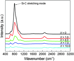 | ||
| Fig. 6 FTIR absorption spectra of the samples deposited at different hydrogen dilution ratios X. | ||
The elemental composition of the nanophase nc–Si/a–SiC films was measured by XPS. A beam of 2 keV argon ions was used to sputter the surface of the samples for 3 min to remove the surface contamination. Fig. 7(a) shows a typical wide-scan XPS spectrum of the sample deposited at a hydrogen dilution ratio X = 4.0. This spectrum clearly demonstrates the presence of Si, Ar, C elements and also a minor trace of oxygen.11 The emergence of the Ar peaks (Ar 2p and Ar 2s) in the spectrum stems from the Ar implantation into the surface of the films during the process of surface conditioning prior to the XPS measurement whilst the appearance of the small O peak (O 1s) is possibly due to residual oxygen in the growth chamber and/or residual surface contamination of the films.
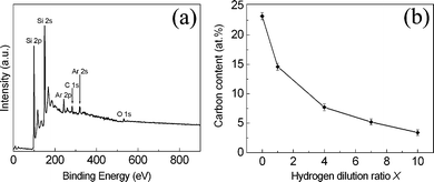 | ||
| Fig. 7 (a) A typical wide-scan XPS spectrum of the sample deposited at a hydrogen dilution ratio X of 4.0. (b) Carbon content of the deposited films as a function of the hydrogen dilution ratio X deduced by XPS. | ||
The carbon content of the nanophase nc–Si/a–SiC films, defined as the relative atomic concentration of the carbon element divided by the combined concentrations of the silicon and carbon elements, has been deduced from the XPS wide-scan spectra using the individual peak areas and elemental sensitivity factors (the sensitivity factors used in this work are 0.31 and 0.37 for carbon and silicon elements, respectively).11,25Fig. 7(b) displays the carbon content as a function of the hydrogen dilution ratio X. One can notice that, initially, the carbon content decreases very strongly from 23.2 at% at X = 0 to 7.7 at% at X = 4.0, and then is only slightly reduced with a further increase of X, reaching the lowest value of 3.4 at% at X = 10.0. This result is consistent with the FTIR analysis which indicates that more and more carbon atoms are incorporated into the films when X is decreased.
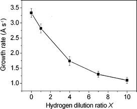
Finally, the film growth rate Rd was derived from the film thickness (measured by cross-sectional SEM) and the deposition time. Fig. 8 presents the growth rate Rd of the nc–Si/a–SiC films as a function of the hydrogen dilution ratio X. One can observe that Rd varies in the range 1.1–3.3 Å s−1 and becomes smaller with the increase of X. It is noteworthy that the maximum rate of change of the growth rate Rd occurs when the hydrogen dilution ratio X is increased from 1.0 to 4.0. This rapid variation of the growth rate Rd is closely related to the appearance of the Si nanocrystallites (QDs) in the film at X = 4.0.
 | ||
| Fig. 8 Growth rate Rd of the deposited films as a function of the hydrogen dilution ratio X. | ||
4. Discussion
Let us now interpret the experimental results presented in the previous section and propose the physical mechanisms responsible for the nanocrystalline Si phase (Si QDs) formation in an amorphous silicon carbide matrix. XRD, Raman, and SEM analyses show that with the increase of the hydrogen dilution ratio X, the crystallization of the silicon is improved and the phase transition from the amorphous to the crystalline state occurs at X = 4.0. Furthermore, the XPS and FTIR results indicate that an increasing number of carbon atoms are incorporated into the synthesized films when X is decreased. Therefore, we surmise that the addition of the hydrogen to the silane and methane precursor gases plays two important roles: (i) it favors the formation of Si QDs by reducing the free energy of certain crystalline facets; (ii) it reduces the carbon content of the deposited films by etching surface carbon atoms away.Let us now discuss the effect of hydrogen dilution on the growth (including nucleation, aggregation/coalescence, etc.) of the Si QDs embedded in the amorphous SiC matrix. According to the classic thermokinetic theory, the Gibbs free energy for an arbitrary nanoparticle can be expressed as
| G0x = Gbulkx + Gsurfacex + Gedgex + Gcornerx | (1) |
Precursors can be incorporated into the Si QDs by either directly landing on them from the gas/plasma phase or by depositing on the substrate first and travelling to the crystallites via surface diffusion.29,30 With the increase of X, the surface reactivity of the Si nuclei can be significantly reduced, which leads to a lower surface diffusion activation energy Ediff and a lower surface desorption energy Edes.14,31,32 The diffusion and desorption coefficients have the form
 | (2) |
 | (3) |
As discussed earlier, the increase in X decreases Ediff which in turn exponentially increases D as can be seen from eqn (2). This means that adradicals (adsorbed radicals) on the surface move much faster, and eventually find the optimum stacking points in the crystal lattice. In addition to this, the increase in X also decreases Edes which in turn increases the rates of desorption as reactive hydrogen atoms collide with Si adatoms on the surface and remove them. These effects strongly decrease the species residence time on the surface. This leads to lower rates of precursor incorporation into the developing QDs. Consequently the growth rates of the QDs decrease at higher hydrogen dilution ratios X as seen in Fig. 8. However, the higher mobility of adradicals due to a reduction in Ediff leads to more pronounced crystallization as suggested by the results in Figs. 4 and 5. Under such conditions, the adsorbed species move to the stacking points in the crystal lattice faster and are also removed much faster should they not incorporate into the developing lattice.33,34
As mentioned earlier, the XRD and Raman analyses have revealed the presence of Si nanocrystals when X ≥4.0. However, no crystalline SiC or crystalline forms of carbon have been found despite the presence of Si–C bonds in the films as detected by the FTIR. This implies that when X ≥4.0, some surface diffusion-assisted phase segregation takes place and leads to the encapsulation of Si QDs with amorphous SiC.29,35 SiC bonds can either form in the plasma (in this case SiC species deposit as ad-dimers) or from carbon adatoms which form bonds with Si atoms which already exist on the surface (either as part of the film/substrate or are adsorbed to the surface). The as-formed SiC ad-dimers move much slower on the film's surface and also require significantly more energy to desorb. On the other hand, C species have a relatively high mobility on the surface. However, the number of carbon species is significantly lower compared to the Si species. This is why it is less likely for large groups of C adatoms to assemble into carbon nanostructures. Under such conditions, carbon species prefer to form SiC bonds as new material arrives from the gas phase. Thus, carbon atoms are typically buried or bond with Si before forming crystals, eventually leading to the formation of the amorphous SiC matrix which develops simultaneously with the crystalline Si nanophase.29,35
In our series of experiments, the gas flow rates of silane and methane were kept fixed at 6 and 1 sccm, respectively. This implies that the concentrations of Si- and C-based radicals remain almost the same if the effect of the plasma-produced reactive hydrogen atoms is not taken into account. However, with the increased hydrogen dilution ratio X, the C-based weak or strained near-surface bonds (such as sp2 C or sp3 C) are more easily and effectively etched away from the growth surface by the hydrogen radicals compared to the Si-based strained bonds (such as sp3 Si).36,37 In addition to this, the C-based radicals have a lower sticking coefficient than the Si-based radicals.21 These considerations explain the experimental results that smaller numbers of carbon atoms are incorporated into the films at a higher value of X. It is noteworthy that the etching rate of the disordered material by the hydrogen radicals also increases with X, eventually leading to the lower growth rate at a higher hydrogen dilution ratio X observed in our experiments.
Variation of the hydrogen supply to the plasma reactor also significantly affects the production of reactive radicals in the discharge. For example, a silane molecule SiH4 can dissociate to form reactive silyl (SiH3) and H radicals, as well as many other species in a series of reversible reactions.29,38 The SiH3 radical is extremely reactive and plays an important role in the growth of the films. For instance, it can remove a H atom from a surface passivating layer and activate a Si dangling bond for the subsequent incorporation of another silyl radical into the growth surface. However, with the increased presence of H atoms which occurs at larger values of X, the lifetimes of such reactive species can decrease significantly. Indeed, a large number of H radicals will have an opportunity to react with many molecules and radicals as they deposit on the surface. As a result, the number of species which can actually stick to the substrate or crystallites is actually decreased.38 This is yet another effect which reduces the growth rate of the films.
We stress that, in comparison with the conventional (13.56 MHz) capacitively coupled rf plasmas, the ICP source used in our experiments features high-density plasmas and has an outstanding dissociation ability. As such, the large flux of hydrogen radicals on the growth surface required for the formation of Si nanocrystalline phase can be delivered by the effective dissociation of silane, methane, and hydrogen molecules in the ICP-based process even at a low hydrogen dilution ratio X of 4.0 rather than more than 100.0, commonly used in conventional capacitively coupled rf plasma-based processes. Physical mechanisms for the effective crystallization of nanocrystalline silicon or nanocrystalline cubic silicon carbide in high-density inductively coupled plasmas completely without hydrogen precursor gas or at low hydrogen dilution ratios X have been investigated previously.14,31,36,39
5. Conclusions
In this work, a simple, effective and innovative approach based on high-density, non-equilibrium inductively coupled plasmas has been proposed to synthesize crystalline Si quantum dots embedded in an amorphous SiC matrix from the gas mixture of the silane, methane and hydrogen. We have systematically studied the morphological, structural, and compositional properties of the deposited films under the conditions of different hydrogen dilution ratios X. It was found that with increasing hydrogen dilution ratio X, the crystallinity degree and the crystallite size increases while the growth rate and the carbon content are reduced. Our experimental results clearly demonstrate effective nanophase segregation with highly uniform Si QDs embedded in the amorphous SiC matrix formed at a low hydrogen dilution ratio X of 4.0. A viable physical mechanism based on the effect of hydrogen dilution on the nucleation and growth processes of the Si QDs in the high-density inductively coupled plasmas has been proposed to explain the obtained experimental results. Finally, these results are particularly important for the development of third-generation solar cells, light-emitting diodes, thin-film transistors, and some other emerging applicationsAcknowledgements
This work is partially supported by the National Research Foundation (Singapore), the Australian Research Council, and CSIRO (Australia). The authors thank S. Y. Huang for fruitful discussions and technical assistance.References
- G. F. Grom, D. J. Lockwood, J. P. McCaffrey, H. J. Labbé, P. M. Fauchet, B. W. Jr, J. Diener, D. Kovalev, F. Koch and L. Tsybeskov, Nature, 2000, 407, 358 CrossRef CAS.
- B. Zaknoon, G. Bahir, C. Saguy, R. Edrei, A. Hoffman, R. A. Rao, R. Muralidhar and K. M. Chang, Nano Lett., 2008, 8, 1689 CrossRef.
- V. I. Klimov, A. A. Mikhailovsky, S. Xu, A. Malko, J. A. Hollingsworth, C. A. Leatherdale, H. J. Eisler and M. G. Bawendi, Science, 2000, 290, 314 CrossRef CAS.
- R. E. Serda, S. Ferrati, B. Godin, E. Tasciotti, X. W. Liu and M. Ferrari, Nanoscale, 2009, 1, 250 RSC.
- C. Q. Sun, Prog. Mater. Sci., 2009, 54, 179 CrossRef CAS.
- T. S. Pui, A. Agarwal, F. Ye, Z. Q. Tou, Y. Huang and P. Chen, Nanoscale, 2009, 1, 159 RSC.
- P. F. Trwoga, A. J. Kenyon and C. W. Pitt, J. Appl. Phys., 1998, 83, 3789 CrossRef CAS.
- M. Xu, S. Xu, J. W. Chai, J. D. Long and Y. C. Ee, Appl. Phys. Lett., 2006, 89, 251904 CrossRef.
- A. Lacombe, F. Beaudoin, D. Koshel, D. Barba, F. Martin and G. G. Ross, Appl. Phys. Lett., 2009, 94, 012112 CrossRef.
- C. Q. Sun, Prog. Solid State Chem., 2007, 35, 1 CrossRef CAS.
- Q. J. Cheng, S. Xu and K. Ostrikov, Acta Mater., 2010, 58, 560 CrossRef CAS.
- U. Coscia, G. Ambrosone, S. Lettieri, P. Maddalena, V. Rigato, S. Restello, E. Bobeico and M. Tucci, Sol. Energy Mater. Sol. Cells, 2005, 87, 433 CrossRef CAS.
- T. Chen, Y. Huang, D. Yang, R. Carius and F. Finger, Phys. Status Solidi RRL, 2008, 2, 160 Search PubMed.
- Q. J. Cheng, S. Xu, S. Y. Huang and K. Ostrikov, Cryst. Growth Des., 2009, 9, 2863 CrossRef CAS.
- J. Li, J. Wang, M. Yin, P. Gao, D. He, Q. Chen, Y. Li and H. Shirai, J. Appl. Phys., 2008, 103, 043505 CrossRef.
- Q. J. Cheng, S. Xu, J. D. Long and K. Ostrikov, Appl. Phys. Lett., 2007, 90, 173112 CrossRef.
- Q. J. Cheng and S. Xu, J. Appl. Phys., 2007, 102, 056101 CrossRef.
- S. Xu, K. N. Ostrikov, Y. Li, E. L. Tsakadze and I. R. Jones, Phys. Plasmas, 2001, 8, 2549 CrossRef CAS.
- K. N. Ostrikov, M. Y. Yu and L. Stenflo, Phys. Rev. E: Stat. Phys., Plasmas, Fluids, Relat. Interdiscip. Top., 2000, 61, 782 CrossRef CAS.
- Q. J. Cheng, S. Xu and K. Ostrikov, Nanotechnology, 2009, 20, 215606 CrossRef.
- Q. J. Cheng, S. Xu, J. D. Long, Z. H. Ni, A. E. Rider and K. Ostrikov, J. Phys. D: Appl. Phys., 2008, 41, 055406 CrossRef.
- Y. Hotta, H. Toyoda and H. Sugai, Thin Solid Films, 2007, 515, 4983 CrossRef CAS.
- P. J. Alet, L. Yu, G. Patriarche, S. Palacin and P. R. i. Cabarrocas, J. Mater. Chem., 2008, 18, 5187 RSC.
- K. Chew, Rusli, S. F. Yoon, J. Ahn, V. Ligatchev, E. J. Teo, T. Osipowicz and F. Watt, J. Appl. Phys., 2002, 92, 2937 CrossRef CAS.
- Q. J. Cheng, J. D. Long and S. Xu, J. Appl. Phys., 2007, 101, 094304 CrossRef.
- A. S. Barnard, Nanoscale, 2009, 1, 89 RSC.
- I. Umezu, A. Sugimura, M. Inada, T. Makino, K. Matsumoto and M. Takata, Phys. Rev. B: Condens. Matter Mater. Phys., 2007, 76, 045328 CrossRef.
- M. Xu, S. Y. Huang, J. W. Chai, V. M. Ng, J. D. Long and P. Yang, Phys. E., 2006, 35, 81 CrossRef CAS.
- K. Ostrikov, Rev. Mod. Phys., 2005, 77, 489 CrossRef CAS.
- N. M. Hwang and D. Y. Kim, Int. Mater. Rev., 2004, 49, 171 Search PubMed.
- Q. J. Cheng, S. Xu and K. Ostrikov, J. Mater. Chem., 2009, 19, 5134 RSC.
- I. Levchenko, A. Rider and K. Ostrikov, Appl. Phys. Lett., 2007, 90, 193110 CrossRef.
- U. Cvelbar, Z. Q. Chen, M. K. Sunkara and M. Mozetič, Small, 2008, 4, 1610 CrossRef CAS.
- I. B. Denysenko, S. Xu, J. D. Long, P. P. Rutkevych, N. A. Azarenkov and K. Ostrikov, J. Appl. Phys., 2004, 95, 2713 CrossRef CAS.
- G. Abrasonis, G. J. Kovacs, A. Mücklich, S. Zhou, D. Babonneau and A. Martinavičius et al., J. Phys. Chem. C, 2009, 113, 8645 CrossRef CAS.
- Q. J. Cheng, S. Xu, J. D. Long and K. Ostrikov, Chem. Vap. Deposition, 2007, 13, 561 CrossRef CAS.
- S. Sriraman, S. Agrawal, E. S. Aydil and D. Maroudas, Nature, 2002, 418, 62 CrossRef CAS.
- J. Perrin, M. Shiratani, P. K. Nune, H. Videlot, J. Jolly and J. Guillon, J. Vac. Sci. Technol., A, 1998, 16, 278 CrossRef.
- Q. J. Cheng, S. Xu and K. Ostrikov, J. Phys. Chem. C, 2009, 113, 14759 CrossRef CAS.
| This journal is © The Royal Society of Chemistry 2010 |