Controllable construction of ZnO/TiO2 patterning nanostructures by superhydrophilic/superhydrophobic templates
Yuekun Laiab, Zequan Lina, Jianying Huangc, Lan Suna, Zhong Chenb and Changjian Lin*a
aState Key Laboratory for Physical Chemistry of Solid Surfaces, and College of Chemistry and Chemical Engineering, Xiamen University, Xiamen 361005, People’s Republic of China. E-mail: cjlin@xmu.edu.cn
bSchool of Materials Science and Engineering, Nanyang Technological University, 50 Nanyang Avenue, Singapore 639798, Singapore
cFujian Institute of Research on the Structure of Matter, Chinese Academy of Sciences, Fuzhou, 350002, People’s Republic of China
First published on 17th September 2009
Abstract
Position- and orientation-controllable micropatterned ZnO/TiO2 nanostructures with different morphologies have been fabricated using a novel and versatile superhydrophilic/superhydrophobic template. Scanning electron microscopy, optical microscopy, electron probe microanalysis and X-ray diffraction were systematically used to confirm the successful fabrication of the patterns and to characterize the structure and morphology. The selective growth of ordered ZnO nanostructured patterns on the TiO2 nanotube surface employs a simple photocatalytic lithography technique with mild reaction conditions and in the absence of seeds and noble metal catalysts. The photoelectrical properties of the micropatterned ZnO/TiO2 nanocomposites with unique heterojunction structure and different density and orientation of the ZnO crystals were also investigated. It is expected that this novel micropatterned technique based on the superhydrophilic/superhydrophobic template will become a powerful tool for fabricating various types of micropatterned nanomaterials and devices.
1. Introduction
Wettability of solid surfaces is one of the important properties that is governed by both the chemical composition and geometrical structure.1–4 Extreme wettability contrast (i.e. superhydrophilic/superhydrophobic) is a potentially powerful and economical approach to precisely construct nanostructures in aqueous solution. So far, only few reports on the fabrication and application of superhydrophilic/superhydrophobic patterning are available.5–9The deposition of ZnO nanostructures on a variety of substrates has attracted great attention due to its wide applications in sensing,10–12 optoelectronics13–15 and light emitting displays.16–18 Moreover, the controlled growth and synthesis of ZnO nanostructures on large scale is of particular importance in making new types of functional semiconductor devices and constructing micro- and nano-electromechanical systems (MEMS/NEMS).19–21 To control the resulting ZnO properties, an appropriate choice of synthesis and processing parameters plays a crucial role. Over the past few years, nanostructured ZnO periodic patterns have been created using seed layers,22,23 noble metal catalysts,24–26 patterned photoresists27 and mold replication on smooth substrates.28,29 For example, Sun et al.23 reported ZnO patterns using a hydrothermal approach assisted by spin-coating a ZnO seed layer. Yu and co-authors26 successfully fabricated ordered ZnO nanorod patterns on Si substrates through an Au catalytic vapor–liquid–solid process. Although they could provide precise position control, the involvement of complicated equipment and the strict requirements of the processing steps and environment have limited the practical usefulness in fabricating large areas of nanostructures in a high-throughput fashion. Therefore, the extension of a mild, low-cost bottom-up synthetic route that does not require vacuum technologies and seed/catalyst layers is highly desired. Recently, Song et al.30,31 developed a novel biomimetic approach for selective assembly of nanostructured semiconductor patterned films onto flexible polymer substrates treated with a simple UV exposure carboxylation process.
In this paper, we propose a novel seed/catalyst-free patterning process based on an extreme wettability contrast (superhydrophilic/superhydrophobic) template to fabricate position- and orientation-controlled large-scale ZnO nanorod patterns on TiO2 nanotube array surfaces. Specifically, our strategy involves the formation of enhanced wettability contrast template first, followed by selective growth of ZnO nanostructures in the superhydrophilic regions. In the superhydrophobic regions, the growth is suppressed. This special template can be utilized to generate different nanostructured ZnO patterns with clearly defined edges. Our approach, in contrast to others, offers several advantages including extraordinary versatility (fabrication performed under ambient conditions), low cost, and non-reliance on potentially harmful metal catalyst (or seeding layer). Hence, this novel method is particularly useful and promising in fabricating functional nanostructures on a large scale.
2. Experimental
2.1 Preparation of superhydrophilic/superhydrophobic pattern
Titanium (≥99.5%) sheets were anodized with a Pt counter electrode in 0.5 wt% HF electrolyte solution under 20 V for 20 min to fabricate TiO2 nanotube arrays, as reported in more detail previously.32–35 The as-prepared amorphous TiO2 nanotube films were calcined at 450 °C for 2 h to form the crystalline anatase phase. The nanotube structures were then treated in a methanolic solution of hydrolyzed 1 wt% 1H,1H,2H,2H-perfluorooctyltriethoxysilane (PTES, Degussa Co., Ltd.) for 1 h, and subsequently heated at 140 °C for 1 h to remove residual solvent. Superhydrophobic patterns were obtained by selective exposure to a 200 W high-pressure mercury lamp (maximum intensity at 365 nm, 100 mW cm−2) under ambient conditions for 20 min through a photomask placed on its surface. The light irradiation photocatalytically cleaves the hydrophobic fluoroalkyl chain of PTES,7,36 turning the rough surface from superhydrophobic to superhydrophilic.2.2 ZnO nanorod patterning
The vertical ZnO nanorod arrays were prepared by an electric field assisted deposition method.30 Precursor solutions were prepared by dissolving zinc nitrate hexahydrate (Zn(NO3)2·6H2O, ≥99%) and hexamethylenetetramine (C6H12N4, ≥99%) in doubly deionized water. The concentration of zinc and amine were fixed at 5 mM. A piece of Pt plate acted as the counter electrode. During ZnO deposition the resistive voltage may drop across the cell preventing potential-dependent deposition and thus a constant current density of 0.25 mA cm−2 at 90 °C was used for 3 min. The deposited sample was then picked up from the container and thoroughly rinsed with distilled water and dried in air. For a comparative study, ZnO nanostructured crystal patterned samples were also investigated by direct liquid phase deposition without the presence of electric field under identical experimental conditions (the patterning surface placed upward).2.3 Material characterizations
The morphology and composition of the patterns were observed by a field-emission scanning electron microscope (FESEM, LEO-1530, Germany) combined with energy dispersive spectroscopy (EDS). The chemical element distribution was measured by an electron probe microanalyzer (EPMA, JEOL JXA-8100, Japan). The crystallinity of the samples before and after annealing treatment was measured using an X-ray diffractometer with Cu-Kα radiation (XRD, Phillips X’pert-PRO PW3040). The water contact angle was measured with an optical contact angle meter system (Dataphysics, OCA-20) at ambient temperature. The water droplets used for the static contact angle and sliding angle measurements were 4 and 7 mg, respectively. The values reported are the average of five drops per sample at different locations. For fluorescence experiments, the obtained patterns were stained with fluorescein sodium, and observed by a Karl Zeiss fluorescence microscope (Axioskop2, MAT). The patterned TiO2 nanotube array samples were observed by optical microscopy (Eclipse E600, Nikon). Atom force microscopy (AFM) in tapping mode was performed on a Nanoscope IIIa (Digital Instrument Co., USA). For confocal microscopy, a Leica TCS SP5 with a He/Ne laser and fluotar objective, was used to investigate the morphology of the materials at micrometer scale. These measurements produced three-dimensional maps of the surfaces.2.4 Photocurrent measurements
The photocurrent action spectra were measured in a home-built two-electrode configuration experimental system, where the as-synthesized ZnO/TiO2 nanocomposite film served as the working electrode with an active area of about 1 cm2. A platinum wire was used as the counter electrode in the supporting electrolyte of 0.1 M aqueous Na2SO4 solution. A 150-W Xe lamp with a monochromator was used as the light source. The generated photocurrent signal was collected by using a lock-in amplifier synchronized with a light chopper. All measurements were controlled automatically by a microcomputer.3. Results and discussion
The fabrication process involves three main steps, as schematically illustrated in Fig. 1. First, a superhydrophobic titania nanotube array surface was fabricated using an electrochemical anodizing method and a self-assembling monolayer (SAM) technique (step 1 in Fig. 1). Second, the superhydrophilic/superhydrophobic micropattern was transferred to the substrate by a previously established photocatalytic lithography technique using a photomask. Finally, ZnO nanostructured crystals were grown on the titania micropattern in the absence or presence of an electric fields. Details of each step are described in the Experimental section.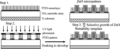 | ||
| Fig. 1 Schematic illustration of the fabrication procedure of ZnO nanocrystal micropatterns based on a superhydrophilic/superhydrophobic template. First, superhydrophobic TiO2 nanotube array films were formed on the titanium substrate (step 1). Then the superhydrophilic/superhydrophobic micropatterns were prepared by photocatalytic lithography with a photomask (step 2). Finally, the ZnO nanostructures were grown on the patterned template in the absence or presence of an electric field (step 3). | ||
Fig. 2(a) shows a typical FESEM image of the substrate before electrochemical anodization. The surface of the titanium substrate was relatively smooth, with features of polished ridges, grooves and pits at the micron scale. After anodization, some unevenness was observed, shallow cavities as large as several micrometers in diameter were present on the surface of the sample (Fig. 2(b)). This is probably due to the anisotropic oxidation of the underlying Ti grains.37–39 From the high magnification image (Fig. 2(c)), it can be seen that vertically oriented TiO2 nanotubes with inner diameter of approximately 80 nm covered the entire surface including the shallow polygonal micropits. The side view image shows that the self-assembled layers of the TiO2 nanotubes were open at the top and closed at the bottom with thickness about 350 nm (inset of Fig. 2(c)). The inset of Fig. 2(b) shows the intrinsic contact angle (CA) on the as-prepared vertically aligned TiO2 nanotube surface and its corresponding PTES modified surface is nearly 0° (superhydrophilic) and 156° (superhydrophobic), respectively. Moreover, the sliding angle of a 7 mg water droplet on the PTES modified TiO2 nanotube sample is 12.1 ± 1.9°, indicating a medium adhesive strength of water droplets on such vertical nanostructures due to its typical “line-contact” behavior.4 However, the CA for the “flat” TiO2 surface and its corresponding PTES modified sample is about 46° (hydrophilic) and 115° (hydrophobic), respectively. From these results, we know the top surface of the vertically aligned nanotubes has an amplification effect to make hydrophilic and hydrophobic surfaces become superhydrophilic and superhydrophobic, respectively. After UV irradiation for 30 min, the water CA on the TiO2 nanotube film and “flat” TiO2 film decreased to 0° and 26°, as a consequence of the photocatalytic activity of TiO2 films.40,41 Water droplets can quickly spread and wet the as-grown vertically aligned TiO2 nanotube film due to the side penetration of liquid by capillary forces in the special tubular structure. Moreover, after the UV irradiation, the sample showed hydrophobic character once again when it was treated with PTES. Therefore the surface can be reversibly switched between superhydrophobic and superhydrophilic by alternating SAM and UV photocatalysis on the rough TiO2 nanotube arrays (shown in Fig. 2(d)). Compared with the large wettability contrast on this type of rough surface (larger than 150°), the wettability of a “flat” TiO2 film can only be reversibly changed within the small range between 26 and 115°.
 | ||
| Fig. 2 SEM images of the mechanically polished and cleaned titanium substrate (a), low magnification of a nanotube structured TiO2 film (b), and a higher magnification of the TiO2 nanotube array film (c). Reversible surface wettability on a “flat” TiO2 film and rough nanotube TiO2 film by alternating SAM and UV photocatalysis (d). The inset of (b) shows the shape of a water drop on the PTES-modified and UV-irradiated TiO2 nanotube array film. The inset of (c) shows the side view of a TiO2 nanotube array film. | ||
The fabrication of superhydrophilic/superhydrophobic micropatterns (Fig. 3(a)) on TiO2 nanotube array films is described in the Experimental section. To verify the resulting micropatterns, fluorescein sodium was used as a probe to label the patterning surface. Fig. 3(b) shows the fluorescent micrograph of the resultant superhydrophilic/superhydrophobic micropatterns on TiO2 nanotube films. As shown, geometrically identical bright green superhydrophilic regions (microdots with a diameter of 50 μm) and dark superhydrophobic regions transferred well from the photomask to form a well-defined pattern. The UV irradiated regions become superhydrophilic owing to the photocatalytic cleavage of PTES molecules and the enhanced roughness of the nanotube structures, while the non-irradiated parts remain superhydrophobic without any change. Since the difference of the water CA between the irradiated and non-irradiated regions is larger than 150°, liquid containing fluorescent probe selectively and uniformly resides only on the superhydrophilic areas, not the neighboring superhydrophobic regions. Therefore, a clearly defined fluorescent pattern in line with the dimensions of the photomask could be obtained through wettability contrast. In addition, such a surface micropattern could potentially be used in erasable and rewritable mode due to the efficient photocatalytic activity of this special TiO2 nanostructure.
 | ||
| Fig. 3 Optical micrographs of the as-prepared superhydrophilic/superhydrophobic microtemplate (a), fluorescence microscopic image of the fluorescein probe on the corresponding superhydrophilic/superhydrophobic microtemplate (b), and the resulting patterned microarrays of ZnO/TiO2 nanostructures (c). | ||
On the basis of this patterning template, we exploited the extremely large wettability contrast between superhydrophilic regions and the adjacent superhydrophobic areas to precisely induce ZnO nanostructure deposition by several techniques. Fig. 3(c) shows the optical micrograph of the as-prepared ZnO/TiO2 micropattern (by electric field assisted deposition for 3 min) based on superhydrophobic/superhydrophilic micropatterns on the TiO2 nanotube array surface. It can be seen that the patterning shape of the ZnO crystals is the same as the template used.
Fig. 4 shows representative top-view FESEM images of the ZnO/TiO2 micropatterns by liquid-phase deposition after different times. After growth for 30 min (Fig. 4(a) and (b)), the nucleation and growth of ZnO crystals with various morphologies and sizes (nanoparticles and nanorods) are sparsely dispersed within the predefined superhydrophilic regions. In the superhydrophobic regions, the nanotube structure is retained with its original morphology due to the indirect contact with the solution and the effective protection by the PTES monolayer. Upon further increase in the deposition time to 90 min (Fig. 4(c) and (d)), it was observed that ZnO nanorods were the predominant structural features. The average diameter of the grown ZnO nanorods increases greatly to about 400–800 nm in diameter and 3–5 μm in length, which may be due to lower nucleation rate and higher growing space for ZnO nanorods. The superhydrophilic microdots are almost covered with randomly lying ZnO nanorods. Moreover, there are different growth orientations and some connections into adjacent nanorods. It is of interest to note that a two-dimensional (2D) pattern with smaller density of randomly packed ZnO nanorods, instead of the 3D pattern consisted of well-aligned vertical nanorods, which were confined and grown within the superhydrophilic regions.
 | ||
| Fig. 4 SEM images of the patterned ZnO nanostructured micropatterns by liquid phase deposition at 90 °C for different times: (a, b) 30 min; (c, d) 90 min. | ||
For practical application of thin film devices, the position- and orientation-control of ZnO nanorods are very important because they directly relate to their physical and chemical performances.42,43 In order to precisely control the spatial orientation of the ZnO nanostructures, we developed a new technique which is able to make the ZnO nanorods grow along the vertically aligned titania nanotubes rather by disordered deposition on the titania nanotube array surface. In this technique, resistance discrepancy was adopted to make the entrance of the tubes more conductive than the bottom of the tubes, to induce the epitaxial growth with spatial organization of uniform ZnO nanorods along the direction of the nanotubes. The quasi-perpendicular ZnO nanorods nucleate and grow uniformly and selectively throughout the superhydrophilic regions of the TiO2 nanotube surface by electric field assisted deposition at 90 °C for 3 min, while no nanorods are observed in the superhydrophobic regions (Fig. 5(a) and (b)). The EDS spectra also reveal that the presence of Zn, Ti and O elements on the superhydrophilic regions, while the elemental components in the superhydrophobic areas are only Ti and O. The inset of Fig. 5(b) shows the hexagonal end facet of a vertically aligned ZnO nanorod with a diameter about 100–150 nm growing on top of the TiO2 nanotube array surface. Therefore, the density, size and orientation of ZnO nanorods are very sensitive to the presence of electric fields.
 | ||
| Fig. 5 Typical SEM images of (a, b) the vertically aligned ZnO nanorods selectively grown on superhydrophilic patterning regions by the developed electric field assisted deposition technique at 90 °C for 3 min. 3D AFM image of the ZnO/TiO2 micropattern (c). Confocal microscopy image of the perpendicular ZnO nanorod array (d). The inset in (a) shows the side view SEM image of the corresponding ZnO nanorod pattern. (b) Shows the higher magnified SEM image of a ZnO nanorod with hexagonal end facet. | ||
A 3D AFM profile image (Fig. 5(c)) shows that the microscopic structure of the ZnO crystal deposition consisted in dense column arrays, which are induced and directed by the wettability template. The thickness of vertical ZnO nanorod film is in the range of 800–900 nm. Furthermore, the three-dimensional confocal microscopy image (Fig. 5(d)) also shows that the growth of the ZnO nanorod pattern is identical with the superhydrophilic/superhydrophobic template. Moreover, the Zn and O element distribution mappings measured by EPMA provide convincing evidence that the ZnO nanorods were only present in the superhydrophilic regions (Fig. 6(a) and (b)). The reason for the success of large area fabrication of well-defined patterns with clear boundaries is that the superhydrophobic regions covered by the PTES monolayers were isolated from the aqueous solution during the deposition. Fig. 6(c) and (d), shows the line-scan signal intensity profiles of zinc and oxygen elements across the pattern obtained after electric field assisted deposition for 3 min. It can be seen that both the line profiling of zinc and oxygen signal intensity increased greatly within the superhydrophilic regions. This suggests that most or all of the TiO2 surface areas corresponding to the superhydrophilic regions were homogeneously covered by ZnO nanorods, while the superhydrophobic regions remained almost unchanged due to the suppression by the air trapped in the nanotubes and the crevices between nanotubes.4 This image agrees well with the observed results by FESEM. The slight deviation of the detected signal intensity was due to analytical errors caused by the rough nanostructures.
 | ||
| Fig. 6 The chemical composition of area-scan and line-scan signal intensity mapping of Zn (a, c) and O (b, d) of the vertical ZnO nanorod micropattern on a TiO2 nanotube array surface after electric field assisted deposition for 3 min. | ||
Fig. 7 shows the XRD patterns of the ZnO/TiO2 coupled nanocomposites, which provide further insight into the crystal structure and orientation of the assembled ZnO nanocrystals. The as-prepared TiO2 nanotube array film on metal Ti substrate before annealing did not show any TiO2 peaks indicating the crystal structure of the TiO2 was amorphous (Fig. 7(a)). For the TiO2 nanotube films calcined at 450 °C for 2 h the new peaks can be well indexed as phase-pure anatase TiO2 (Fig. 7(b)). The ZnO/TiO2 film obtained by direct liquid phase deposition (Fig. 7(c)) shows only a weak diffraction peak for ZnO since the ZnO deposition rate was very low and the quantity was not sufficient to give a strong signal. In the case of the prepared ZnO nanorods by electric field assisted deposition (Fig. 7(d)), three obviously characteristic peaks (2θ = 31.77, 34.42 and 36.25°), marked by their Miller indices ((100), (002) and (101)) were observed. This reveals that the resultant ZnO nanorods were in the wurtzite phase (JCPDS no. 36-1451). Compared to the TiO2 mono-component nanomaterials, the coupled nanocomposites indeed consisted of both anatase TiO2 and wurtzite ZnO after annealing, which is clearly shown in the XRD pattern. Furthermore, the (002) diffraction peak of well-oriented vertical ZnO nanorods induced and directed by the perpendicular nanotube array structure using the electric field assisted technique exhibit greater intensity than that of the randomly packed ZnO nanorods by regular liquid phase deposition, indicating the highly preferential growth of the ZnO nanorods along the c axis and perpendicularly to the substrate surface (see the inset in Fig. 7). These XRD results agreed with the SEM observation and demonstrate that the orientation-controlled growth of ZnO nanostructures can be effectively realized by use of a predefined extreme wettability contrast template on a TiO2 nanotube array surface.
 | ||
| Fig. 7 XRD patterns of the as-prepared TiO2 nanotube film (a), TiO2 nanotubes (b) and ZnO/TiO2 nanocomposites prepared by direct liquid phase deposition (c) and electric field assisted deposition (d) upon sintering in air at 450 °C for 2 h. A, Z and T represent anatase TiO2, ZnO and Ti substrate, respectively. The inset image shows an enlarged view of the ZnO peaks. | ||
In order to examine the structure-specific properties of the nanostructured ZnO/TiO2 hybrid materials, measurements of the photocurrent action spectra were performed in a home-built photoelectrochemical measurement system. The results of photocurrent actions for all the samples, which were collected in the range from 250 to 500 nm are shown in Fig. 8. As shown, the as-prepared amorphous TiO2 nanotube sample showed no photocurrent response, while the annealed TiO2 and ZnO/TiO2 nanocomposites exhibited obvious photocurrent responses with maximum wavelength at 320 and 340 nm, respectively, which were blue-shifted from the band gap of bulk TiO2 (387 nm, 3.2 eV) and ZnO (368 nm, 3.37 eV) due to the quantum confinement effect.44 In the case of the prepared coupled ZnO/TiO2 nanocomposites, the photocurrent was found to be largely enhanced with higher photocurrent intensities than that of the compact TiO2 film obtained directly by thermal oxidation at 450 °C for 2 h. Furthermore, because of the synergistic effect, the photocurrent spectrum of the coupled ZnO/TiO2 nanocomposite was slightly blue-shifted from that of the ZnO nanorods. Interestingly, the photoelectrodes of the ZnO/TiO2 nanocomposites showed a smaller photocurrent spectrum (300–400 nm) than that of the monocomponent TiO2 nanomaterials (275–400 nm). Moreover, all the ZnO/TiO2 coupled heterojunctions exhibited moderate photocurrent intensity between that of the compact TiO2 film and the TiO2 nanotube film. It is also found that the photocurrent intensities of the resultant coupled ZnO/TiO2 nanocomposite decreased with an increase of the deposition time whether an electric field was present or absent. The beneficial influence of a lower degree of ZnO deposition agrees with the report by Kim45 and Yoon et al.46 Also, the generated photocurrent of the well-oriented perpendicular ZnO nanorod electrode prepared by electric field assisted deposition was much higher than that of the randomly distributed ZnO nanorod electrode. This may be attributed to that the vertical and more even ZnO nanorod film on the TiO2 nanotubes allows for more efficient electron transfer and greater surface area at the intimate ZnO/TiO2 heterojunctions. Light harvesting and charge transfer within such 3D organized junctions with well aligned vertical ZnO morphology are enhanced. These results demonstrate the importance of optimizing coupled nanostructured electrodes in an orderly orientation. Indeed, the photocurrent response of the micropatterned ZnO/TiO2 composite depends on many structural factors, which should be further studied.
 | ||
| Fig. 8 Photocurrent spectra of (a) amorphous TiO2 nanotube electrode, (b) compact TiO2 film electrode, (c) anatase TiO2 nanotube electrode, (d) vertically aligned ZnO nanorod micropattern on TiO2 nanotube surface (1.5 min), (e) vertically aligned ZnO nanorod micropattern on TiO2 nanotube surface (3 min), (f) randomly lying ZnO nanorod micropattern on TiO2 nanotube surface (30 min) and (g) randomly lying ZnO nanorod micropattern on TiO2 nanotube surface (90 min). | ||
The advantages of this simple approach lie in its generality and high selectivity for solution-based deposition without the presence of noble metal catalyst, and it can be easily extended to other coupled nanostructured materials of any arbitrary shape. In addition, with such versatile assembly of functional nanomaterials based on superhydrophilic/superhydrophobic templates, it is possible to open a new avenue to micro- and nanodevice fabrication and enable applications in a wide variety of fields such as microfluidic devices,47 biotechnology,48,49 water harvesting surfaces,50 and site-selective deposition templates,51,52etc.
4. Conclusion
In summary, we have demonstrated a successful application using a superhydrophilic/superhydrophobic template for position- and orientation-controlled growth of ZnO nanorods on TiO2 nanotube array surfaces. Spatial organization of ZnO crystals over large areas can be achieved with excellent selectivity. The micropatterned ZnO/TiO2 nanocomposite showed a better photocurrent response due to its unique heterojunction structure. These novel nanostructure patterning strategies based on wettability contrast can also be expanded to direct the deposition of other nanostructured materials from aqueous solution, which opens up avenues for potential applications in nanomaterials and technologies.Acknowledgements
The authors thank the financial supports from the National Natural Science Foundation of China (20773100, 50571085 and 20620130427), National Basic Research Program of China (2007CB935603), and the International Scientific and Technological Cooperation Projects of MOST (2007DFC40440).References
- R. Wang, K. Hashimoto, A. Fujishima, M. Chikuni, E. Kojima, A. Kitamura, M. Shimohigoshi and T. Watanabe, Nature, 1997, 388, 431 CrossRef CAS.
- K. Ichimura, S. K. Oh and M. Nakagawa, Science, 2000, 288, 1624 CrossRef CAS.
- X. F. Gao and L. Jiang, Nature, 2004, 432, 36 CrossRef CAS.
- Y. K. Lai, X. F. Gao, H. F. Zhuang, J. Y. Huang, C. J. Lin and L. Jiang, Adv. Mater., 2009 DOI:10.1002/adma.200900686.
- K. Tadanaga, J. Morinaga, A. Matsuda and T. Minami, Chem. Mater., 2000, 12, 590 CrossRef CAS.
- A. Matsuda, T. Sasaki, K. Tadanaga, M. Tatsumisago and T. Minami, Chem. Mater., 2002, 14, 2693 CrossRef CAS.
- Y. K. Lai, C. J. Lin, H. Wang, J. Y. Huang, H. F. Zhuang and L. Sun, Electrochem. Commun., 2008, 10, 387 CrossRef CAS.
- X. T. Zhang, O. Sato and A. Fujishima, Langmuir, 2004, 20, 6065 CrossRef CAS.
- X. T. Zhang, M. Jin, Z. Y. Liu, D. A. Tryk, S. Nishimoto, T. Murakami and A. Fujishima, J. Phys. Chem. C, 2007, 111, 14521 CrossRef CAS.
- A. A. Tomchenko, G. P. Harmer, B. T. Marquis and J. W. Allen, Sens. Actuators B, 2003, 93, 126 CrossRef.
- Z. Y. Fan, D. W. Wang, P. C. Chang, W. Y. Tseng and J. G. Lu, Appl. Phys. Lett., 2004, 85, 5923 CrossRef CAS.
- P. Mitra, A. P. Chatterjee and H. S. Maiti, Mater. Lett., 1998, 35, 33 CrossRef CAS.
- M. H. Huang, S. Mao, H. Feick, H. Q. Yan, Y. Y. Wu, H. Kind, E. Weber, R. Russo and P. D. Yang, Science, 2001, 292, 1897 CrossRef CAS.
- X. D. Wang, C. J. Summers and Z. L. Wang, Nano Lett., 2004, 4, 423 CrossRef CAS.
- Z. L. Wang, J. Phys.: Condens. Matter, 2004, 16, R829 CrossRef CAS.
- N. Saito, H. Haneda, T. Sekiguchi, N. Ohashi, I. Sakaguchi and K. Koumoto, Adv. Mater., 2002, 14, 418 CrossRef CAS.
- Y. Masuda, M. Yamagishi, W. S. Seo and K. Koumoto, Cryst. Growth Des., 2008, 8, 1503 CrossRef CAS.
- J. M. Bao, M. A. Zimmler, F. Capasso, X. W. Wang and Z. F. Ren, Nano Lett., 2006, 6, 1719 CrossRef CAS.
- J. H. He, J. H. Hsu, C. W. Wang, H. N. Lin, L. J. Chen and Z. L. Wang, J. Phys. Chem. B, 2006, 110, 50 CrossRef CAS.
- J. H. Hwang, L. W. Chen, T. C. Chen, C. W. Kuo, Z. S. Hu, T. R. Tsai, Y. J. Wu, T. Y. Lin, Y. Y. Jhuo, C. Y. Cheng, C. M. Lin and Y. H. Liu, Nanotechnology, 2009, 20, 055302 CrossRef.
- J. W. P. Hsu, Z. R. Tian, N. C. Simmons, C. M. Matzke, J. A. Voigh and J. Liu, Nano Lett., 2005, 5, 83 CrossRef CAS.
- Y. Masuda, S. Ieda and K. Koumoto, Langmuir, 2003, 19, 4415 CrossRef.
- H. K. Sun, M. Luo, W. J. Weng, K. Cheng, P. Y. Du, G. Shen and G. R. Han, Nanotechnology, 2008, 19, 395602 CrossRef.
- H. J. Fan, W. Lee, R. Scholz, A. Dadgar, A. Krost, K. Nielsch and M. Zacharias, Nanotechnology, 2005, 16, 913 CrossRef CAS.
- N. Saito, H. Haneda, T. Sekiguchi, T. Ishigaki and K. Koumoto, J. Electrochem. Soc., 2004, 151, H169 CrossRef CAS.
- C. W. Yu, S. H. Lai, T. Y. Wang, M. D. Lan and M. S. Ho, J. Nanosci. Nanotechnol., 2008, 8, 4377 CrossRef CAS.
- E. C. Greyson, Y. Babayan and T. W. Odom, Adv. Mater., 2004, 16, 1348 CrossRef.
- M. J. Hampton, S. S. Williams, Z. Zhou, J. Nunes, D. H. Ko, J. L. Templeton, E. T. Samulski and J. M. DeSimone, Adv. Mater., 2008, 20, 2667 CrossRef CAS.
- Y. F. Wang, X. L. Chen, J. H. Zhang, Z. Q. Sun, Y. F. Li, K. Zhang and B. Yang, Colloids Surf., A, 2008, 329, 184 CrossRef CAS.
- S. A. Morin, F. F. Amos and S. Jin, J. Am. Chem. Soc., 2007, 129, 13776 CrossRef CAS.
- F. F. Amos, S. A. Morin, J. A. Streifer, R. J. Hamers and S. Jin, J. Am. Chem. Soc., 2007, 129, 14296 CrossRef CAS.
- D. W. Gong, C. A. Grimes and O. K. Varghese, J. Mater. Res., 2001, 16, 3331 CrossRef CAS.
- L. V. Taveira, J. M. Macak, H. L. Tsuchiya, F. P. Dick and P. Schmuki, J. Electrochem. Soc., 2005, 152, B405 CrossRef CAS.
- J. L. Tao, J. L. Zhao, C. C. Tang, Y. R. Kang and Y. X. Li, New J. Chem., 2008, 32, 2164 RSC.
- Y. K. Lai, C. J. Lin, J. Y. Huang, H. F. Zhuang, L. Sun and T. Nguyen, Langmuir, 2008, 24, 3867 CrossRef CAS.
- Y. K. Lai, L. Sun, Y. C. Chen, H. F. Zhuang, C. J. Lin and J. W. Chin, J. Electrochem. Soc., 2006, 153, D123 CrossRef CAS.
- G. A. Crawford and N. Chawla, Acta Mater., 2009, 57, 854 CrossRef CAS.
- G. A. Crawford and N. Chawla, Scr. Mater., 2009, 60, 874 CrossRef CAS.
- K. Yasuda, J. M. Macak, S. Berger, A. Ghicov and P. Schmuki, J. Electrochem. Soc., 2007, 154, C472 CrossRef CAS.
- E. Balaur, J. M. Macak, L. Taveira and P. Schmuki, Electrochem. Commun., 2005, 7, 1066 CrossRef CAS.
- Y. K. Lai, H. F. Zhuang, L. Sun, Z. Chen and C. J. Lin, Electrochim. Acta, 2009, 54, 6536 CrossRef CAS.
- K. Koumoto, N. Saito, Y. F. Gao, Y. Masuda and P. X. Zhu, Bull. Chem. Soc. Jpn., 2008, 81, 1337 CrossRef CAS.
- Y. Masuda, N. Kinoshita, F. Sato and K. Koumoto, Cryst. Growth Des., 2006, 6, 75 CrossRef CAS.
- G. Wang, Q. Wang, W. Lu and J. H. Li, J. Phys. Chem. B, 2006, 110, 22029 CrossRef CAS.
- K. E. Kim, S. R. Jang, J. Park, R. Vittal and K. J. Kim, Sol. Energy Mater. Sol. Cells, 2007, 91, 366 CrossRef CAS.
- K. H. Yoon, J. Cho and D. H. Kang, Mater. Res. Bull., 1999, 34, 1451 CrossRef.
- B. Zhao, J. S. Moore and D. J. Beebe, Science, 2001, 291, 1023 CrossRef CAS.
- H. Sorribas, C. Padeste and L. Tiefenauer, Biomaterials, 2002, 23, 893 CrossRef CAS.
- Y. Ito, Biomaterials, 1999, 20, 2333 CrossRef CAS.
- L. Zhai, M. C. Berg, F. C. Cebeci, Y. Kim, J. M. Milwid, M. F. Rubner and R. E. Cohen, Nano Lett., 2006, 6, 1213 CrossRef CAS.
- N. Shirahata and A. Hozumi, Chem. Mater., 2005, 17, 20 CrossRef CAS.
- X. T. Zhang, H. Kono, Z. Y. Liu, S. Nishimoto, D. A. Tryk, T. Murakami, H. Sakai, M. Abe and A. Fujishima, Chem. Commun., 2007, 4949 RSC.
| This journal is © The Royal Society of Chemistry and the Centre National de la Recherche Scientifique 2010 |