Easy patterning of silver nanoparticle superstructures on silicon surfaces†
Chao
Li
a,
Zhiyong
Tang
*a and
Lei
Jiang
b
aLaboratory for Nanomaterials, National Center for Nanoscience and Technology, Beijing, 100190, China. E-mail: zytang@nanoctr.cn; Fax: +86-10-62656765; Tel: +86-10-82545580
bFunctional Interface Material Group, Key Laboratory of Organic Solids, Institute of Chemistry Chinese Academy of Sciences, Beijing, 100190, China. E-mail: jianglei@iccas.ac.cn; Fax: +86-10-82627566; Tel: +86-10-82621396
First published on 8th September 2010
Abstract
Through selective reduction of metal-amino acid complex precursors on patterned silicon substrates designed by e-beam lithography (EBL) and reacting ion-beam etching (RIE), Ag nanoparticle (NP) superstructures with controlled sizes, morphologies, and positions are successfully prepared with good reproducibility, and show remarkably high and reproducible surface enhanced Raman scattering (SERS) enhancement.
Noble metal NP superstructures on silicon surfaces, a typical nanostructured plasmonic material, have attracted much scientific and technical interest due to their broad applications from photonic devices to ultrasensitive sensors.1–14 To realize the above applications requires accurate control over both microstructures and macrostructures of NP superstructures. In the aspect of microstructures, applications of the superstructures are based on strong optical coupling and dramatic enhancement of electrical fields among the NPs inside, which are highly sensitive to inter-NP distance. For example, the increase of the electrical field between two Ag NPs is exponentially inversely proportional to their reciprocal separation.15–17 In terms of macrostructures, large scale arrangement of such NP superstructures into desirable patterns is extremely important for their practical applications, such as directed information transfer and high-throughput detection.18 Thus, development of convenient and reliable methods to fabricate position- and orientation-controlled superstructures with high density packing of inner NP units is becoming crucial.
Currently, there are two general methods for constructing noble metal NP superstructures: bottom-up (e.g. self-assembly) and top-down (e.g. microfabrication).19,20–24 Self-assembly is efficient in manipulating the spatial distribution of building units at a scale as small as one nanometre, which is significant for generating “hot spots” (locations of large enhancement of electrical field) inside NP superstructures.25–29 However, the application limit for the bottom-up method is obvious in controlled ordering or patterning of NP superstructures on a large scale. In contrast, microfabrication is a popular tool for surface patterning,22 especially in preparation of ordered structures on the macroscale. Unfortunately, top-down techniques usually lose their precision when maneuvering the structures on the nanoscale, and the cost and time will be remarkably increased with miniaturization of the nanostructures. Thus, to overcome the dilemma between large scale ordering and elaborate structural control remains a big challenge for noble metal NP superstructures on substrates.
Here, a novel method combining the advantages of bottom-up and top-down techniques is developed to realize high-precision and convenient fabrication of noble metal NP superstructures. Through selective spontaneous reduction of metal-amino acid complex precursors on patterned silicon substrates, which are designed by EBL and RIE, Ag NP superstructures with controlled sizes, morphologies, and positions are successfully prepared with good reproducibility. Furthermore, the prepared Ag NP superstructures show a considerable sensitivity of SERS to 4-aminothiolphenol (PATP) even at a concentration of about 10−10 M.
Natural bacteria have the ability to produce NP supraspheres (SSs) around their bodies via microbial reduction, and recent studies reveal that cysteine (Cys) and Cys-rich polypeptides or proteins on the bacteria surface play a major role in coordinating heavy metal ions and inducing their aggregation.30 Inspired by this biomineralization process, a solution of Cys and Ag cation (Ag+) coordination complex is used in this work as the precursors for production of Ag NP superstructures on silicon surfaces (Fig. S1†). Cleaned silicon wafers were divided into two groups. One group was pretreated with hydrofluoric (HF) acid (40%, 30 min) to remove the naturally oxidized layer, while the other group was directly used as received. The two silicon wafers were simultaneously dipped into the Ag+/Cys complex solution (Ag+, 0.15 mM; Cys, 0.25 mM; pH 10.45) and then kept at 37 °C for Ag NP superstructure growth. After 2 days of reaction, Ag SSs were obtained on both silicon wafers with different surface densities (Fig. 1a and the inset). The surface density of Ag SSs on the silicon substrate increases by about two orders of magnitude (1.25 × 10⁶vs. 8.00 × 104 mm−2) after HF pretreatment. Despite the obvious difference in surface density, Ag SSs on both the substrates are monodispersed and have identical diameters (dSS) of around 300 nm. The high-resolution scanning electron microscopy (SEM) image discloses that many small Ag NPs with average diameters (dNP) of 15 nm are closely packed to form the SSs, and thus one SS is estimated to contain about 6 × 10³ Ag NPs (Fig. 1b). It is worth noting that such close packing of Ag NPs is highly desirable for their applications in the field of plasmonics. Meanwhile, the fact that the SSs are aggregated from Ag NPs was proved by transmission electron microscopy (TEM) and selected-area electron diffraction (SAED) characterization. The SS bears a polycrystalline nature, while each Ag NP inside is single crystalline with a typical face-centered cubic (fcc) structure (Fig. S2†). Furthermore, the evolution process of the Ag SSs was monitored (Fig. 1c). It is clear that small Ag NPs first nucleate on the silicon surface and then gradually aggregate into Ag SSs. Interestingly, when the size of Ag SSs reaches 300 nm, they will be kept in a “balanced” state and no longer develop into bigger ones (further discussed in the following parts of the proposed mechanism). The evolution process of Ag SSs on silicon surface can be described by a typical reaction-limited aggregation mode,31,32 and it is also analogous to the formation process of NP aggregates on the bacterial surface.30
 | ||
| Fig. 1 Ag SSs formed on silicon wafers and the growth process monitored by SEM. (a) Large-area SEM image of the Ag SSs generated on the silicon wafer pretreated with HF acid (40%; 30 min). The surface density of the SSs is about 1.25 × 106 mm−2. Inset is the Ag SSs generated on the silicon wafer without HF acid pretreatment. The surface density of the SSs is about 8.00 × 104 mm−2. (b) A close-up SEM image of the Ag SSs. The SSs are composed of Ag NPs (dNP ≈ 15 nm) with an average diameter (dSS) of about 300 nm. Inset is the EDX spectrum of one Ag SS. The black frame shows the corresponding selected-area for the elemental analysis. (c) The growth process in which Ag SSs are gradually aggregated from Ag NPs initially nucleated on the silicon surface. After about 2 days of growth, the Ag SSs reach a balanced state with the final size of about 300 nm. | ||
In order to understand the effects of surface and precursor on the formation of silicon-supported Ag NP superstructures, further control experiments were performed. Firstly, a SiO2/Si heterogeneous wafer was put into the same reacting solution and the Ag SSs were found to be only generated on the silicon surface (Fig. S3†). This observation is consistent with the previous reports that the silicon atoms on the surface act as reductants for Ag+ (Fig. S3a† inset).33,34 Actually, compared with the silicon wafer with naturally oxidized layer, considerably high concentration of Si content is detected in Ag+/Cys solution after reaction with the silicon wafer via HF etching (Table S1†). So it can be concluded that silicon on the surface reduces Ag+ in solution, and simultaneously Si4+ is generated and released into the solution in the form of SiO32− anions. Thus, the change of silicon density on the surface allows us to tune the density of Ag SSs on the substrates. Secondly, at a higher precursor concentration (2×), the product is also Ag SSs but with a smaller average diameter about 200 nm (Fig. S4a, b†). It is understood that high concentration precursors promote the nucleation of Ag SSs, and thus more nucleation sites give rise to products with small sizes, while at a lower precursor concentration (0.5×), the product is Ag NPs (15 nm) with some NP oligomers (Fig. S4c, d†). This is because low concentration precursors lead to sparse nucleation sites and slow growth speeds, which make NP aggregates rarely happen in the same time interval. Therefore, one can control the size of the Ag SSs by changing the concentration of the Ag+/Cys complex precursors. Thirdly, when the metal ions or ligand species were changed to Au3+/Cys or Ag+/glutathione (GSH), the products of both the Ag+/GSH and Au3+/Cys systems, which also preferentially grow on the silicon surface, were individual noble metal NPs rather than SSs (Fig. S5†). Although the detailed mechanism of crystal growth with different metal–organic precursors is not totally known right now, the most likely cause can be attributed to differences in their redox potentials (Au3+/Au0: 1.500; Ag+/Ag0: 0.799; cystine/cysteine: 0.077; oxidized glutathione/glutathione: −0.240; SiO2/Si: −0.973).35 The large negative potential of SiO2/Si facilitates the reduction of Ag+ and Au3+ ions and overcomes the nucleation barriers of Ag and Au nanocrystals on the substrates. In the subsequent NP growth process, different from the Ag+/Cys complex, in the Ag+/GSH and Au3+/Cys systems both GSH and Cys in solution may take part in reduction of Ag+ and Au3+, respectively, due to the large redox potential differences. The reduced Ag and Au atoms in solution will deposit on the pre-formed nucleus on the silicon, which can be assigned as a typical catalytic growth process.36,37 Usually, such a growth process leads to the formation of individual NPs on the substrates. Moreover, blank Ag+ and Au3+ solutions without ligands were also examined and the reduced products by silicon substrates were metal particles with nonuniform diameters (Fig. S6†). This reveals that the ligands play an important role in coordinating the metal ions in solution and slowing down their reduction speed,38 leading to a relatively monodisperse size of the generated metal particles and the self-focused surface aggregation (see detailed discussion in the next paragraph). Fourthly, the influence of ligand chirality was studied. The products of Ag+/L-Cys, Ag+/D-Cys, and Ag+/DL-Cys systems are all Ag SSs with similar diameters (not shown). This indicates that chirality of ligands has little influence on the formation of silicon-supported Ag NP superstructures, which is reasonable considering that they have identical redox potentials. Finally, the prepared Ag SSs are surfactantless, i.e. there are no organic impurities detected on the Ag SSs' surface (Fig. S7†). This is mainly caused by electrostatic repulsion between the negatively charged silicon surface with SiO32− and the free Cys molecules that are also negative in the basic aqueous solution (the pI of Cys is 5.02). So, the Cys ligands only coordinate with Ag+ in solution, which mediate the formation and assembly process of Ag NPs, rather than binding to the Ag SS products. Such a bare metal surface, introducing less interference, is beneficial for practical applications in SERS detection.
Armed with the above results and analyses, we proposed a formation mechanism of the silicon-supported noble metal NP superstructures (Fig. 2). The whole process can be generally divided into two stages: (I) nucleation and growth and (II) aggregation. The comparison between the speed of surface-induced reduction of the metal ions (ν1) and the speed of aggregation of metal NPs on the surface (ν2) determines two different modes in stage (II). If ν1 is slow enough, the generated metal particles will be small enough and have a higher mobility on surface. Due to the mutual van der Waals attraction, the metal particles will undergo spontaneous aggregation on the surface (II). The generation and on-surface diffusion of Ag NPs co-exist during the whole process. With the increase of the surface density of the Ag SSs and the loss of diffusion ability of these SSs, the exposed silicon surface left for producing new Ag NPs becomes less and less. Finally, the size of the Ag SSs will stop at a fixed value, and there are also Ag NPs located on the surfaces between the gaps of the large spheres, such as the case of Ag+/Cys system (Fig. 1b). If ν1 is too fast, the generated metal particles will be too big and their mobility on surface will be lower. The metal particles preferentially grow larger in situ (II′). Thus, metal particles with larger size are finally formed, such as the cases of Ag+/GSH, Au3+/Cys, and blank metal ion systems (Fig. S5 and Fig. S6†).
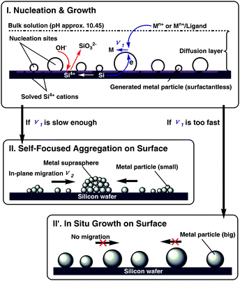 | ||
| Fig. 2 Schematic illustration of the formation mechanism of silicon-supported noble metal NP superstructures. (I) Nucleation and growth. The metal ions or metal–ligand precursors are nucleated on the surface by silicon reduction (the reaction rate is ν1), and simultaneously the SiO32− is generated and released into the weak basic solution. The two modes for the following process depending on the comparison between ν1 and aggregation speed ν2. (II) If ν1 is slow enough, metal supraspheres with a certain size and good monodispersity are finally formed. (II′) If ν1 is too fast, metal particles with larger size are finally formed. | ||
Further study revealed that if there were rubbing grooves on the silicon surface, the generated Ag NP superstructures were strictly localized in the “patterns” and the intact parts on the silicon surface were strongly screened, i.e., few Ag aggregates were formed (Fig. 3 and Fig. S8†). The scratching exposes the underlying silicon covered by the naturally oxidized layer, where Ag NP superstructures are easily produced via reduction. In addition, the arrangement of Ag NP superstructures can be manipulated by simple chemical pretreatment of the substrates. For example, the structures formed on the rubbing surface pretreated by HF acid (40%, 2 h) are stick-like Ag NP suprawires (SWs) (Fig. 3a–c), whereas necklace-like Ag SS assemblies are prepared on the rubbing surface without HF acid pretreatment (Fig. 3d–f). This observation highlights the possibility of not only positioning Ag NP superstructures but also tuning the inner fine structure.
 | ||
| Fig. 3 Ag NP superstructures formed on silicon wafers with rubbing grooves. (a–c) Stick-like Ag SWs obtained on the silicon wafer pretreated with HF acid (40%/2 h). (d–f) Necklace-like Ag SS assemblies obtained on the silicon wafer without HF acid pretreatment. The white arrows in (a) and (d) denote the rubbing direction. | ||
Based on the above observation, we used EBL and RIE to controllably design patterns on silicon wafers (Fig. 4a and Table S2†). By this technique, the naturally oxidized layer on the silicon surface was selectively removed and the Ag NP superstructures were expected to be preferentially generated in the patterns. Here, a 3 × 3 array in a 400 μm × 400 μm square area is fabricated (Fig. 4b). For each sub-array, it is composed of 1 × 10 etched lines, the width and length of the lines are 1 μm and 100 μm, respectively, and the space between the adjacent lines is 10 μm. It is evident that large-scale Ag NP superstructures with regular patterns are successfully prepared on the substrate (Fig. 4c–e). Interestingly, Ag SSs prefer growing and interconnecting to form Ag SWs along both edges of the etched lines due to the high surface energy of the edges. As a result, a parallel pair of Ag SWs with uniform width of about 300 nm appears in each etched line (Fig. 4f).
 | ||
| Fig. 4 2D patterned Ag NP superstructures formed on silicon wafers with etched line arrays. (a) Schematic illustration of the EBL-RIE-combined surface patterning and Ag NP formation process. (b) Optical image of the patterned silicon wafer with a 3 × 3 array. The black frame represents the selected sub-array corresponding to the SEM images in (c–f). Parts I–V are the five randomly selected locations for Raman characterization in Fig. 5d. (c) SEM image of the selected sub-array composed of 1 × 10 etched lines. The lines are 100 μm long and 1 μm wide, and the inter-spaces between the adjacent lines are 10 μm. (d) Magnified image of the Ag SWs generated in the etched lines. Each line contains two parallel Ag SWs. (e) Further magnified image of the two Ag SWs in one etched line. The space between the two SWs is about 500 nm. It reveals that the SWs preferentially grow along the two edges of the etched line. (f) A close-up image of the Ag NPs in one SW. The width of Ag SWs is consistent with dSS of single Ag SSs (about 300 nm). | ||
The dependence of the structures of Ag SWs on the etched line width was further studied in detail (Fig. S9†). Two types of etched line were designed: in Type I the line width (dline) is larger than double dSS of Ag SS and meanwhile in Type II dline is smaller than dSS. In Type I, Ag SWs preferentially grow along the edges of the etched line (Fig. S9a–f†), consistent with the result shown in Fig. 4. In Type II, Ag SWs preferentially grow along the central axis of the etched line (Fig. S9g–l†). By taking advantage of this growth feature, one can prepare small-size nanostructures from large patterns. For instance, two parallel Ag SWs with a space of 100 nm are easily realized in an etched line about 700 nm wide (Fig. S9†). This will greatly facilitate the patterning process and promote the efficiency of top-down fabrication.
Finally, the unique optical properties of the Ag NP superstructures were investigated. The scattering images and spectra of individual Ag SS and SW were acquired using a dark-field microscopy system with a true-color imaging charge-coupled device (CCD) camera and a spectrometer (Fig. 5a, b). The scattering peak of Ag SS is centered at 558 nm with full width at half maximum (FWHM) of about 110 nm. For Ag SW, the peak is at 565 nm with FWHM of also about 110 nm, and the slight red shift of the peak can be ascribed to one-dimensional optical coupling of Ag NPs in SWs. Notably, the scattering signals along the Ag SW are very uniform and no obvious color difference is observed either in the same SW or between different SWs (Fig. 5b). The optical properties of the Ag NP superstructures can be further used for highly sensitive SERS detection. One drop of PATP solution with ultralow concentration (100 μL, 10−10 M) was placed on the silicon wafer with Ag SW arrays and the sample was excited using a ∼2 mW 633 nm laser. No noticeable Raman signals are observed from the blank silicon surface without the Ag NP superstructures (Fig. 5c). The Raman spectra from single etched lines with Ag SWs I–V (marked in Fig. 4b) clearly exhibit the main vibrational features of PATP molecules (1080 cm−1: νCS + νCC; 1140 cm−1: βC–H; 1185 cm−1: βC–H; 1387 cm−1: βC–H + νCC; 1434 cm−1: νCC + βC–H; 1581 cm−1: νCC). It should be noted that these five Ag NP-decorated lines are randomly chosen and detectable SERS signals are highly reproducible with very similar strengths. Moreover, the high SERS sensitivity (10−10 M of PATP) on the Ag SWs is similar to or surpasses that in previous reports.39 As a comparison, the SERS signal from an individual Ag NP substrate obtained by reduction of Ag+/GSH complex precursors on a silicon wafer is much weaker, which is about ten times less than that on the Ag SS substrate (Fig. S10†). It further reveals the importance of close-packing Ag NP units in the superstructures, which can provide more “hot spots” and thus be a superior platform for ultrasensitive chemical detection.
 | ||
| Fig. 5 Optical characterization of the Ag NP superstructures on silicon substrates. (a) Dark-field scattering image of Ag SSs. Inset is the corresponding scattering spectrum of a single Ag SS. (b) Dark-field scattering image and the corresponding scattering spectrum (inset) of Ag SWs. (c) Raman spectrum collected from the blank silicon surface without Ag NP superstructures. (d) Raman spectra collected from the five randomly selected sample locations on the arrayed Ag SWs as marked in Fig. 4b. The detected molecules are PATP (10−10 M). The dashed lines denote the main vibrational peaks of PATP centered at 1080, 1140, 1185, 1387, 1434, and 1581 cm−1. | ||
In conclusion, by combining top-down fabrication and bottom-up self-assembly, 2D patterned Ag NP superstructures were successfully prepared on silicon wafers. This novel approach provides a unique and facile control over close-packing of Ag NP units inside the superstructures and the spatial arrangement of Ag NP superstructures on the substrates from nanoscale to macroscale. The patterned Ag NP superstructures show remarkably high and reproducible SERS enhancement and could be promising candidates for integrated design of multifunctional detecting chips, e.g. integration with nanoelectronics, nanophotonics and microfluidic channels.40–42
We thank the National High-Tech Research and Development Program (2007AA03Z302, Z. Y. T.), the 100-Talent Program of Chinese Academy of Sciences (Z. Y. T.), the National Science Foundation of China (20973047, Z. Y. T.), and the National Research Fund for Fundamental Key Project (2009CB930401, Z. Y. T.) for financial support of this research.
Notes and references
- S. A. Maier, Nat. Mater., 2009, 8, 699 CrossRef CAS.
- M. Aizawa and J. M. Buriak, J. Am. Chem. Soc., 2006, 128, 5877 CrossRef CAS.
- F. K. Liu, P. W. Huang, Y. C. Chang, F. H. Ko and T. C. Chu, Langmuir, 2005, 21, 2519 CrossRef CAS.
- C. Fang, A. Agarwal, H. Ji, W. Y. Karen and L. Yobas, Nanotechnology, 2009, 20, 405604 CrossRef CAS.
- A. K. Kalkan and S. J. Fonash, J. Phys. Chem. B, 2005, 109, 20779 CrossRef CAS.
- J. H. He and T. Kunitake, Langmuir, 2006, 22, 7881 CrossRef CAS.
- H. Zhang, R. C. Jin and C. A. Mirkin, Nano Lett., 2004, 4, 1493 CrossRef CAS.
- G. Zhang and D. Y. Wang, J. Am. Chem. Soc., 2008, 130, 5616 CrossRef CAS.
- L. Jiang, W. C. Wang, H. Fuchs and L. F. Chi, Small, 2009, 5, 2819 CrossRef CAS.
- H. Mertens, J. S. Biteen, H. A. Atwater and A. Polman, Nano Lett., 2006, 6, 2622 CrossRef CAS.
- H. Mertens, J. Verhoeven, A. Polman and F. D. Tichelaar, Appl. Phys. Lett., 2004, 85, 1317 CrossRef CAS.
- S. J. Huo, X. K. Xue, Q. X. Li, S. F. Xu and W. B. Cai, J. Phys. Chem. B, 2006, 110, 25721 CrossRef CAS.
- S. Patskovsky, A. V. Kabashin and M. Meunier, Opt. Mater., 2005, 27, 1093 CrossRef CAS.
- H. A. Atwater and A. Polman, Nat. Mater., 2010, 9, 205 CrossRef CAS.
- J. N. Anker, W. P. Hall, O. Lyandres, N. C. Shah, J. Zhao and R. P. Van Duyne, Nat. Mater., 2008, 7, 442 CrossRef CAS.
- A. V. Whitney, J. W. Elam, S. L. Zou, A. V. Zinovev, P. C. Stair, G. C. Schatz and R. P. Van Duyne, J. Phys. Chem. B, 2005, 109, 20522 CrossRef CAS.
- J. P. Camden, J. A. Dieringer, Y. M. Wang, D. J. Masiello, L. D. Marks, G. C. Schatz and R. P. Van Duyne, J. Am. Chem. Soc., 2008, 130, 12616 CrossRef CAS.
- J. Q. Gao, D. J. Liu and Z. X. Wang, Anal. Chem., 2008, 80, 8822 CrossRef CAS.
- M. Berger, Nano-Society: Pushing the Boundaries of Technology, CHAPTER 2 Building Nanostructures—from the Top Down and from the Bottom Up. RSC Nanoscience and Nanotechnology No. 8, 2009 Search PubMed.
- A. R. Tao, D. P. Ceperley, P. Sinsermsuksakul, A. R. Neureuther and P. D. Yang, Nano Lett., 2008, 8, 4033 CrossRef CAS.
- A. Tao, P. Sinsermsuksakul and P. D. Yang, Nat. Nanotechnol., 2007, 2, 435 CrossRef CAS.
- M. E. Stewart, C. R. Anderton, L. B. Thompson, J. Maria, S. K. Gray, J. A. Rogers and R. G. Nuzzo, Chem. Rev., 2008, 108, 494 CrossRef CAS.
- J. P. Camden, J. A. Dieringer, J. Zhao and R. P. Van Duyne, Acc. Chem. Res., 2008, 41, 1653 CrossRef CAS.
- B. Yan, A. Thubagere, W. R. Premasiri, L. D. Ziegler, L. D. Negro and B. M. Reinhard, ACS Nano, 2009, 3, 1190 CrossRef CAS.
- J. Zhao, A. O. Pinchuk, J. M. McMahon, S. Z. Li, L. K. Ausman, A. L. Atkinson and G. C. Schatz, Acc. Chem. Res., 2008, 41, 1710 CrossRef CAS.
- H. Wang, D. W. Brandl, P. Nordlander and N. J. Halas, Acc. Chem. Res., 2007, 40, 53 CrossRef CAS.
- A. Tao, P. Sinsermsuksakul and P. D. Yang, Angew. Chem., Int. Ed., 2006, 45, 4597 CrossRef CAS.
- B. Wiley, Y. G. Sun and Y. N. Xia, Acc. Chem. Res., 2007, 40, 1067 CrossRef CAS.
- X. M. Qian, X. Zhou and S. M. Nie, J. Am. Chem. Soc., 2008, 130, 14934 CrossRef.
- M. Labrenz, G. K. Druschel, T. T. Ebert, B. Gilbert, S. A. Welch, K. M. Kemner, G. A. Logan, R. E. Summons, G. D. Stasio, P. L. Bond, B. Lai, S. D. Kelly and J. F. Banfield, Science, 2000, 290, 1744 CrossRef CAS.
- F. Family, Kinetics of Aggregation and Gelation (Hardcover). North-Holland, 1985 Search PubMed.
- T. A. Witten and L. M. Sander, Phys. Rev. Lett., 1981, 47, 1400 CrossRef CAS.
- X. H. Sun, R. Sammynaiken, S. J. Naftel, Y. H. Tang, P. Zhang, P. S. Kim, T. K. Sham, X. H. Fan, Y. F. Zhang, C. S. Lee, S. T. Lee, N. B. Wong, Y. F. Hu and K. H. Tan, Chem. Mater., 2002, 14, 2519 CrossRef CAS.
- R. M. Stiger, S. Gorer, B. Craft and R. M. Penner, Langmuir, 1999, 15, 790 CrossRef CAS.
- S. G. Bratsch, J. Phys. Chem. Ref. Data, 1989, 18, 1 CrossRef CAS.
- Y. G. Sun and G. P. Wiederrecht, Small, 2007, 3, 1964 CrossRef CAS.
- Y. G. Sun, C. H. Lei, D. Gosztola and R. Haasch, Langmuir, 2008, 24, 11928 CrossRef CAS.
- C. Li, K. Deng, Z. Y. Tang and L. Jiang, J. Am. Chem. Soc., 2010, 132, 8202 CrossRef CAS.
- H. Y. Liang, Z. P. Li, W. Z. Wang, Y. S. Wu and H. X. Xu, Adv. Mater., 2009, 21, 4614 CrossRef CAS.
- M. J. Banholzer, J. E. Millstone, L. D. Qin and C. A. Mirkin, Chem. Soc. Rev., 2008, 37, 885 RSC.
- L. M. Liz-Marzán, Langmuir, 2006, 22, 32 CrossRef CAS.
- W. Chen, A. Bian, A. Agarwal, L. Q. Liu, H. B. Shen, L. B. Wang, C. L. Xu and N. A. Kotov, Nano Lett., 2009, 9, 2153 CrossRef CAS.
Footnote |
| † Electronic supplementary information (ESI) available: Experimental methods, additional experimental data. See DOI: 10.1039/c0jm02147d |
| This journal is © The Royal Society of Chemistry 2010 |