Interface engineering of organic electronics
The field of organic or plastic electronics originated in the 1950s with the discovery of electroluminescent organic molecules and the subsequent realization that organic molecules can also act as electrical conductors. In 1976, Alan MacDiarmid, Hideki Shirakawa and Alan Heeger were the first to discover conducting polymers and found that these polymers can be doped over the full range from insulator to metal.1 Early research on π-conjugated semiconducting and metallic polymers provided insight into the fundamental chemistry and physics of π-bonded macromolecules. These investigations also offered the promise of a new generation of unique polymeric materials that merge the electrical and optical properties of metals or semiconductors with the low cost, ease of processing, low weight, mechanical flexibility and versatility in the chemical design and synthesis of plastics.Among the most promising organic electronic devices are organic light-emitting diodes (OLEDs), field-effect transistors (OFETs), photovoltaic cells (OPVs) and memory. OLEDs have received much attention following the pioneering work of Tang and van Slyke in 19872 and Burroughes et al. in 1990.3 Around the same time, there was increasing interest in utilizing organic semiconductors in all-electrical processes for diodes and field-effect transistors.4 Since the 1990s, OLEDs, OFETs and OPVs have been extensively studied using molecular and polymeric systems and are now considered to be viable technologies for large-area flexible electronics.
With the continuous increase of OLED device efficiency and lifetime, OLED-based commercial products (e.g. small displays used in mp3-players, mobile phones, and car radios) are becoming progressively more economically feasible. Displays and lighting are two major applications of OLEDs in which the organic technology has the potential to compete with conventional technologies. However, light output, color, efficiency, cost, and lifetime of OLEDs need to be improved before commercial applications are practical.
Serving as the basis for integrated circuits, FETs are ubiquitous and are arguably one of the most crucial components of modern semiconducting technologies. Although inorganic FETs have been widely studied and implemented, OFETs are a relatively new field of research. Because of this, OFET device performance is not yet comparable to inorganic FET devices. However, once these operational issues are resolved, OFET technology could facilitate the production of inexpensive integrated circuits that would revolutionize widely used products like “smart” cards, audio amplifiers, large-area sensor arrays and radiofrequency frequency identification (RFID) tags. In addition, OFETs can form backplane circuitry for active-matrix liquid crystal displays (AMLCD).
An organic approach to photovoltaics could also yield similar benefits. PV technology can be a major contributor to renewable energy production and a realistic solution to energy scarcity problems. Despite the fact that a superfluous amount of solar energy is available to power all human activities, solar energy only accounts for a small percentage of our energy production. Largely, this is because PV technology is prohibitively expensive. With improvements in device performance, OPV technology can possibly become more economically feasible because it is cheaper to synthesize and manufacture than inorganic PV devices and solution-processed OPV can potentially be mass-produced in large-scale printing processes. Also, OPV can possibly be integrated into everyday items like automobiles, clothing and handheld electronics. However, the overwhelming number of possibilities for material synthesis is an obstacle to realization of these applications.
The performance and lifetime of organic electronic devices are critically dependent on the properties of both the active materials and their interfaces. In these devices, metal electrodes are utilized to inject charge into (or extract charge from) the organic semiconductor layer(s). Therefore, control over the interface between organic semiconductor and inorganic electrode/dielectric is essential. This can range from simple wettability or adhesion between different materials to direct modification of the electronic structure of the material. For instance, factors such as the surface energy and work function greatly affect the charge injection/extraction and transport in organic semiconductors.
Although developing new conjugated materials can tune the emission color, electron affinity, and charge mobility of the OLED, interfacial modification between organic semiconductors and inorganic electrodes is critical to optimize charge injection, transport, and recombination and, ultimately, to improve OLED performance. Fundamentally understanding the physical properties of the intermediate connectors in tandem OLEDs is crucial to improve our understanding of device mechanics and to develop high-efficiency tandem organic (opto)electronic devices. In this issue, the working mechanisms of several effective intermediate connectors in tandem OLEDs using doped or non-doped organic p–n heterojunctions are presented by Lee et al. (DOI: 10.1039/b921699e; Fig. 1).
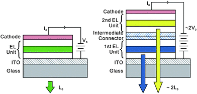 | ||
| Fig. 1 From Lee et al. (DOI: 10.1039/b921699e). | ||
So far, the most efficient polymeric solar cells (PSCs) are based on the bulk heterojunction (BHJ) architecture prepared by mixing electron-rich polymers and electron-deficient fullerides. PSCs generate power through three major processes: exciton generation (absorption), charge separation (the process of excitons migrating to the donor/acceptor interface and being split into their constituent charges), and charge transport. Thus it is essential to control charge transfer and carrier recombination across donor/acceptor interfaces in a BHJ structure. Contact resistance between layers must be minimized to reduce the device series resistance, which is important in maximizing the fill factor and PSC efficiency. Moreover, physical properties such as wetting between organic and inorganic components and adhesion between layers are important for device performance and lifetime. Encouragingly, interface engineering can passivate charge trap states, control energy level alignment, enhance charge extraction, guide active layer morphology, improve materials compatibility, alter work functions of both anode and cathode to optimize open circuit voltage, and ultimately allow the fabrication of high-efficiency OPV cells. Theoretical study of the surface modification and interfacial tailoring of anode and cathode is reported by Bredas et al. (DOI: 10.1039/b921768a), Armstrong et al. (DOI: 10.1039/b923201j), and Bazan, Cao and coworkers (DOI: 10.1039/b921775d). The progress of interface engineering in PSCs is summarized in the feature article by Yang et al. (DOI: 10.1039/b925382c).
Similarly, OFET interfaces also play a crucial role in overall performance: the source/drain metal electrode/organic semiconductor interface influences charge carrier injection, while the gate insulator/organic semiconductor interface is important for the formation—or interruption—of a conducting channel. The control of interfacial morphologies and energetics by utilizing self-assembled monolayers (SAMs) is reviewed in the feature article by Horowitz et al. (DOI: 10.1039/b922385a; Fig. 2). The effect of a SAM-modified dielectric interface on OFET performance is reported by Bao et al. (DOI: 10.1039/b921767c) and Im et al. (DOI: 10.1039/b921636g). Two review articles (by Liu et al. (DOI: 10.1039/b921449f; Fig. 3) and Cho et al. (DOI: 10.1039/b924415h)) highlight recent progress on engineering the dielectric/semiconductor interface and its dramatic effects on the morphology and charge-transport of organic semiconductors in OFETs. A highlight article by Samori et al. (DOI: 10.1039/b921612j), and an article by Malliaras et al. (DOI: 10.1039/b923375j) discuss the formation of suprastructures during macroscopic healing of molecular assemblies and provide valuable novel insight into the solvent vapor annealing process. FET sensing with various semiconductor materials and receptor functionality is reported in a paper by Katz et al. (DOI: 10.1039/b916037j). Interface tailored FET memory is discussed in the paper by Im and coworkers (DOI: 10.1039/b921732k).
 | ||
| Fig. 2 From Horowitz et al. (DOI: 10.1039/b922385a). | ||
 | ||
| Fig. 3 From Liu et al. (DOI: 10.1039/b921449f). | ||
By integrating the excellent works related to interface engineering from leading experts in the field, we hope this thematic issue will become a useful reference for readers who have interest in developing materials and devices for diverse applications in the broadly defined organic electronics.
 | ||
| Plate1 Alex K.-Y. Jen, Department of Materials Science & Engineering, University of Washington | ||
References
- H. Shirakawa, E. J. Louis, A. G. MacDiarmid, C. K. Chiang and A. J. Heeger, J. Chem. Soc., Chem. Commun., 1977, 578 RSC.
- C. W. Tang and S. A. Van Slyke, Appl. Phys. Lett., 1987, 51, 913 CrossRef CAS.
- J. H. Burroughes, D. D. C. Bradley, A. R. Brown, R. N. Marks, K. Mackey, R. H. Friend, P. L. Burn and A. B. Holmes, Nature, 1990, 347, 539 CrossRef CAS.
- J. H. Burroughes, C. A. Jones and R. H. Friend, Nature, 1988, 335(6186), 137 CrossRef.
| This journal is © The Royal Society of Chemistry 2010 |