Lithography-free production of stamps for microcontact printing of arrays
Rahul
Thakar
and
Lane A.
Baker
*
Department of Chemistry, Indiana University, 800 E. Kirkwood Avenue, Bloomington, IN 47405, USA. E-mail: lanbaker@indiana.edu
First published on 4th June 2010
Abstract
A simple method for fabricating polydimethylsiloxane (PDMS) stamps suitable for microcontact printing applications is described. The method makes use of Formvar®-coated grids used for electron microscopy and requires no photolithography or advanced processing techniques. Utilization of fabricated stamps in microcontact printing and in electrochemical microscopy is described.
Microcontact printing (µCP) has proven to be a highly versatile method for micro- and nanofabrication.1–4 In a common implementation of µCP, a micropatterned polymer stamp is first fabricated from PDMS. A solution of molecules is then placed onto the stamp and the solution is allowed to evaporate, leaving behind a thin layer of molecules. When the PDMS stamp is subsequently pressed into intimate contact with a substrate of interest, molecules from the stamp are transferred to the substrate, creating a pattern on the substrate that is a replica of the stamp. While conceptually simple, this technique has found wide application in microfabrication and has become an indispensable tool for many analytical and bioanalytical applications, especially for the generation of patterned surfaces. For example, surfaces patterned with alkanethiols, siloxanes, metals, nanoparticles, proteins, viruses, and cells have all been realized using µCP.5–11 A number of advances including submicron resolution12,13 and stamp materials with improved viscoelastic properties have further advanced the capabilities of µCP.14 Applications of µCP extend beyond patterning of surfaces to a number of venues which have been described in recent reviews.1,2,8,15,16 In this technical note we detail an extremely simple method to prepare stamps for microcontact printing that does not rely on photolithography and can be implemented without the use of any specialized equipment. The method is especially well-suited to preparing µCP stamps for the formation of arrays directly from transmission electron microscopy grids, but could be extended to other porous masters as well.
The first step in µCP is the fabrication of a suitable stamp. The most common method to fabricate the stamp is photolithography.2,17 In this method a photoresist is coated onto a flat surface, such as a silicon wafer. A pattern is then transferred to the resist using photolithography, creating a master. A negative stamp of the resist pattern is then created by pouring uncured PDMS over the stamp and allowing the polymer to cure. Peeling the PDMS off of the resist master gives a three-dimensionally patterned stamp. Other methods to fabricate stamps, such as injection molding, have also been described.18,19 Most stamp preparation methods require some level of lithographic or moderately advanced microfabrication technique which can prove expensive in capital and operating costs, and are not always readily available. The simple method we describe herein is particularly cost-effective (∼$1 (US) per grid) and is carried out on laboratory bench-tops eliminating the need of clean room facilities.
First, step (a), a copper or gold transmission electron microscopy grid is acquired and a thin Formvar® film is adhered to the surface (see experimental).20 This practice is commonly used to prepare grids for electron microscopy where small samples rest on top of the support film during imaging.21 For this purpose, Formvar® (polyvinyl formal) or Butvar (polyvinyl butyral) are commonly used films owing to their rigidity. Other commonly used support films include holey carbon and silicon nitride. Formvar® film forms a “top” or a capping layer on one side of the TEM grid. In practice the films applied are ∼25 to 30 nm in thickness. Precoated grids can also be obtained, which simplifies the procedure even further by omitting step (a). The Formvar®-coated grid is then placed with the Formvar® side facing the bottom of a Petri dish and uncured PDMS is poured over the top of the grid (step (b)). The sample is evacuated to remove air bubbles, and the PDMS is cured at 85 °C for 2 hours. Under microscopic observation, a PDMS block surrounding the grid is then cut out from the dish (step (c)), and the grid is carefully peeled from the PDMS block, leaving a replica of the original grid (Fig. 1). Due to fragile nature of TEM grids they can break or tear during this process, therefore it is recommended that a new TEM grid (Formvar®-coated) is used each time a stamp is fabricated. In the absence of a Formvar® coating PDMS seeps under the grid and simply encases the grid. The presence of Formvar® forms a bottom to each hole in the grid, effectively creating a microwell. Adhesion of the Formvar® to the grid and the mechanical properties of Formvar® prove sufficient to withstand the mild processing conditions employed here.
 | ||
| Fig. 1 Schematic for µCP stamp formation. (a) Transmission electron microscopy grid is coated with a layer of Formvar®; (b) PDMS is poured on top of the grid and cured; (c) grid is excised from cured PDMS and removed, leaving replica in PDMS stamp. | ||
Grids with mesh sizes from 10–50 microns in size were examined, with results reported in Table 1. Grid hole sizes (reported by the manufacturer) are reported for each mesh size, and the corresponding size of each hole of the TEM grid (measured by electron microscopy) is reported. The size of each feature produced in the PDMS stamps (measured by electron microscopy) is also shown. In general, the feature size reproduces the TEM-grid master with good fidelity (>95% confidence). In the case of 600 mesh grids, the TEM-grid master has grid shapes that are intrinsically irregular in shape (leading to greater deviation in feature size), which is replicated in the PDMS stamp. Electron micrographs of µCP stamps prepared from 600 mesh and 1000 mesh grids are displayed in Fig. 2. In Fig. 2a, a plan view of a µCP stamp from the 600 mesh master shows irregularly sized features that reproduce the pattern of the original master well (for masters used, only the 600 mesh displayed this irregularity in size). In Fig. 2b, a tilted perspective of a µCP stamp from the 1000 mesh master demonstrates the long range order achievable with this simple procedure.
| Mesh size | Grid hole size/µm | TEM grid size/µm | PDMS stamp feature size/µm |
|---|---|---|---|
| a n > 25. b Obtained from the manufacturer website (Ted Pella). c Refers to the grid hole but features obtained include an edge defect which increases the size of the actual grid size. | |||
| 400 | 42c | 49.65 ± 0.31 | 47.24 ± 0.47 |
| 600 | 37 | 25.74 ± 2.08 | 26.03 ± 1.66 |
| 1000 | 19 | 18.69 ± 0.13 | 18.52 ± 0.23 |
| 1500 | 11.5 | 10.42 ± 0.30 | 10.16 ± 0.21 |
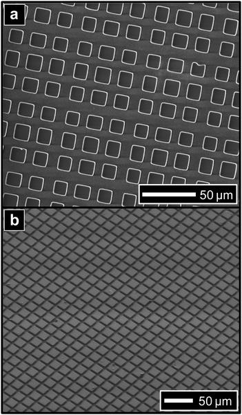 | ||
| Fig. 2 Electron micrographs of PDMS µCP stamps prepared from transmission electron microscopy grids. (a) Plan view of stamp prepared from 600 mesh grid; (b) tilted perspective view of stamp prepared from 1000 mesh grid. | ||
Utilization of µCP stamps prepared in this manner was also investigated. PDMS stamps themselves prove to be an excellent substrate for assessing micro- and nanoelectrodes applied to scanning electrochemical microscopy (SECM).22 The raised features of the stamp provide a non-conductive feature that is soft and pliable. When immersed in a solution of redox mediator, the trenches between features fill with solution. When an electrode is approached over a feature in the stamp, negative feedback of the redox mediator results from the small separation between tip and sample, and is recorded as a depression in faradaic current. Scanning the tip off of the feature, over a solution-filled trench results in an increase in current that rises from redox mediator present in solution. An image recorded in this manner is shown in Fig. 3a for a PDMS stamp prepared from a 400 mesh grid. The relatively soft material properties of PDMS in this application prove especially valuable when evaluating the performance of small nanoelectrode SECM tips operated in constant-height mode, where tip-sample separations are small and the electrodes can be extremely fragile. Thus the PDMS stamp provides an easily prepared, well-characterized substrate that can serve to minimize electrode damage.
 | ||
| Fig. 3 Application of PDMS stamps prepared. (a) Scanning electrochemical micrograph of a PDMS stamp. PDMS features show up as nonconducting regions, trenches show up as conducting regions (note: slope in the image results from SECM measurement, not the PDMS stamp); (b) scanning electron micrograph of an array of gold squares formed by µCP of thiol and subsequent chemical etching. See text for experimental details. | ||
A second application of PDMS stamps using µCP is shown in Fig. 3b. Initially, a gold film was deposited on a glass slide. Inking a PDMS stamp with hexadecane thiol followed by pattern transfer of the thiol ink to the gold-coated slide results in a pattern of hexadecane thiol on the gold substrate. Subsequent chemical etching of the surface results in removal of gold from noncontacted regions of the surface and protection from chemical etching in regions that were stamped. Unprotected gold was cleanly removed and fidelity in pattern transfer was high. This example demonstrates that µCP stamps prepared as described here function in a manner analogous to stamps prepared using traditional photolithography.3,23–25
Conclusions
We have demonstrated a simple approach to the formation of PDMS stamps suitable for µCP applications. Coating of a porous substrate (TEM grid) with Formvar® produces a master that can be used for stamp formation without the need for photolithography or complicated processing. Application of stamps as reference metrics for SECM and in formation of gold island arrays was used to demonstrate utility of prepared stamps. We expect this extremely simple method will further extend the reach of µCP and could find application in undergraduate teaching laboratories as well as in research settings.Experimental
Chemical and materials
All chemicals were obtained and used as received without further purification. Aqueous solutions were prepared in 18 MΩ cm H2O from a Milli-Q water purification system (Millipore Corp., Danvers, MA). Gold etching solution was a mixture of 20 mM thiourea, 30 mM iron nitrate, 20 mM hydrochloric acid and 20 mM octanol. Sylgard 184 PDMS elastomer kit was obtained from Dow Corning (MI).Formation of PDMS stamps
Formvar®-coated Cu-400 mesh (01754-F) and transmission electron microscopy (TEM) grids (Ted Pella, Redding, CA) were used as received. Cu-600 (G600HSS), Cu-1000 (G1000HS) and Cu-1500 (G1500HS) mesh TEM grids (Ted Pella, Redding, CA) were treated with 0.25% Formvar® solution in ethylene dichloride (Electron Microscopy Sciences, Hatfield, PA) to apply a film of Formvar®.20 On application of Formvar® coating on the shiny side (referred to as the top side) of TEM grids, they were left to dry overnight. Commercially obtained Formvar® grids (400 mesh) were more than a month old and all the other grid sizes (600, 1000, 1500 mesh) to which Formvar® was applied were used within a week of applying. Formvar® TEM grids were placed in a Petri dish with the Formvar®-coated side facing downwards. Prepolymer and curing agent were manually mixed in a 10 : 1 volume ratio and poured over the TEM grid. The Petri dish was placed inside a vacuum chamber to dispel air bubbles from the elastomer. PDMS was then cured in an oven at 85 °C for two hours. Stamps were cut out of the PDMS block and the copper TEM grid was gently peeled off under a microscope. Prepared PDMS stamps and commercially obtained TEM grids were characterized using a scanning electron microscope (Quanta-FEG, FEI).Scanning electrochemical microscopy of PDMS stamp
Imaging of 400 mesh PDMS stamps was performed using a commercial SECM instrument, model 910B (CH instruments, TX). A polished platinum working electrode fabricated using a pipette puller was used for imaging in constant-height, negative feedback mode. A AgCl coated Ag wire served as a reference electrode and a platinum wire (0.5 mm diameter) was used as a counter electrode. An aqueous solution of 10 mM potassium ferricyanide (Darmstadt, Germany) solution was used as redox mediator containing 1 M potassium chloride (Mallinckrodt, Philipsburg, NJ) as the supporting electrolyte.Microcontact printing of 1-hexadecanethiol on gold slides and subsequent chemical etching26
Glass slides were soaked in 1 : 3 volume ratio of H2O2/H2SO4 solution for at least an hour and thoroughly rinsed with 18 MΩ H2O, ethanol and dried under a stream of nitrogen. Cleaned glass slides were used for depositing chromium as the adhesion layer followed by gold deposition inside a thermal evaporator. All procedures were performed in the clean room and samples were saved for use within a week. A Cu-400 mesh, PDMS stamp was soaked in a freshly prepared ethanolic solution of 2 mM 1-hexadecanethiol (97%) (Alfa-Aesar, Ward Hill, MA). Stamps were washed in ethanol, dried under a stream of nitrogen and placed in contact with gold coated slides for over 1 minute to transfer thiol molecules. Gold coated samples were washed in ethanol, dried under nitrogen and immersed in a gold etching solution. In order to avoid excessive etching, samples were monitored under a microscope periodically. Patterned and etched samples prepared using this procedure were washed in ethanol, dried in nitrogen and characterized with scanning electron microscopy.Notes and references
- Z. Fan, J. C. Ho, T. Takahashi, R. Yerushalmi, K. Takei, A. C. Ford, Y.-L. Chueh and A. Javey, Adv. Mater., 2009, 21, 3730 CrossRef CAS.
- D. Qin, Y. Xia and G. M. Whitesides, Nat. Protocol., 2010, 5, 491 Search PubMed.
- J. L. Wilbur, A. Kumar, H. A. Biebuyck, E. Kim and G. M. Whitesides, Nanotechnology, 1996, 7, 452 CrossRef CAS.
- S. A. Ruiz and C. S. Chen, Soft Matter, 2007, 3, 168 RSC.
- D. Qin, Y. Xia, B. Xu, H. Yang, C. Zhu and G. M. Whitesides, Adv. Mater., 1999, 11, 1433 CrossRef CAS.
- W. M. Lackowski, P. Ghosh and R. M. Crooks, J. Am. Chem. Soc., 1999, 121, 1419 CrossRef CAS.
- K. Godula, D. Rabuka, K. T. Nam and C. R. Bertozzi, Angew. Chem., Int. Ed., 2009, 48, 4973 CrossRef CAS.
- D. B. Weibel, W. R. DiLuzio and G. M. Whitesides, Nat. Rev. Microbiol., 2007, 5, 209 Search PubMed.
- R. S. Kane, S. Takayama, E. Ostuni, D. E. Ingber and G. M. Whitesides, Biomaterials, 1999, 20, 2363 CrossRef.
- J. Noo Li, I. S. Choi, G. M. Whitesides, N. Y. Kim, P. E. Laibinis, Y. Harada, K. R. Finnie, G. S. Girolami and R. G. Nuzzo, Appl. Phys. Lett., 1999, 75, 4201 CrossRef CAS.
- D. J. Solis, S. R. Coyer, A. J. García and E. Delamarche, Adv. Mater., 2010, 22, 111 CrossRef CAS.
- T. Pompe, A. Fery, S. Herminghaus, A. Kriele, H. Lorenz and J. P. Kotthaus, Langmuir, 1999, 15, 2398 CrossRef CAS.
- D. M. Longo, W. E. Benson, T. Chraska and R. Hull, Appl. Phys. Lett., 2001, 78, 981 CrossRef CAS.
- R. Mukhopadhyay, Anal. Chem., 2007, 79, 3248 CrossRef CAS.
- A. Perl, D. N. Reinhoudt and J. Huskens, Adv. Mater., 2009, 21, 2257 CrossRef CAS.
- B. J. Ravoo, J. Mater. Chem., 2009, 19, 8902 RSC.
- Z. Nie and E. Kumacheva, Nat. Mater., 2008, 7, 277 CrossRef CAS.
- A. Chandekar, M. Alabran, S. K. Sengupta, J. S. Lee, J. L. Mead, C. M. F. Barry, J. E. Whitten, S. Somu and A. A. Busnaina, Microelectron. Eng., 2008, 85, 187 CrossRef CAS.
- G. Jing, J. P. Labukas, W. Zhang, S. F. Perry, S.-F. Lu, G. S. Ferguson and S. Tatic-Lucic, Microelectron. Eng., 2009, 86, 2334 CrossRef CAS.
- I. Shore and J. Moss, Histochem. J., 1988, 20, 183 CrossRef CAS.
- D. B. Nowak, M. K. Vattipalli, J. J. Abramson and E. J. Sánchez, J. Microsc., 2008, 230, 32 CrossRef CAS.
- H. Shiku, T. Saito, C.-C. Wu, T. Yasukawa, M. Yokoo, H. Abe, T. Matsue and H. Yamada, Chem. Lett., 2006, 35, 234 CrossRef CAS.
- A. Kumar, H. A. Biebuyck and G. M. Whitesides, Langmuir, 1994, 10, 1498 CrossRef CAS.
- Y. Xia and G. M. Whitesides, Annu. Rev. Mater. Sci., 1998, 28, 153 CrossRef CAS.
- T. K. Whidden, D. K. Ferry, M. N. Kozicki, E. Kim, A. Kumar, J. Wilbur and G. M. Whitesides, Nanotechnology, 1996, 7, 447 CrossRef CAS.
- Z. Zheng, J.-W. Jang, G. Zheng and C. A. Mirkin, Angew. Chem., Int. Ed., 2008, 47, 9951 CrossRef CAS.
| This journal is © The Royal Society of Chemistry 2010 |