Carbon nanotube-based organic light emitting diodes
Malti
Bansal
*a,
Ritu
Srivastava
b,
C.
Lal
c,
M. N.
Kamalasanan
b and
L. S.
Tanwar
a
aDepartment of Physics, School of Applied Sciences, Netaji Subhas Institute of Technology, Sector-3, Dwarka, New Delhi 110075, India. E-mail: maltibansal@gmail.com
bCentre for Organic Electronics, National Physical Laboratory (Council of Scientific and Industrial Research), Dr K. S. Krishnan Road, New Delhi 110012, India
cCarbon Technology Unit, National Physical Laboratory (Council of Scientific and Industrial Research), Dr. K. S. Krishnan Road, New Delhi 110012, India
First published on 5th October 2009
Abstract
Carbon nanotubes; revolutionary and fascinating from the materials point of view and exceedingly sensational from a research point of view; are standing today at the threshold between inorganic electronics and organic electronics and posing a serious challenge to the big daddies of these two domains in electronics i.e., silicon and indium tin oxide (ITO). In the field of inorganic electronics, carbon nanotubes offer advantages such as high current carrying capacity, ballistic transport, absence of dangling bonds, etc. and on the other hand, in the field of organic electronics, carbon nanotubes offer advantages such as high conductivity, high carrier mobility, optical transparency (in visible and IR spectral ranges), flexibility, robustness, environmental resistance, etc. and hence, they are seriously being considered as contenders to silicon and ITO. This review traces the origin of carbon nanotubes in the field of organic electronics (with emphasis on organic light emitting diodes ) and moves on to cover the latest advances in the field of carbon nanotube-based organic light emitting diodes . Topics that are covered within include applications of multi-wall nanotubes and single-wall nanotubes in organic light emitting diodes . Applications of carbon nanotubes as hole-transport layers, as electron-transport layers, as transparent electrodes, etc. in organic light emitting diodes are discussed and the daunting challenges facing this progressive field today are brought into the limelight.
 Malti Bansal | Malti Bansal received her BSc (Honours) Electronics Degree and MSc (Electronics) Degree from the University of Delhi, India in 2003 and 2005 respectively. Subsequently she was awarded a research fellowship from the Netaji Subhas Institute of Technology, India. She worked on the synthesis and characterization of silicon carbide nanomaterials and their applications in the field of nanocomposites. In May 2007, she started her Doctoral work in the field of carbon nanotubes and is currently pursuing the same at the National Physical Laboratory, India and the Netaji Subhas Institute of Technology, India. Her current research interests include synthesis of carbon nanotubes, their characterization and applications in the field of macroelectronics and nanoelectronics. |
1. Introduction
Carbon nanotube hysteria—a phenomenon which started with Sumio Iijima's miraculous rediscovery1 of these magical nanostructures in 1991 and blasted off a scientific typhoon, starting with the synthesis of carbon nanotubes, study of their properties, their characterization, and ultimately their applications in literally every known field. The field of organic electronics has also been engulfed in this tempest. In fact, the confluence of the two major giants (organic electronics and carbon nanotubes) has further enriched the electronics macrocosm with devices such as carbon nanotube-based organic light emitting diodes , carbon nanotube-based solar cells, carbon nanotube-based thin film transistors, etc. These devices have been found to exhibit comparable and in some cases superior properties as compared to their counterparts without carbon nanotubes, and without the associated disadvantages observed in their counterparts. This has lead to a blossoming of this novel field with unprecedented euphoria.In the field of organic electronics, carbon nanotubes are generally employed in the form of thin films of random networks of carbon nanotubes or what has come to be termed “carbon nanonets”52 and this has lead to the rapid emergence of carbon nanotube-based printed, plastic, disposable or macroelectronic products. Although, since their discovery, the emphasis in the field of electronics regarding carbon nanotubes has been on carbon nanotube-based nanoelectronics, it has been only recently that carbon nanotubes in the form of carbon nanonets have led to rebirth of “macroelectronics”. Carbon nanotubes, in the form of nanonets,52 lend themselves to solution-based fabrication techniques, such as room-temperature coating, printing (R2R processing techniques) or spraying technologies. Moreover, they offer excellent and tunable electrical, optical and mechanical properties and thus, bring the idea of large area, flexible, ultra-thin, low-weight, low-cost and high-throughput electronics closer to reality. According to market research firm iSuppli Corp., the flexible display market is expected to grow from $5 million in 2006 to $339 million in 2013, or 83.5 % per year.2 In such a scenario, carbon nanotubes look set to revolutionize the flexible display landscape in the near future, leaving old favourites like ITO, stainless steel, plastic, glass, etc., miles behind.
2. Carbon nanotubes and their flavours
Carbon nanotubes are hollow cylinders of graphite sheets (∼nm in diameter and ∼µm in length). Structurally, carbon nanotubes exhibit two flavours i.e., single-wall carbon nanotubes and multi-wall carbon nanotubes. A tube made of a single graphite layer rolled up into a hollow cylinder is called a single-wall nanotube (SWNT) whereas a tube comprising several, concentrically arranged cylinders is referred to as a multi-wall nanotube (MWNT) (Fig. 1).3Carbon nanotubes combine nanometric size with high aspect ratio (∼1000) and exhibit unique electrical, optical, mechanical and electrochemical properties,4–9 such as a high elastic modulus of 1–2 TPA, high electrical conductivity (about 1000 times higher than copper wire), high thermal conductivity (∼2000 W mK−1), etc. As such, they are ideal candidates for high-impact applications in diverse fields.10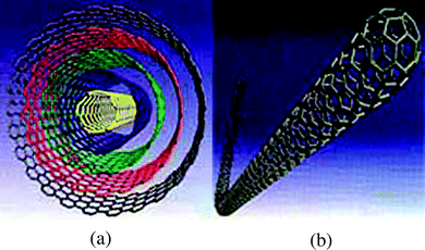 | ||
| Fig. 1 Graphic depicting (a) a multi-wall carbon nanotube and (b) a single-wall carbon nanotube (http://www.azonano.com). | ||
3. Multi-wall carbon nanotubes (MWNTs)
Multi-wall carbon nanotubes generally exhibit diameters from two to several hundred nanometres, lengths up to several microns and inter-tube spacing of around 0.34–0.35 nm. A carbon nanotube can be either a metal or a semiconductor , depending on how the tube is rolled up.11 However, it has been observed that generally single-wall nanotubes exist as mixtures of metallic and semiconducting tubes, whereas, owing to their larger diameter and more complex multi-layered structure, multiwall nanotubes are essentially metallic in nature.12,13 Moreover, MWNTs are slightly easier to process than SWNTs,14 because they are less prone to forming tight bundles. Also, because of the large number of concentric cylindrical graphitic tubes, MWNTs are perhaps even more suitable for achieving charge transfer and charge transport.143.1. Work function of MWNTs
Work function is a very important parameter when considering the design of carbon nanotube-based macroelectronic devices such as diodes, light emitting diodes and photovoltaic devices. As reported by Ago et al.,15,16 the work function of purified MWNTs (nanotube–water solution dispersed by non-ionic surfactant (Triton X-100)) using ultraviolet photoelectron spectroscopy (UPS) is 4.3 eV, air oxidation slightly increases the work function to 4.4 eV, oxygen-plasma treatment increases the work function to 4.8 eV and acid oxidation (in H2SO4 and HNO3) further raises the work function to 5.1 eV. Oxidation of MWNTs in air introduces mainly hydroxyl and carbonyl groups. Plasma treatment destroys the π-conjugation16 and forms an amorphous carbon phase (a fact important with respect to organic electronic devices) and acid oxidation introduces carboxylic acid groups on the surfaces of MWNTs.3.2. Applications of MWNTs in OLEDs
Multi-wall nanotubes have been employed in organic light emitting diodes (OLEDs) as hole-injecting electrodes, as charge-transport layers, etc.MWNTs are generally employed either in the form of a composites with conjugated polymers or as plain sheets, in OLEDsIn the case of composites, the concept of percolation and percolation threshold comes into the picture. Percolation is a statistical concept which describes the formation of conducting pathways in different dimensions, using objects of various geometries and falls under the realm of percolation theory.17–20 The percolation threshold is defined as the lowest filler concentration needed for a macroscopic conductivity increase i.e., formation of an electrical pathway through the sample.21 The technological importance of design near the percolation threshold for a composite is self-evident: selection of the minimum amount of filler material reduces cost and mass as well as preserving the intrinsic properties of the host material. Percolation strongly depends on the aspect ratio of the filler material particles. It has been shown experimentally, as well as theoretically, that the percolation thresholds decrease significantly as the aspect ratio of the filler particles increases.22 Here, carbon nanotubes with their large aspect ratio and high conductivity emerge as the most befitting candidate, for filler applications in composite materials. Nanotubes interact with the polymervia weak van der Waals interactions and hence, there is no decrease in stability of the composite as a result of the addition of nanotubes.23 Moreover, the addition of nanotubes to the polymer also increases its mechanical strength, thermal conductivity and optical stability apart from enhancement in electrical conductivity.23 The basic design route is the formation of MWNT-conjugated polymer composites and then casting of the composite films onto the required substrate (the substrate depends on the application of the composite; as the electrode or charge-transport layer in the OLED) using various methods.
Multifarious methodologies exist for depositing carbon nanotube composite thin films such as drop-casting from solvent,24 airbrushing or spray-coating,25,36 quasi-Langmuir–Blodgett deposition26 Langmuir–Blodgett deposition,27dip-coating,28vacuum filtration,29spin-coating,30 layer-by-layer coating,31 bar-coating,32 doctor-blade technique,33electrophoretic deposition,34 self-assembled monolayer technique,35 direct CVD growth on substrate,37 inkjet printing,38PDMS-based transfer-printing technique,39PDMS-based transfer-printing technique combined with vacuum filtration,40 line patterning method,41filtration-wet transfer process,42 controlled flocculation process combined with PDMS-based transfer-printing technique,43spin-coating combined with an applied magnetic field,44 drawing from a vertically oriented nanotube forest,67 wire-wound rod-coating,45,46 slot-coating47etc.—each with its own cheers and jeers. We will be not discussing these methodologies in detail here and rather move on to the application of MWNT-conjugated polymer composites in OLEDs.
The first attempt at utilizing MWNTs in OLEDs was reported by Romero et al.61 They fabricated a diode comprised of MWNTs and poly(2,5-bis(cholestanoxy)-1,4-phenylenevinylene) (BCHA-PPV) where the MWNT layer was used as the hole-injecting layer. The surface of the MWNTs was initially covered with a solution of BCHA-PPV in xylene under an over pressure of 2 atm of argon in order to allow the polymer to penetrate the spaces between the tubes. A final layer of the polymer was subsequently spin-cast onto the MWNT layer. A rectifying heterojunction was observed to be formed at the interface between the MWNT layer and BCHA-PPV and the hole-injection at this interface was achieved at much lower applied electric fields due to the enhancement of the local field at the tip of the nanotubes. No light emission was however observed from the MWNT/BCHA-PPV/Al device. This was probably due to the excessively thick polymer layer (BCHA-PPV) covering the carbon nanotube layer. Subsequently, Curran et al.62 prepared composites of MWNTs and poly(p-phenlyenevinylene-co-2,5-dioctoxy-m-phenylenevinylene) (PmPV) and observed an increase in electrical conductivity of up to eight orders of magnitude for very low concentrations of nanotubes. This was an encouraging result and a consequence of the high electrical conductivity of carbon nanotubes. Percolating networks were formed at very low carbon nanotube concentrations. It was suggested that the polymer, PmPV, owing to its helical structure, wraps itself around the nanotubes and keeps them suspended in solution indefinitely, thus solving the dispersion problem of carbon nanotubes. Hence, the composite was found to be an excellent combination, exhibiting the beneficial properties of both components, at very low filler concentration. However, the luminescence intensity was found to decrease due to the introduction of nanotubes. On the other hand, the rate of photobleaching of the polymer was dramatically decreased due to the incorporation of nanotubes. It was suggested that MWNTs act as nanometric heat sinks in the polymer matrix, dissipating the heat generated in the PmPV during operation. LEDs having the device configuration ITO/PmPV–MWNT composite/Al were fabricated and were reported to show lifetimes in air up to 5 times longer (at 5% MWNT mass fraction) than equivalent pristine polymer devices. Dalton et al.63 also prepared a MWNT–PmPV composite and showed that the quantum efficiency of the composite can be controlled by the concentration of nanotubes present. Moreover, it was suggested that the nanotubes are held in the polymer matrix through a weak interaction between the backbone of the polymer and the lattice of the nanotube. Thus, PmPV provides an ideal solution for dispersing nanotubes (a critical problem in preparing carbon nanotube-based composites) without altering the chemical structure of nanotubes. Coleman et al.23 investigated the percolation-dominated conductivity in PmPV–MWNT composites and found that the introduction of nanotubes (from low to high mass fractions (0.5–36%)) to the polymer increased its conductivity dramatically by ten orders of magnitude, again indicative of percolative behaviour (Fig. 2). The percolation threshold was obtained at approximately 8.5% mass fraction of carbon nanotubes. The current increase below 8% nanotube concentration was predicted to be due to the increased carrier (electron) donation by the nanotubes and the increase in partial conductive paths in the composite sample. The increase in current above 8% nanotube concentration was stated to be due to the increase in the number of complete conductive paths in the composite sample i.e., percolation. Coleman et al.23 also suggested that the spatial conformation of the polymer plays a major role in composite formation with a nanotube. They were unable to form a composite of PMMA with MWNTs. It was suggested that linear polymers such as PMMA cannot bond with a nanotube whereas nonlinear polymers such as PmPV can.
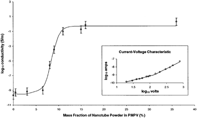 | ||
| Fig. 2 A semilogarithmic plot of the conductivity of the composite for various mass fractions of nanotube powder in PmPV. Inset: Logarithmic current–voltage characteristic for the 8% sample, showing both Ohmic and quadratic regions. Reproduced from ref. 23. Copyright 1998 The American Physical Society. | ||
A composite of a new polymer; poly(p-phenylene vinylene) (PPV), with MWNTs, was investigated by Ago et al.66 They studied the electronic interaction between photoexcited PPV and semiconducting MWNTs. In the ground state, no significant electronic interaction was observed, except for the slight reduction of the π-conjugation of PPV. This was attributed to the introduction of nanoscopic structural disorder of the chains in the composite. In the photoexcited state, PL quenching was observed. Thus, the main electronic interaction was suggested to be energy transfer from photoexcited PPV to the MWNTs.
3.2.1.1. Application of MWNT-conjugated polymer composites as electron-transport layers in OLEDs. Following the various studies on MWNT–PmPV composites and with exciting results, Fournet et al.64 reported an OLED using a MWNT–PmPV composite as the electron-transport layer (ETL) in HTL/M3EH-/ETL device using PVK and poly-TPD-DPX as the HTLs. The use of PVK as HTL and MWNT–PmPV composite with 10% MWNT concentration yielded best results. Also, these triple-layer devices were found to be an order of magnitude brighter than M3EH- single-layer (SL) devices, but with the drawback of an increase in the operating voltage (20–30 V as compared to 8 V for M3EH- SL devices). Thus, the prepared composite was stated to act as a real cathode as well as a hole-blocking material and its use as the ETL in OLEDs to improve the luminescence was proposed. Further studies to understand the role of MWNTs in MWNT–PmPV composites utilized as an ETL in OLED devices were carried out by Fournet et al.65 They fabricated SL, double-layer (DLH and DLE) and triple-layer (TL) devices with the following configurations: ITO/M3EH-/Al (SL), ITO/PVK/M3EH-/Al (DLH), ITO/M3EH-/MWNT–PmPV/Al (DLE), ITO/PVK/M3EH-/MWNT–PmPV/Al (TL). It was found that a potential barrier to both holes as well as electrons was introduced at the M3EH-/MWNT–PmPV composite interface. This barrier decreased with the MWNT-to-polymer mass ratio, leading to larger device currents. A significant increase in efficiency was obtained for the device with an ETL of mass ratio 8%. Above 8% mass ratio, an increased hole leakage into the composite layer was ascribed as the reason for the low efficiency observed. An increase in conductivity, on doping with MWNTs, by over four orders of magnitude in the composite and little quenching of photoluminescence was also observed.
3.2.1.2. Application of MWNT-conjugated polymer composites as hole-injection layers in OLEDs. The use of MWNT composites with PEDOT:PSS, as the hole-injection layer (HIL) in an OLED was first reported by Wang et al.68 They fabricated devices with the configuration PET/ITO/MWNT–PEDOT:PSS composite/Alq3/Al and found that the EL intensity of the OLEDs was significantly increased and the turn-on voltage was decreased by adopting an appropriate concentration of MWNTs in the composite with PEDOT:PSS. It was suggested that MWNT doping improves the hole-injection ability of PEDOT:PSS. Further improvement to the device structure by incorporating a hole-transport layer (HTL) was reported again by Wang et al.69 They fabricated devices with the configuration PET/ITO/MWNT-PEDOT:PSS composite/TPD/Alq3/Al and obtained a maximum luminance of 6800 cd m−2 at a drive voltage of 15 V, which was higher than those obtained from the devices with or without hole-injection layers of PEDOT:PSS.
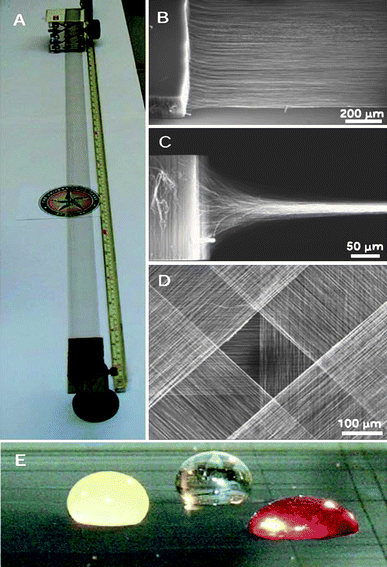 | ||
Fig. 3 (A) A self-supporting 3.4 cm wide, metre-long MWNT sheet that has been hand drawn from a nanotube forest at an average rate of 1 m min−1. (B) SEM image at a 35° angle with respect to the forest plane, capturing a MWNT forest being drawn into a sheet. (C) SEM micrograph showing the cooperative 90° rotation of MWNTs in a forest to form a sheet. (D) SEM micrograph of a two-dimensionally reinforced structure fabricated by overlaying four nanotube sheets with a 45° shift in orientation between successive sheets. (E) Photograph showing two orthogonal as-drawn nanotube sheets supporting droplets of water (∼2.5 mm in diameter), orange juice, and grape juice, where the mass of the droplet is up to 50![[hair space]](https://www.rsc.org/images/entities/char_200a.gif) 000 times that of the contacting nanotube sheets. Reproduced from ref. 67 with permission from AAAS. 000 times that of the contacting nanotube sheets. Reproduced from ref. 67 with permission from AAAS. | ||
3.3. Problems and findings associated with applications of MWNTs in OLEDs
The past few years have witnessed a surge of research efforts in the field of the application of MWNTs to the field of organic electronic devices such as organic light emitting diodes , organic solar cells, organic thin film transistors, etc. In particular, conjugated polymer composites blended with MWNTs have exhibited considerable enhancement in electrical conductivity without any decrease in stability. Moreover, MWNTs have been found to enhance the mechanical strength of the composite as well as act as nanometric heat sinks. Comparing SWNTs and MWNTs, we can say, that from the processing point of view, it is easier to process MWNTs as they are less prone to forming tight bundles. Also, SWNTs generally exist as mixtures of metallic and semiconducting tubes and separating the two types of tubes in a 100% perfect manner is still a puzzle for the scientific community. The presence of both the types of tubes leads to the formation of semiconductive–metallic SWNT Schottky junctions which exhibit high electrical resistance and degrade the performance of the device. Hence, MWNTs, which owing to their larger diameter are generally metallic in nature, offer some significant advantages as compared to SWNTs, for organic electronics applications. Also, we know that, as such, carbon nanotubes are insoluble in most of the organic solvents. They need to be functionalized in order to form solutions, or rather dispersions, with conjugated polymers; a preliminary step in forming composites of carbon nanotubes with conjugated polymers. From this point of view also, MWNTs are more suitable than SWNTs because the functionalization treatment affects only the outer tube in the case of a MWNT and the inner graphene layers remain unaffected, thus preserving the intrinsic electronic structure of the tube. It is important to preserve the electronic structure of the tube when electronic interactions between the tubes and the polymer backbone come into picture and the associated charge-transport properties are important.Some of the problems which are currently overshadowing the field of MWNT-based OLEDs and need to be overcome, in order for this field to emerge over the horizon, are discussed herein. Perhaps, the foremost and the most significant problem associated with MWNTs, in the case of MWNT-conjugated polymer composites, is the protruding of MWNTs from the composite film. It is important to prevent the MWNTs from protruding out from the composite film, in order to avoid direct contact between the nanotube and the metal electrode. Nanotubes protruding from a film can cause a short circuit due to their high conductivity. Hence, the quality of the carbon nanotube-conjugated polymer composite film is crucial for device fabrication. The probability of tubes aligned vertically to the composite film is higher when employing the vacuum filtration technique because the tubes invariably get stuck in the pores of the filter membrane. Hence, this obstacle needs to be paid special attention when fabricating a carbon nanotube-conjugated polymer composite film. Also, the addition of carbon nanotubes to a conjugated polymer, in order to form a composite, in general, leads to a massive increase in surface area of the conjugated polymer, because of the large surface-to-volume ratio of carbon nanotubes and thus, leads to increased electronic interaction between carbon nanotubes and the conjugated polymer backbone, a factor useful with regard to the operation of the associated device. However, the addition of carbon nanotubes also leads to a significant increase in the roughness of the composite film, owing to the intrinsic nature of the carbon nanotubes. The increase in roughness is not beneficial from device point of view as it leads to short circuit problems. In order to decrease the roughness of the composite film, the composite film is coated with a polymer layer (generally PEDOT:PSS). However, too thick a coating of the polymer on top of the composite layer is also harmful as it leads to deterioration of the photocurrent in the device. Hence, a proper balance is necessary between the concentration of carbon nanotubes employed for forming the composite film and the thickness of the polymer coating on top of the composite layer. The greater the concentration of carbon nanotubes in the composite film, the greater the associated roughness of the film and the thicker a subsequent polymer layer is required to be in order to avoid the short circuit problems. Higher concentrations of carbon nanotubes also leads to bundle formation in the composite film because of the attractive force between the carbon nanotubes and the subsequent effective dispersion problems. Moreover, large numbers of bundles formed in the composite film also lead to variation in the thickness of the composite film at various places and hence, inefficient device operation. Since carbon nanotubes cannot be deposited by vacuum evaporation techniques (which lead to more uniform film deposition) and instead depend on spin-coating, inkjet printing, etc., their concentration in the composite film, needs to be optimized properly, before device fabrication, for good results. In order to avoid bundle formation in the film, generally surfactants are employed for dispersing the carbon nanotubes. However, 100% removal of surfactant after film formation so that it does not alter the electronic properties of the film is also a difficult task. Also, because of their intrinsic nature, MWNTs reduce the PL efficiency of the composite because of scattering and absorption. Here again, their concentration needs to be optimized so that the advantages resulting from their incorporation into the composite (such as increase in electrical conductivity) can be harvested rather than cause a deterioration of the beneficial properties of the device. Barriers/challenges like the dispersion of nanotubes in an effective manner in suitable surfactants, the scalability of carbon nanotube film formation methods and their compatibility with large-scale production methods, etc., need to be overcome. Although significant progress has been made in a few systems, the investigations of the carrier transport and performance in the composite-based devices are still quite scarce. A detailed understanding of the interactions between the carbon nanotubes and the local polymer environment are required. Theoretical modelling is required along with experimental investigations to gain insight into the conduction mechanisms at the molecular level. Such efforts will lead to a better understanding of these nanoscale systems and hence, allow tailoring of the device properties according to need. When all this is achieved, only then will the large-scale production of custom-designed devices become possible.
4. Single wall carbon nanotubes (SWNTs)
SWNTs comprise a single graphene cylinder, capped at either end by half a fullerene molecule, and with typical diameters in the range 0.4–3 nm. SWNTs exist as mixtures of metallic and semiconducting tubes and separation of metallic tubes from semiconducting tubes is still one of the active research areas today.70–73 This feature complicates the application of SWNTs in organic electronic devices. Nevertheless, enormous amount of work has been done in the field of applications of SWNTs to organic light emitting diodes , some of which will be elaborated below.4.1. Work function of SWNTs
Various theoretical and experimental studies have established the work function of SWNTs to be ∼4.8–4.9 eV74–76 While Lagemaat et al.74 found the work function of SWNTs to be in the range 4.8–4.9 eV using UPS and XPS, Shiraishi et al.77 found the work function of SWNTs to be 5.05 eV using the photoelectron emission (PEE) method4.2. Applications of SWNTs in OLEDs
SWNTs have been employed in organic light emitting diodes (OLEDs) as hole-injecting electrodes, as charge-transport layers, etc.SWNTs are generally employed either in the form of their composites with conjugated polymers or as plain sheets, in OLEDsStudies to understand the role of SWNTs in a hole-conducting bufferpolymer were carried out by Woo et al.81 They dispersed SWNTs in PEDOT:PSS and formed OLEDs with the configuration: ITO/PEDOT: PSS–SWNT composite/PECCP/LiF/Al. A significant decrease in EL was observed in the devices having the SWNT composite as compared to the devices without the composite. Moreover, the I–V characteristics of the device with the SWNT composite showed I–V2 at low applied voltages (near 2.5 V) whereas the devices without the composite showed I–V5, similar to what was observed in SWNT–PmPV composites.80 The current of the device with the composite abruptly increased at 3 V and then exhibited similar I–V characteristics as that of the device without the composite. The lower power dependence of current in the case of devices having SWNT composite was explained in terms of the hole-trapping nature of SWNTs. It was suggested that the injected holes are initially trapped by SWNTs and the traps generated by SWNTs are filled at around 3 V which leads to an abrupt increase of current and is then followed by a sudden jump to the continuous trap-charge-limit (C-TCL) regime. The significant decrease in EL of the device with the composite was also attributed to hole-traps introduced by SWNTs. Thus, it could be concluded that SWNTs act as hole-trapping centers in SWNT-conjugated polymer composites. However, diametrically contrasting results were reported by Kim et al.82 who synthesized SWNT–PVK composites and utilized them as HTL in OLEDs with the configuration: ITO/PEDOT:PSS/SWNT–PVK composite/DCM-doped Alq3/Li:Al. The devices with SWNTs exhibited better performance in terms of L–V (luminance –voltage) and EQE–I (external quantum efficiency–current) characteristics. Higher luminance and EQE were observed with the increase in mass fraction of SWNTs. It was proposed that facile hole-injection and rigidization of the polymer chains,78 due to polymer–nanotube interactions, come into the picture and this induces more efficient singlet exciton formation at or near to the interface region, leading to higher EL and quantum efficiencies. The EQE was improved by a factor of 2–3 for SWNT concentrations up to 0.2 wt%. A shift in the radiative recombination region of the device (from the EL spectra) was not observed, as observed by Woo et al.79,80 in the case of PmPV–SWNT composites. Kim et al.83 carried out further work, by fabricating hole-only and double-layer-type devices, to understand carrier transport and performance in the SWNT–PVK composite-based devices, with the same configuration as mentioned above. The PL spectra were unaffected by the increasing concentration of SWNTs. Higher luminance together with lower turn-on voltages and higher EQE were observed with an increase in mass fraction of SWNTs. A complete absence of hole-blocking effects in SWNT–PVK composites, as reported by Woo et al.79–81 in PmPV–SWNT composites and PEDOT:PSS-SWNT composites, was observed. It was rather suggested, on the basis of experimental results, that SWNTs act as efficient hole-injectors and transmitters in a poorly conducting PVK matrix. The intercalation of SWNTs in the composite matrix rendered the hole-injection and percolative passage more effective, resulting in the enhanced accumulation of holes at the heterojunction interface. The high density of charge carriers in the recombination region results in higher current density and subsequent higher luminescence. J–V characteristics of the hole-only devices revealed three different regimes: J ∝ V (at low V), J α V2.5±0.5 (at intermediate V) and J ∝ V8.5±1.5 (at high V). The first regime was suggested to correspond to a transition from Ohmic conduction to space-charge-limited (SCL) conduction. The second regime indicated an abrupt transition to the continuous trapped-charge-limited (C-TCL) conduction. Calculation of the effective mobility of the device without SWNTs revealed a value of 1.6 × 10⁻⁷ cm2 V−1 s−1 and the device with SWNTs revealed a value of 7.2 × 10⁻⁷ cm2 V−1 s−1 (at a SWNT concentration of 1.0 wt%). Thus, the increased current density was explained as a result of the co-operative effects of the efficient and facile hole-injection and the percolative transport of holes in the composite system, brought about by the intercalation of SWNTs in the composite.
A new composite: SWNT–MEH- was prepared and utilized in hole-only-type devices and double-layer-type devices by Ha et al.84 For the hole-only devices, the J–V characteristics exhibited three regimes: (i) J ∝ V (at low V) (ii) J ∝ V2 (at intermediate V) and (iii) J ∝ V>3 (at high V). Calculation of effective mobility of the device without SWNTs revealed a value of 2.8 × 10⁻⁷ cm2 V−1 s−1 and the device with SWNTs revealed a value of 1.0 × 10⁻⁶ cm2 V−1 s−1 (at a SWNT concentration of 1.0 wt%). Again, facile hole-injection and percolative interconnections viananotubes in the composite matrix were expected to lead to the formation of highly conductive channels. Devices with the configuration ITO/PEDOT:PSS/MEH-–SWNT composite/DCM-doped Alq3/Li:Al exhibited higher current densities with lower turn-on voltage, with increase in weight fraction of SWNTs. However, the increase in weight fraction of SWNTs did not affect luminance and the EQE decreased at higher SWNT fractions. The lower device efficiency was attributed to the unbalanced densities of electrons and holes induced by the presence of nanotubes in the hole-transporting matrix.
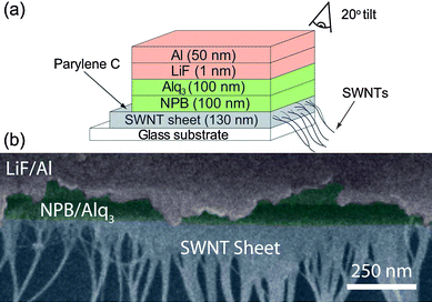 | ||
| Fig. 5 (a) Schematic of the SWNT OLED device and (b) corresponding cross-sectional SEM image at a broken edge taken at a 20° angle from the surface normal. Reproduced from ref. 85 with permission. Copyright 2006 American Institute of Physics. | ||
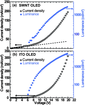 | ||
| Fig. 6 Current density (squares) and luminance (circles) as a function of applied voltage for OLEDs fabricated (a) on carbon nanotube anodes (SWNT OLED) and (b) on oxygen-plasma-treated ITO anodes (ITO OLED). Reproduced from ref. 85 with permission. Copyright 2006 American Institute of Physics. | ||
That SWNTs can compete with ITO as an electrode material was invariably proved. Now, efforts were directed to determine which synthesis technique yielded SWNTs with better properties, with regard to their use as an electrode material. Zhang et al.86 employed two kinds of commercial SWNTs (HiPCO and arc-discharge SWNTs) for fabricating transparent conductive SWNTthin films . They found that arc-discharge SWNTs are overwhelmingly better than HiPCOSWNTs in all of the critical aspects such as surface roughness (7 nm for arc-discharge SWNTs, 11 nm for HiPCOSWNTs), sheet resistance (380 Ω for arc-discharge SWNTs at 87% transparency, 7200 Ω for HiPCOSWNTs at 87% transparency), etc. Thus, it was concluded that arc-discharge SWNTs are more useful for the application of SWNTS as an electrode material. Furthermore, arc-discharge SWNTs were employed in multilayer OLEDs. In order to further improve the properties of arc-discharge SWNTS with regard to their application as an electrode material in OLEDS, some measures were adopted. A PEDOTpassivation layer was applied on top of the SWNT film in order to further reduce the roughness of SWNT film. It was observed that application of a PEDOTpassivation layer on the arc-discharge SWNT film brought down its surface roughness from 7 nm to 3.1 nm (comparable to surface roughness of standard ITO films; determined as 2.4 nm). Secondly, in order to lower the sheet resistance of arc-discharge SWNT films, thionyl chloride doping was adopted. Using the doping technique, optimized films having a sheet resistance of ∼160 Ω/□ at 87% transparency were obtained. These optimized films were used as anodes in OLEDs having the configuration: SWNT film on glass/PEDOT/NPD/Alq3/LiF/Al. A threshold voltage of 5 V and a brightness of 17 cd m−2 at 20 V were obtained. These values of current density and brightness were found to be lower than those of ITO-based OLEDs by 1–2 orders of magnitude. The SWNT devices exhibited high stability and long lifetimes (greater than 4–5 h). Thus, performance comparable to ITO OLEDs was achieved.
A further attempt at improving the roughness of SWNT films was made by Li et al.87 They fabricated polymerlight emitting diodes (PLEDs) with a SWNT anode and PEDOT:PSSbuffer layer and PLEDs with a SWNT anode and a PEDOT:PSS-methanol (1 : 2) mixture as a buffer layer. Using AFM, it was found that the SWNT film exhibited a rms roughness of 6–10 nm, the SWNT film with a PEDOT:PSS overlayer exhibited a rms roughness of 4 nm and the SWNT film with a PEDOT:PSS-methanol overlayer exhibited a rms roughness of 0.96 nm (Fig. 7). Thus, the PEDOT:PSS-methanol overlayer significantly smoothens the SWNT layer.
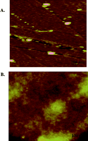 | ||
| Fig. 7 (A) AFM image of SWNT film with a spin-coated PEDOT:PSS overlayer. The rms roughness is 4 nm from the AFM image. (B) AFM image of SWNT film with a spin-coated PEDOT:PSS-methanol (1 : 2) overlayer. The rms roughness is 0.96 nm from the AFM image. Reproduced with permission from ref. 87. Copyright 2006 American Chemical Society. | ||
The effect of this smoothing action was reflected in the device characteristics as well. PLEDs with device configuration SWNT/TFB + TPDSi2/TFB + BT/CsF/Al exhibited a maximum luminance of 10 cd m−2 and a turn-on voltage of 12 V. Whereas PLEDs with device configuration SWNT/PEDOT:PSS-methanol/TFB + TPDSi2/TFB + BT/CsF/Al exhibited a maximum luminance of 1000 cd m−2, maximum current efficiency of ∼0.85 cd A−1 and a turn-on voltage of ∼5 V. A spectacular improvement in device characteristics indeed! Moreover, PLEDs with the device configuration SWNT/PEDOT:PSS-methanol/TFB + TPDSi2/BT/CsF/Al exhibited a maximum luminance of 3500 cd m−2 and a maximum current efficiency of 1.6 cd A−1. The reduction in cathode-induced exciton quenching in case of BT-based devices as compared to TFB + BT-based devices was stated as the reason for the increased luminance and maximum current efficiency in case of BT-based devices. The lifetime of SWNT-based PLEDs was found to be ∼55 h with 1200 cd m−2 initial luminance whereas the lifetime of an ITO-based PLED was found to be ∼52 h with 1400 cd m−2 initial luminance (Fig. 8). Also, the ITO-based PLED exhibited a maximum light output of 20000 cd m−2 and a maximum current efficiency of 6 cd A−1. Although, use of a SWNT anode yielded device characteristics which were slightly inferior in comparison to ITO anode-based PLEDs, the results were still encouraging, keeping in mind the advantages offered by SWNT anodes as compared to ITO anodes.
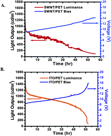 | ||
| Fig. 8 Lifetime characterization of PLEDs having the structures: (A) SWNT on PET/PEDOT-PSS-methanol(30 nm)/TFB + TPDSi2(25 nm)/BT(70 nm)/CsF(1.8 nm)/Al(110 nm) and (B) ITO on PET/PEDOT-PSS-methanol(30 nm)/TFB + TPDSi2(25 nm)/BT(70 nm)/CsF(1.8 nm)/Al(110 nm). Reproduced with permission from ref. 87. Copyright 2006 American Chemical Society. | ||
Once inkjet printing technology of SWNT-polymer composite films gets fully developed, perhaps, more improved devices with carbon nanotubes can be expected to leave the floors of research and university labs and reach the markets. Already, laudable efforts in this direction have been reported.88,89 The films formed with inkjet printing technology can be expected to be more uniform and less rough as compared to films formed by conventional techniques such as spin-coating. One noteworthy point with respect to SWNT films and their utilization in OLEDs, organic photovoltaics (OPVs) etc., is the trade-off which exists between transparency and conductivity of a SWNT film. Enhancement of one of these two parameters generally leads to a degradation of the other. To date, the lowest reported sheet resistance value for a SWNT film is 30 Ω/□ with a transparency of approximately 80%29 which is comparable to ITO (sheet resistance of 10–30 Ω/□ at 85%). However, this value has been reported by one group29 only, and the more commonly reported values range from 120–200 Ω/□ at a transparency around 80–87%.86,87 A simple post-deposition method to improve the conductivity of transparent and conducting SWNTthin films via exposure to nitric acid and thionyl chloride was reported by Parekh et al.90 The functionalized SWNT films exhibited a sheet resistance of ∼30 Ω/□ (comparable to ITO) however with a lower transmittance (∼50%) at 550 nm. At 80 ± 5% transmittance, the functionalized films had resistance values from 150 to 300 Ω/□. However, the SWNT films were found to be extremely flexible as compared to ITO films. It was observed that the electrical resistance of SWNT films remains nearly unchanged after bending while the resistance of ITO films increased by four orders of magnitude. The stability of the films was demonstrated by annealing at temperatures of at least 250 °C in a nitrogen atmosphere and in chloroform. The stability was comparably less in water and methanol. Geng et al.91 exposed SWNT films, formed by the spray method, to nitric acid and obtained a value of the sheet resistance of ∼40 Ω/□ and 70 Ω/□ at 70% and 80% transmittance respectively. An improvement in the conductivity by a factor of ∼4 times was observed. Similar effects were observed in the case of sulphuric acid treatment. It was further observed92 that the enhancement of the optical conductivity by the acid treatment was less prominent than the dc conductivity. Further research on the stability of SWNT films, exposed to nitric acid and thionyl chloride, in air with time and under elevated temperature conditions, was carried out by Jackson et al.93 They obtained a sheet resistance of 105 Ω/□ with a transmittance of 80% for a SWNT film treated with HNO3 and SOCl2. It was observed that the doped films had limited stability in air over time and at elevated temperatures (up to 80 °C). A thin layer of PEDOT:PSS was found to be effective in limiting the degradation of films and even stabilizing the improved sheet resistance of the films. Films capped with PEDOT:PSS demonstrated excellent air stability and thermal stability up to 80 °C.
A new method to further reduce the sheet resistance value was proposed by Valentini et al.44 They applied a magnetic field while casting functionalized SWNT–polymer films on ITO-coated glass and ITO-coated PET substrates. It was found that the sample dewetting under the magnetic field enhances the conductivity of the dried films. For a functionalized SWNT–PEDOT:PSS film on an ITO-coated PET substrate, they obtained a sheet resistance value of 90 Ω/□ at 88% transmittance. A remarkable improvement in lowering of the sheet resistance value. A method based on a spin-coating process for fabricating a transparent SWNT–block copolymer composite film with the sheet resistance tunable from the order of 1014 to 103 Ω/□ was reported by Sung et al.94 However, this method yielded large values of sheet resistance as compared to the other methods. The lowest value for sheet resistance obtained using this method was 6000 Ω/□ with approximately 85% transmittance.
Recently, De et al.95 reported the fabrication of a SWNT–PEDOT:PSS composite film on a PET substrate with a sheet resistance value of 80 Ω/□ and having a transmittance of 75% at 550 nm. They reported a σDC/σOp ratio (ratio of DC conductivity and optical conductivity of the material) of 15 for the composite film, perhaps the highest reported value for σDC/σOp to date.
Geng et al.96,97 fabricated flexible, transparent, conducting films using SWNTs, double-wall carbon nanotubes, thin MWNTs and MWNTs. They found that SWNTs gave the lowest sheet resistance and highest transmittance among the four types of carbon nanotubes and hence, concluded that SWNTs were the best candidates for transparent, conducting films for use as electrodes in OLEDs, OPVs, etc. While using different types of SWNTs it was found that98 the metallicity of SWNTs and the degree of dispersion were the most crucial factors in determining the transparent, conducting film performance. The conductivity of the film is dominated by inter-tube hopping electron transport which is dominated by the degree of dispersion of the nanotubes. So far, efforts have been directed towards lowering of the sheet resistance value. However, the methodologies adopted for fabricating SWNTthin films were limited to lab scale only and were not industrially scalable methods. In this direction, an industrially scalable, fast and simple process for the large-scale fabrication of optically transparent and electrically conducting thin films of SWNTs has recently been reported by Dan et al.99 They employed a rod-coating procedure to coat highly uniform, transparent and conducting SWNTthin films . Films as large as 20 cm × 20 cm have been fabricated on glass surfaces and PET substrates. Furthermore, they have doped the SWNT films with fuming sulphuric acid and this has yielded films with sheet resistance values of 100 and 300 Ω/□ for respective transparencies of 70% and 90% in the visible region. This method of SWNT film coating has been suggested to be more readily adaptable to more controllable and higher throughput methods such as slot-, slide-, and roll-coating. Thus, the method paves the way for the deployment of transparent, conductive SWNT films in large-scale commercial applications. The carbon nanotube transparent and flexible electrode technology is not expected to, but has indeed reached the markets from the floors of research and university labs. Recently Samsung Electronics and Unidym demonstrated the world's first carbon nanotube-based color active matrix electrophoretic display (EPD) e-paper device in a 14.3″ format display (Fig. 9).100 The device utilizes a carbon nanotube transparent electrode. Earlier, Samsung and Unidym had demonstrated the world's first 2.3″ black-and-white active matrix EPD made with carbon nanotubes.100 More exciting and improved innovations are expected to follow.
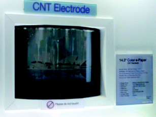 | ||
| Fig. 9 World's first carbon nanotube-based color active matrix electrophoretic display (EPD) e-paper device in a 14.3″ format display, demonstrated by Samsung (http://www.unidym.com/press/pr_081016.html). | ||
4.3. Problems and findings associated with applications of SWNTs in OLEDs
Over the past few years, the research efforts of the scientific community have been more favored towards SWNTs as is evident from the number of research papers published using SWNTs in organic electronics applications as compared to the number of research papers published using MWNTs in organic electronics applications. SWNTs have typical diameters in the range 0.4–3 nm whereas MWNTs can be synthesized with typical diameters as large as 100 nm. For OPV and OLED applications, the thickness of the organic layer is typically <200 nm. One distinct advantage in the case of SWNTs as compared to MWNTs is that since SWNTs have small diameters, even if the tubes get bundled in a manner where one tube lies on top of another and so on, the effective diameter of the complete bundle rarely exceeds 20 nm and hence, the probability of device failure because of increased organic layer thickness is less. Since bundle formation is a necessary part of working with carbon nanotubes (because of attractive forces which exists between carbon nanotubes) and the way in which these bundles are formed, cannot be controlled; hence, SWNTs are somewhat better than MWNTs. One significant processing bottleneck which exists in the case of SWNTs is the existence of both metallic and semiconducting nanotubes within a sample. Assuming equal probability of all chiral vectors, two-thirds of SWNTs are semiconducting and the remaining one third are metallic. Several techniques have been developed to separate semiconducting from metallic nanotubes, however, 100% separation of the two types of tubes is still a mystery. The other problems which have been mentioned in the case of MWNTs such as protruding of tubes from the composite film, increase in surface roughness of the film, bundle formation in the film, removal of surfactant from the film where surfactants are employed, etc. exist in the case of SWNTs as well. We will be throwing some light here on other critical factors (problems as well as advantages) which are specific to SWNTs.One prime area in the field of OLEDs using SWNTs, which is rapidly emerging, is the application of SWNT sheets as electrodes in OLEDs. The relatively short supply of indium and the associated disadvantages of ITO, as mentioned earlier in this article, are responsible for the sudden boost which this field has received in recent years. Regarding the application of SWNT sheets as electrodes in OLEDs, there are certain factors which deserve prime attention while utilizing SWNTs for such a purpose. These factors include the sheet resistance of the film, the surface roughness of the film, the transparency requirements of the film, the ratio of DC conductivity and optical conductivity of the composite film (σDC/σOp ratio), etc. As in the case of MWNTs, here also, a trade-off exists between the various parameters and we need to carefully optimize the values of the various parameters before designing a SWNT film as an electrode in OLED applications. A value of σDC/σOp ≥35 (in order to achieve a sheet resistance ≤100 Ω/□ and an optical transparency ≥ 90% at 550 nm)95 is required in order to meet minimum industry standards for a flexible, transparent and conductive electrode material in devices such as OLEDs, solar cells, etc. Clearly, SWNTs appear as the closest contenders in this race. The transmittance at 550 nm vs. the sheet resistance is commonly used to compare the opto-electronic properties of SWNTthin films . It has been observed that enhancement of transmittance at 550 nm leads to enhancement in sheet resistance as well, an undesirable result. Hence, generally attempts are made to reach a trade-off point where both these parameters can be optimized, giving desirable results for device operation. Regarding the surface roughness of the film, it is always desirable to have as low a value of surface roughness as possible in order to avoid short circuits in device operation. The methods to lower the surface roughness include using arc-discharge SWNTs as compared to SWNTs produced by other methods,86 designing films having SWNT concentration near to or slightly greater than the percolation threshold value in the case of SWNT-conjugated polymer composites and covering the SWNT layer with a polymer layer (say PEDOT:PSS or a PEDOT:PSS-methanol (1 : 2) mixture) in the case of SWNT sheets. In case of composites, at the percolation threshold value, conductive pathways are established throughout the film and hence, the purpose of addition of SWNTs is fulfilled. Adding SWNTs much more than the percolation threshold concentration alters the intrinsic properties of the composite system as well as increasing the surface roughness value of the composite film. Hence, in the case of SWNT-conjugated polymer composites it is always beneficial to go for SWNT concentrations either equal to or slightly greater than the percolation threshold value. In the case of plain SWNT sheets, the surface roughness values can be many times higher and the measures to reduce the surface roughness include coating the SWNT layer with a polymer layer (not too thick as a thicker polymer film will deteriorate the photocurrent in the device) such as PEDOT:PSS or a PEDOT:PSS-methanol (1 : 2) mixture as a buffer layer.87 Also, films capped with PEDOT:PSS have demonstrated excellent air stability and thermal stability up to 80 °C.93 In order to reduce the sheet resistance of the SWNT film, various chemical treatments can be adopted, such as doping with thionyl chloride,86 exposure to nitric acid and thionyl chloride,90etc. In other words, we can say that desirable tuning of the SWNT film properties, with regard to their application as electrode materials in OLEDs, OPVs, etc., can be done via different chemical strategies. This is not possible in case of ITO—the conventional favorite electrode material. Also, SWNT films are far more flexible than ITO, hence useful in organic electronics applications where flexibility is an important characteristic.
5. Conclusion and perspectives
Currently, two different schools of thought exist regarding the suitability of MWNTs and SWNTs, in the form of nanocomposites with conducting polymers and as plain sheets, for their application in OLEDs, organic solar cells, etc. Various research groups have produced different results and it would be perhaps, not wrong to say that both MWNTs as well as SWNTs have exhibited commendable performance in organic electronics applications. Carbon nanotubes (MWNTs as well as SWNTs) have been found to act as hole-blocking materials in a few systems and as efficient hole-injectors in some systems, while for some systems, energy transfer was primarily observed in the composite region and no hole- or electron-transfer was observed. It cannot be generalized that carbon nanotubes are efficient hole-injectors or efficient hole-blocking materials with regard to their application as transport layers (in the form of composites with conjugated polymers) in OLEDs. The characteristics exhibited have been observed to be different in different polymer systems. This observation brings to light the fact that the nature of the polymer and the nature of the polymer–carbon nanotube interactions (particularly electronic interactions) is important in a conjugated polymer–carbon nanotube composite system. Hence, before using any carbon nanotube-conjugated polymer composite system as a transport layer in OLEDs, a detailed study of the nature and extent of interactions (electronic, structural, etc.) between carbon nanotubes and the conjugated polymer should be carried out. Based on the results of such a study, carbon nanotubes (MWNTs or SWNTs) should be applied as an electron-transport layer or as a hole-transport layer in an OLED. Perhaps, the most excellent results regarding the application of carbon nanotubes in OLEDs have been obtained when they have been used as transparent electrodes in OLEDs, for as transparent electrodes, they have provided some distinct advantages over the conventional ITO. The large surface area offered by carbon nanotube films, combined with the three-dimensional nature of hole-injection, mechanical flexibility of the carbon nanotube film, good acid resistance, room temperature processing which makes both top and bottom emission devices possible, etc. overshadow the better device characteristics offered by ITO anode-based OLEDs. Moreover, since indium is in relatively short supply whereas carbon is the most abundant element in nature, the future appears to be brighter for carbon nanotube-based OLEDs!Acknowledgements
One of the authors (M. B.) acknowledges the fellowship support (Teaching-cum-Research Fellowship) from Netaji Subhas Institute of Technology, New Delhi, India.References
- S. Iijima, Helical microtubules of graphitic carbon, Nature, 1991, 354, 56–58 CrossRef CAS.
- Chin Spencer, Flex display market to grow 83.5% a year, EE Times Online, 2006 Search PubMed.
- S. Reich, C. Thomsen and J. Maultzsch, Carbon Nanotubes, Wiley-VCH, Weinheim, 2004 Search PubMed.
- S. J. Tans, M. H. Devorat, H. Dai, A. Thess, R. E. Smalley, L. J. Geerligs and C. Dekker, Individual single-wall carbon nanotubes as quantum wires, Nature, 1997, 386, 474–477 CrossRef CAS.
- B. I. Yakobson and P. Avouris, Mechanical properties of carbon nanotubes, in Carbon Nanotubes, Springer Verlag, Berlin, 2001,vol. 80, pp. 287–327 Search PubMed.
- P. Serp, M. Corrias and P. Kalck, Carbon nanotubes and nanofibers in catalysis, Appl. Catal., A, 2003, 253, 337–358 CrossRef CAS.
- W. J. Liang, M. Bockrath, D. Bozovic, J. H. Hafner, M. Tinkham and H. Park, Fabry-perot interference in a nanotube electron waveguide, Nature, 2001, 411, 665–669 CrossRef CAS.
- A. Maeda, S. Matsumoto, H. Kishida, T. Takenobu, Y. Iwasa, M. Shiraishi, M. Ata and H. Okamoto, Large optical nonlinearity of semiconducting single-walled carbon nanotubes under resonant excitations, Phys. Rev. Lett., 2005, 94, 047404 CrossRef CAS.
- S. Tatsuura, M. Furuki, Y. Sato, I. Iwasa, M. Tian and H. Mitsu, Semiconductor carbon nanotubes as ultrafast switching materials for optical telecommunications, Adv. Mater., 2003, 15, 534–537 CrossRef CAS.
- R. H. Baughman, A. A. Zakhidov and W. A. deHeer, Carbon nanotubes—the route towards applications, Science, 2002, 297, 787–792 CrossRef CAS.
- P. L. McEuen, Single-wall carbon nanotubes, Physics World, 2000, 13, 31–36 Search PubMed.
- A. J. Miller, R. A. Hatton and S. R. P. Silva, Interpenetrating mutiwall carbon nanotube electrodes for organic solar cells, Appl. Phys. Lett., 2006, 89, 133117 CrossRef.
- R. A. Hatton, A. J. Miller and S. R. P. Silva, Carbon Nanotubes: a multi-functional material for organic optoelectronics, J. Mater. Chem., 2008, 18, 1183–1192 RSC.
- D. M. Guldi, G. M. A. Rahman, F. Zerbetto and M. Prato, Carbon nanotubes in electron donor-acceptor nanocomposites, Acc. Chem. Res., 2005, 38, 871–878 CrossRef CAS.
- H. Ago, Th. Kugler, F. Cacialli, K. Petritsch, R. H. Friend, W. R. Salaneck, Y. Ono, T. Yamabe and K. Tanaka, Workfunction of purified and oxidized carbon Nanotubes, Synth. Met., 1999, 103, 2494–2495 CrossRef CAS.
- H. Ago, Th. Kugler, F. Cacialli, W. R. Salaneck, S. P. Shaffer Milo, A. H. Windle and R. H. Friend, Work functions and functional groups of multiwall carbon nanotubes, J. Phys. Chem. B, 1999, 103, 8116–8121 CrossRef CAS.
- S. Kirkpatrick, Percolation and conduction, Rev. Mod. Phys., 1973, 45, 574–588 CrossRef.
- R. Zallen, The physics of amorphous solidsWiley, New York, 1983 Search PubMed.
- D. Stauffer and A. Aharony, Introduction to percolation theoryTaylor & Francis, London, 1994 Search PubMed.
- G. E. Pike and C. H. Seager, Percolation and conductivity: a computer study I, Phys. Rev. B: Condens. Matter Mater. Phys., 1974, 10, 1421–1434 CrossRef.
- B. E. Kilbride, J. N. Coleman, J. Fraysse, P. Fournet, M. Cadek, A. Drury, H. Hutzler, S. Roth and W. J. Blau, Experimental observation of scaling laws for alternating current and direct current conductivity in polymer–carbon nanotube composite thin films, J. Appl. Phys., 2002, 92, 4024–4030 CrossRef CAS.
- S. H. Munson-McGee, Estimation of the critical concentration in an anisotropic percolation network, Phys. Rev. B: Condens. Matter Mater. Phys., 1991, 43, 3331–3336 CrossRef.
- J. N. Coleman, S. Curran, A. B. Dalton, A. P. Davey, B. McCarthy, W. Blau and R. C. Barklie, Percolation-dominated conductivity in a conjugated-polymer–carbon-nanotube composite, Phys. Rev. B: Condens. Matter Mater. Phys., 1998, 58, R7492–R7495 CrossRef CAS.
- T. V. Sreekumar, T. Liu, S. Kumar, L. M. Ericson, R. H. Hauge and R. E. Smalley, Single wall carbon nanotube films, Chem. Mater., 2003, 15, 175–178 CrossRef CAS.
- J. E. Trancik, S. C. Barton and J. Hone, Transparent and catalytic carbon nanotube films, Nano Lett., 2008, 8, 982–987 CrossRef CAS.
- N. P. Armitage, J.-C. P. Gabriel and G. Gruner, Quasi-Langmuir–Blodgett thin film deposition of carbon nanotubes, J. Appl. Phys., 2004, 95, 3228–3230 CrossRef CAS.
- Y. Kim, N. Minami, W. Zhu, S. Kazaoui, R. Azumi and M. Matsumoto, Langmuir–Blodgett Films of Single-Wall Carbon Nanotubes: Layer-by-layer deposition and in-plane orientation of tubes, Jpn. J. Appl. Phys., 2003, 42, 7629–7634 CrossRef CAS.
- M. E. Spotnitz, D. Ryan and H. A. Stone, Dip coating for the alignment of carbon nanotubes on curved surfaces, J. Mater. Chem., 2004, 14, 1299–1302 RSC.
- Z. Wu, Z. Chen, X. Du, J. M. Logan, J. Sippel, M. Nikolou, K. Kamaras, J. R. Reynolds, D. B. Tanner, A. F. Hebard and A. G. Rinzler, Transparent, conductive carbon nanotube films, Science, 2004, 305, 1273–1276 CrossRef CAS.
- E. Kymakis, G. Klapsis, E. Koudoumas, E. Stratakis, N. Kornilios, N. Vidakis and Y. Franghiadakis, Carbon nanotube/PEDOT: PSS electrodes for organic photovoltaics, Eur. Phys. J.: Appl. Phys., 2006, 36, 257–259 CrossRef CAS.
- M. Zhang, Y. Yan, K. Gong, L. Mao, Z. Guo and Y. Chen, Electrostatic layer-by-layer assembled carbon nanotube multilayer film and its electrocatalytic activity for O2 reduction, Langmuir, 2004, 20, 8781–8785 CrossRef CAS.
- J. S. Moon, J. H. Park, T. Y. Lee, Y. W. Kim, J. B. Yoo, C. Y. Park, J. M. Kim and K. W. Jin, Transparent conductive film based on carbon nanotubes and PEDOT composites, Diamond Relat. Mater., 2005, 14, 1882–1887 CrossRef CAS.
- L. J. Lanticse, Y. Tanabe, K. Matsui, Y. Kaburagi, K. Suda, M. Hoteida, M. Endo and E. Yasuda, Shear-induced preferential alignment of carbon nanotubes resulted in anisotropic electrical conductivity of polymer composites, Carbon, 2006, 44, 3078–3086 CrossRef CAS.
- S. K. Kim and H. Lee, Fabrication of patterned single-walled carbon nanotube films using electrophoretic deposition, Ultramicroscopy, 2008, 108, 1005–1008 CrossRef CAS.
- S. Shin, Y. K. Baek, Y. K. Choi and H. T. Jung, Self-Assembled Carbon Nanotube Network Films Field Effect Transistor for Biosensor Application, IEICE Tech. Rep., 2008, 108, 135–137 Search PubMed , no.122 SDM2008-84.
- Y. I. Song, C. M. Yang, D. Y. Kim, H. Kanoh and K. Kaneko, Flexible transparent conducting single-wall carbon nanotube film with network bridging method, J. Colloid Interface Sci., 2008, 318, 365–371 CrossRef CAS.
- A. Ansaldo, V. Skakalova, E. D. Zitti, D. Ricci and S. Roth, Catalytic chemical vapour deposition growth of single wall carbon nanotube films on different substrates for transparent electronic devices, Phys. Status Solidi B, 2007, 244, 3935–3938 CrossRef CAS.
- K. Kordás, T. Mustonen, G. Tóth, H. Jantunen, M. Lajunen, C. Soldano, S. Talapatra, S. Kar, R. Vajtai and P. M. Ajayan, Inkjet printing of electrically conductive patterns of carbon nanotubes, Small, 2006, 2, 1021–1025 CrossRef CAS.
- L. Hu, G. Gruner, D. Li, R. B. Kaner and J. Cech, Patternable transparent carbon nanotube films for electrochromic devices, J. Appl. Phys., 2007, 101, 016102 CrossRef.
- Y. Zhou, L. Hu and G. Grüner, A method of printing carbon nanotube thin films, Appl. Phys. Lett., 2006, 88, 123109 CrossRef.
- N. Saran, K. Parikh, D. S. Suh, E. Munoz, H. Kolla and S. K. Manohar, Fabrication and characterization of thin films of single-walled carbon nanotube bundles on flexible plastic substrates, J. Am. Chem. Soc., 2004, 126, 4462–4463 CrossRef CAS.
- J. H. Shin, D. W. Shin, S. P. Patole, J. H. Lee, S. M. Park and J. B. Yoo, Smooth, transparent, conducting and flexible SWCNT films by filtration-wet transfer processes, J. Phys. D: Appl. Phys., 2009, 42, 045305 CrossRef.
- M. A. Meitl, Y. Zhou, A. Gaur, S. Jeon, M. L. Usrey, M. S. Strano and J. A. Rogers, Solution casting and transfer printing single-walled carbon nanotube films, Nano Lett., 2004, 4, 1643–1647 CrossRef CAS.
- L. Valentini, M. Cardinali, D. Bagnis and J. M. Kenny, Solution casting of transparent and conductive carbon nanotubes/poly(3,4-ethylenedioxythiophene)-poly(styrenesulfonate) films under a magnetic field, Carbon, 2008, 46, 1513–1517 CrossRef CAS.
- X. Yu, R. Rajamani, K. A. Stelson and T. Cui, Carbon nanotube based transparent conductive thin films, J. Nanosci. Nanotechnol., 2006, 6, 1939–1944 CrossRef CAS.
- X. Yu, R. Rajamani, K. A. Stelson and T. Cui, Fabrication of carbon nanotube based transparent conductive thin films using layer-by-layer technology, Surf. Coat. Technol., 2008, 202, 2002–2007 CrossRef CAS.
- L. A. Rowley, G. C. Irvin, C. C. Anderson and D. Majumdar U. S. Patent Appl. No. 20060188723, 2006.
- H. L. Hartnagel, A. L. Dawar, A. K. Jain and C. Jagadish, Semiconducting ttransparent thin films, IOP Publishing, Bristol, UK, 1995 Search PubMed.
- D. S. Ginley and C. Bright, Special Issue on Transparent Conducting Oxides, MRS Bull., 2000, 25.
- M. Chhowalla, Transparent and conducting SWNT thin films for flexible electronics, Journal of the SID, 2007, 15/12, 1085–1088 Search PubMed.
- D. R. Cairns, R. P. Witte II, D. K. Sparacin, S. M. Sachsman, D. C. Paine, G P and R. R. Newton, Strain-dependent electrical resistance of tin-doped indium oxide on polymer substrates, Appl. Phys. Lett., 2000, 76, 1425–1427 CrossRef CAS.
- G. Gruner, Carbon nanonets spark new electronics, Sci. Am., 2007, 296, 76–83 CAS.
- A. R. Schlatmann, D. W. Floet, A. Hillberer, F. Garten, P. J. M. Smulders, T. M. Klapwijk and G. Hadziioannou, Indium contamination from the indium–tin–oxide electrode in polymer light-emitting diodes, Appl. Phys. Lett., 1996, 69, 1764–1766 CrossRef CAS.
- J. C. Scott, J. H. Kaufman, P. J. Brock, R. DiPietro, J. Salem and J. A. Goitia, Degradation and failure of MEH_PPV light emitting diodes, J. Appl. Phys., 1996, 79, 2745–2751 CrossRef CAS.
- L. Chkoda, C. Heske, M. Sokolowski, E. Umbach, F. Steuber, J. Staudigel, M. Stößel and J. Simmerer, Work function of ITO substrates and band-offsets at the TPD/ITO interface determined by photoelectron spectroscopy, Synth. Met., 2000, 111–112, 315–319 CrossRef CAS.
- Y. Park, V. Choong, Y. Gao, B. R. Hsieh and C. W. Tang, Work function of indium tin oxide transparent conductor measured by photoelectron spectroscopy, Appl. Phys. Lett., 1996, 68, 2699–2701 CrossRef CAS.
- D. J. Milliron, I. G. Hill, C. Shen, A. Kahn and J. Schwartz, Surface oxidation activates indium tin oxide for hole injection, J. Appl. Phys., 2000, 87, 572–576 CrossRef CAS.
- J. M. Phillips, J. Kwo, G. A. Thomas, S. A. Carter, R. J. Cava, S. Y. Hou, J. J. Krajewski, J. H. Marshall, W. F. Peck, D. H. Rapkine and R. B. V. Dover, Transparent conducting thin films of GaInO3, Appl. Phys. Lett., 65, 115–117 Search PubMed.
- J. Ni, H. Yan, A. Wang, Y. Yang, C. L. Stern, A. W. Metz, S. Jin, L. Wang, T. J. Marks, J. R. Ireland and C. R. Kannewurf, MOCVD-derived highly transparent, conductive zinc- and tin-doped indium oxide thin films: precursor synthesis, metastable phase film growth and characterization, and application as anodes in polymer light-emitting diodes, J. Am. Chem. Soc., 2005, 127, 5613–5624 CrossRef CAS.
- S. Han, X. Feng, Z. H. Lu, D. Johnson and R. Wood, Transparent-cathode for top-emission organic light-emitting diodes, Appl. Phys. Lett., 2003, 82, 2715–2717 CrossRef CAS.
- D. B. Romero, M. Carrard, W. D. Heer and L. Zuppiroli, A carbon nanotube/organic semiconducting polymer heterojunction, Adv. Mater., 1996, 8, 899–902 CAS.
- S. A. Curran, P. M. Ajayan, W. J. Blau, D. L. Carroll, J. N. Coleman, A. B. Dalton, A. P. Davey, A. Drury, B. McCarthy, S. Maier and A. Strevens, A composite from poly(m-phenylenevinylene-co-2,5-dioctoxy-p-phenylenevinylene) and carbon nanotubes: a novel material for molecular optoelectronics, Adv. Mater., 1998, 10, 1091–1093 CrossRef CAS.
- A. B. Dalton, H. J. Byrne, J. N. Coleman, S. Curran, A. P. Davey, B. McCarthy and W. Blau, Optical absorption and fluorescence of a multiwalled-nanotube–polymer composite, Synth. Met., 1999, 102, 1176–1177 CrossRef CAS.
- P. Fournet, D. F. O. Brien, J. N. Coleman, H. H. Horhold and W. J. Blau, A carbon nanotube composite as an electron transport layer for M3EH-PPV based light-emitting diodes, Synth. Met., 2001, 121, 1683–1684 CrossRef CAS.
- P. Fournet, J. N. Coleman, B. Lahr, A. Drury, W. J. Blau, D. F. O. Brien and H. H. Horhold, Enhanced brightness in organic light-emitting diodes using a carbon nanotube composite as an electron-transport layer, J. Appl. Phys., 2001, 90, 969–975 CrossRef CAS.
- H. Ago, M. S. P. Shaffer, D. S. Ginger, A. H. Windle and R. H. Friend, Electronic interaction between photoexcited poly(p-phenylene vinylene) and carbon nanotubes, Phys. Rev. B: Condens. Matter Mater. Phys., 2000, 61, 2286–2290 CrossRef CAS.
- M. Zhang, S. Fang, A. A. Zakhidov, S. B. Lee, A. E. Aliev, C. D. Williams, K. R. Atkinson and R. H. Baughman, Strong, transparent, multifunctional, carbon nanotube sheets, Science, 2005, 309, 1215–1219 CrossRef CAS.
- G. F. Wang, X. M. Tao, W. Chen, R. X. Wang and A. Yang, Improvement in performance of organic light emitting devices by inclusion of multi-wall carbon nanotubes, J. Lumin., 2007, 126, 602–606 CrossRef CAS.
- G. F. Wang, X. M. Tao and R. X. Wang, Fabrication and characterization of OLEDs using PEDOT:PSS and MWCNT nanocomposites, Compos. Sci. Technol., 2008, 68, 2837–2841 CrossRef CAS.
- R. Krupke, F. Hennrich, H. V. Löhneysen and M. M. Kappes, Separation of metallic from semiconducting single-walled carbon nanotubes, Science, 2003, 301, 344–347 CrossRef CAS.
- Y. Maeda, S. I. Kimura, M. Kanda, Y. Hirashima, T. Hasegawa, T. Wakahara, Y. Lian, T. Nakahodo, T. Tsuchiya, T. Akasaka, J. Lu, X. Zhang, Z. Gao, Y. Yu, S. Nagase, S. Kazaoui, N. Minami, T. Shimizu, H. Tokumoto and R. Saito, Large scale separation of metallic and semiconducting single-walled carbon nanotubes, J. Am. Chem. Soc., 2005, 127, 10287–10290 CrossRef CAS.
- S. Campidelli, M. Meneghetti and M. Prato, Separation of metallic and semiconducting s single-walled carbon nanotubes via covalent functionalization, Small, 2007, 3, 1672–1676 CrossRef CAS.
- T. Lutz and K. J. Donovan, Macroscopic scale separation of metallic and semiconducting nanotubes by dielectrophoresis, Carbon, 2005, 43, 2508–2513 CrossRef CAS.
- J. van de Lagemaat, T. M. Barnes, G. Rumbles, S. E. Shaheen, T. J. Coutts, C. Weeks, I. Levitsky, J. Peltola and P. Glatkowski, Organic solar cells with carbon nanotubes replacing In2O3:Sn as the transparent electrode, Appl. Phys. Lett., 2006, 88, 233503 CrossRef.
- J. Zhao, J. Han and J. P. Lu, Work functions of pristine and alkali-metal intercalated carbon nanotubes and bundles, Phys. Rev. B: Condens. Matter Mater. Phys., 2002, 65, 193401 CrossRef.
- S. Suzuki, C. Bower, Y. Watanabe and O. Zhou, Work functions and valence band states of pristine and Cs-intercalated single-walled carbon nanotube bundles, Appl. Phys. Lett., 2000, 76, 4007–4009 CrossRef CAS.
- M. Shiraishi and M. Ata, Work function of carbon nanotubes, Carbon, 2001, 39, 1913–1917 CrossRef CAS.
- S. Curran, A. P. Davey, J. Coleman, A. Dalton, B. M. Carthy, S. Maier, A. Drury, D. Gray, M. Brennan, K. Ryder, M. Chapelle, C. Journet, P. Bernier, H. J. Byrne, D. Carroll, P. M. Ajayan, S. Lefrant and W. Blau, Evolution and evaluation of the polymer/nanotube composite, Synth. Met., 1999, 103, 2559–2562 CrossRef CAS.
- H. S. Woo, R. Czerw, S. Webster, D. L. Carroll, J. Ballato, A. E. Strevens, D. O. Brien and W. J. Blau, Hole blocking in carbon nanotube-polymer composite organic light emitting diodes based on poly(m-phenylene vinylene-co-2,5-dioctoxy-p-phenylene vinylene), Appl. Phys. Lett., 2000, 77, 1393–1395 CrossRef CAS.
- H. S. Woo, Y. B. Kim, R. Czerw, D. L. Carroll, J. Ballato and P. M. Ajayan, Tailoring hole transport in organic light emitting devices using carbon nanotube–polymer nanocomposites, J. Korean Phys. Soc., 2004, 45, 507–511 Search PubMed.
- H. S. Woo, R. Czerw, S. Webster, D. L. Carroll, J. W. Park and J. H. Lee, Organic light emitting diodes fabricated with single wall carbon nanotubes dispersed in a hole conducting buffer: the role of carbon nanotubes in a hole conducting polymer, Synth. Met., 2001, 116, 369–372 CrossRef.
- J. Y. Kim, M. Kim, H. M. Kim, J. Joo and J. H. Choi, Electrical and optical studies of organic light emitting devices using SWCNTs-polymer nanocomposites, Opt. Mater., 2003, 21, 147–151 CrossRef CAS.
- J. Y. Kim, M. Kim and J. H. Choi, Characterization of light emitting devices based on a single-walled carbon nanotube–polymer composite, Synth. Met., 2003, 139, 565–568 CrossRef CAS.
- Y. G. Ha, E. A. You, B. J. Kim and J. H. Choi, Fabrication and characterization of OLEDs using MEH-PPV and SWCNT nanocomposites, Synth. Met., 2005, 153, 205–208 CrossRef CAS.
- C. M. Aguirre, S. Auvray, S. Pigeon, R. Izquierdo, P. Desjardins and R. Martel, Carbon nanotube sheets as electrodes in organic light-emitting diodes, Appl. Phys. Lett., 2006, 88, 183104 CrossRef.
- D. Zhang, K. Ryu, X. Liu, E. Polikarpov, J. Ly, M. E. Tompson and C. Zhou, Transparent, conductive, and flexible carbon nanotube films and their application in organic light-emitting diodes, Nano Lett., 2006, 6, 1880–1886 CrossRef CAS.
- J. Li, L. Hu, L. Wang, Y. Zhou, G. Gruner and T. J. Marks, Organic light-emitting diodes having carbon nanotube anodes, Nano Lett., 2006, 6, 2472–2477 CrossRef CAS.
- W. R. Small and M. Panhuis, Inkjet printing of transparent, electrically conducting single-walled carbon-nanotube composites, Small, 2007, 3, 1500–1503 CrossRef.
- T. Mustonen, K. Kordas, S. Saukko, G. Toth, J. S. Penttila, P. Helisto, H. Seppa and H. Jantunen, Inkjet printing of transparent and conductive patterns of single-walled carbon nanotubes and PEDOT–PSS composites, Phys. Status Solidi B, 2007, 244, 4336–4340 CrossRef CAS.
- B. B. Parekh, G. Fanchini, G. Eda and M. Chhowalla, Improved conductivity of transparent single-wall carbon nanotube thin films via stable postdeposition functionalization, Appl. Phys. Lett., 2007, 90, 121913 CrossRef.
- H. Z. Geng, K. K. Kim, K. P. So, Y. S. Lee, Y. Chang and Y. H. Lee, Effect of acid treatment on carbon-nanotube based flexible transparent conducting films, J. Am. Chem. Soc., 2007, 129, 7758–5779 CrossRef CAS.
- H. Z. Geng, D. S. Lee, K. K. Kim, G. H. Han, H. Park and Y. H. Lee, Absorption spectroscopy of surfactant-dispersed carbon nanotube film: modulation of electronic structures, Chem. Phys. Lett., 2008, 455, 275–278 CrossRef CAS.
- R. Jackson, B. Domercq, R. Jain, B. Kippelen and S. Graham, Stability of doped transparent carbon nanotube electrodes, Adv. Funct. Mater., 2008, 18, 2548–2554 CrossRef CAS.
- J. Sung, P. S. Jo, H. Shin, J. Huh, B. G. Min, D. H. Kim and C. Park, Transparent, low-electric-resistance nanocomposites of self-assembled block copolymers and SWNTs, Adv. Mater., 2008, 20, 1505–1510 CrossRef CAS.
- S. De, P. E. Lyons, S. Sorel, E. M. Doherty, P. J. King, W. J. Blau, P. N. Nirmalraj, J. J. Boland, V. Scardaci, J. Joimel and J. N. Coleman, Transparent, flexible, and highly conductive thin films based on polymer-nanotube composites, ACS Nano, 2009, 3, 714–720 CrossRef CAS.
- H. Z. Geng, D. S. Lee, K. K. Kim, S. J. Kim, J. J. Bae and Y. H. Lee, Effect of carbon nanotube type in fabricating flexible transparent conducting films, J. Korean Phys. Soc., 2008, 53, 979–985 Search PubMed.
- H. Z. Geng and Y. H. Lee, Transparent conducting films by using carbon nanotubes, in Nanoscale Phenomena—Basic Science to Device Applications, Springer, New York, 2007, pp. 15–28 Search PubMed.
- H. Z. Geng, K. K. Kim, K. Lee, G. Y. Kim, H. K. Choi, D. S. Lee, K. H. An and Y. H. Lee, Dependence of material quality on performance of flexible transparent conducting films with single-walled carbon nanotubes, Nano: Brief Reports and Reviews, 2007, 2, 157–167 Search PubMed.
- B. Dan, G. C. Irvin and M. Pasquali, Continuous and scalable fabrication of transparent conducting carbon nanotube films, ACS Nano, 2009, 3, 835–843 CrossRef CAS.
- http://www.unidym.com/press/pr_081016.html .
| This journal is © The Royal Society of Chemistry 2009 |