DOI:
10.1039/B9NR00104B
(Minireview)
Nanoscale, 2009,
1, 96-105
Selective generation of single-walled carbon nanotubes with metallic, semiconducting and other unique electronic properties
Received
8th June 2009
, Accepted 11th August 2009
First published on 28th August 2009
Abstract
As-synthesized single-walled carbon nanotubes (SWNTs) are mixtures of semiconducting and metallic species and separation of the two is of crucial importance for many applications. In this article, the methods employed for the enrichment of semiconducting and metallic SWNTs are presented, along with possible procedures to prepare either of the species selectively. Equally important are the methods for chirality selection. The discovery of metal-semiconductor transitions in SWNTs induced by interaction with electron donor and acceptor molecules is not only of academic interest, but may also find applications. Synthesis of Y-junction SWNTs with unique electronic properties at the junction is yet to be fully accomplished.
 C. N. R. Rao C. N. R. Rao | C. N. R. Rao obtained his PhD degree from Purdue University (1958) and DSc degree from the University of Mysore (1961). He is the National Research and Linus Pauling Research Professor at the Jawaharlal Nehru Centre for Advanced Scientific Research and Honorary Professor at the Indian Institute of Science (both at Bangalore). His research interests are mainly in the chemistry of materials. He has authored nearly 1200 research papers and edited or written 30 books in materials chemistry. He is the recipient medals from UNESCO, the Royal Society, and the International Union of Materials Research Societies. |
 Rakesh Voggu Rakesh Voggu | Rakesh Voggu received his MSc (Chemistry) degree from University of Hyderabad in 2005. He is working towards his PhD degree under Prof. C. N. R. Rao at the Jawaharlal Nehru Centre for Advanced Scientific Research. His work pertains to various aspects of nanocrystals and carbon nanostructures. |
 A. Govindaraj A. Govindaraj | A. Govindaraj obtained his PhD degree from the University of Mysore and is a Senior Scientific Officer at the Indian Institute of Science, and Honorary Faculty Fellow at the Jawaharlal Nehru Centre for Advanced Scientific Research. He works on different types of nanomaterials. He has authored more than 100 research papers and co-authored a book on nanotubes and nanowires. |
Introduction
Since the discovery of carbon nanotubes,1 several methods have been reported for the synthesis of multi-walled, double-walled and single-walled carbon nanotubes.2,3 The methods include arc-evaporation of graphite, laser ablation, chemical vapor deposition (CVD) and vapor phase decomposition or disproportionation of carbon-containing molecules. Among the various types of carbon nanotubes, single-walled carbon nanotubes (SWNTs) are of special interest because of their unique properties and potential applications. Specific methods have been found to obtain long SWNTs4 as well as diameter control of the nanotubes.5SWNTs of various forms such as rings,6 brushes7 and films8 have been prepared. Vertically aligned9 as well as horizontally aligned10carbon nanotubes have been prepared on different substrates by several workers. Diameter selective dispersions of SWNTs are also reported.11 As prepared SWNTs contain a mixture of metallic and semiconducting species. It should be recalled that nanotubes having chiral numbers n = m are metallic and quasi-metallic if n − m is divisible by 3, while all the other nanotubes are generally semiconducting (Fig. 1). In conventional synthetic processes for SWNTs, metallic nanotubes constitute 33%, the remaining being semiconducting nanotubes.
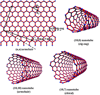 |
| | Fig. 1 Schematic representation of the relation between nanotubes and graphene. Ch = na1 + ma2 is a graphene 2D lattice vector, where a1 and a2 are unit vectors. Integers n and m uniquely define the tube diameter, chirality and metal vs. semiconducting nature. | |
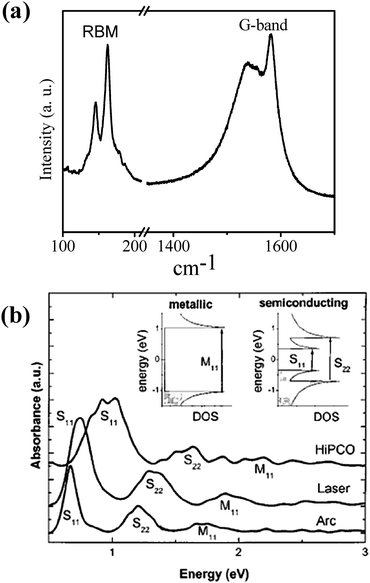
Metallic and semiconducting SWNTs are readily characterized by Raman spectroscopy and electronic spectroscopy (Fig. 2).3,12,13 The radial breathing mode (RBM) in the Raman spectra of SWNTs is useful for determining the diameter and the (n, m) values of nanotubes. Electronic properties of the nanotubes can be predicted by using the Kataura plots based on the RBM bands.13 The Raman band of SWNTs centered around 1580 cm−1 (G-band) exhibits a feature at ∼1540 cm−1 which is characteristic of metallic SWNTs (Fig. 2a). The G-band can be deconvoluted to get the relative proportions of metallic and semiconducting species. Absorption spectra of SWNTs in the visible and near-IR regions contain bands characteristic of each electronic type (Fig. 2b). A combination of Raman and electronic spectra provides an excellent means for specifying the purity and chirality aspects of the nanotubes.
The use of SWNTs in electronics, sensor technology and other areas depends on whether they are metallic or semiconducting.14 In the last few years, several methods have been devised to separate semiconducting and metallic nanotubes.15 We briefly review these methods in this article. More importantly, we shall describe methods which preferentially produce nearly pure metallic or semiconducting nanotubes. It has been found recently that metallic SWNTs can be transformed to the semiconducting species and vice versa through interaction with certain molecules or metal nanoparticles. We shall briefly examine this aspect as well. We shall also present methods employed for chirality selection and for the synthesis of junction nanotubes possessing unique electronic properties.
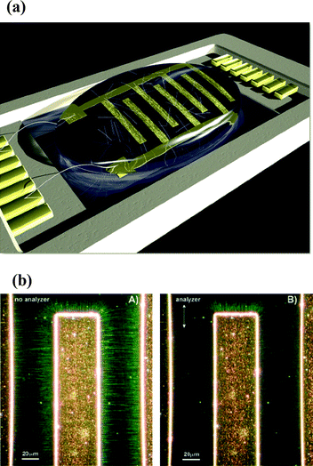
Methods to separate metallic and semiconducting SWNTs include dielectrophoresis, ultracentrifugation, and selective destruction of one type of nanotube by irradiation or by chemical means, selective interaction with molecules and covalent or noncovalent functionalization. Thus, it is possible to produce SWNTs with a narrow size distribution and specific electronic properties by density gradient ultracentrifugation in the presence of surfactants (Fig. 3).16Sucrose has been used as the gradient medium along with surfactants to obtain semiconducting SWNTs with near 95% purity.17 Making use of the differences in the relative dielectric constants of semiconducting and metallic species with respect to the solvent, alternating current dielectrophoresis has been employed to separate the two species. Fig. 4a shows the typical experimental setup for ac dielectrophoresis.18 In this study, a drop of SWNT suspension was dropped on the microelectrode array. The metallic tubes, which acquired the largest dipole moments, migrated towards the electrodes, while the semiconducting tubes remained in suspension during this process. A high degree of alignment of the tubes along the electric field lines is clearly visible from Rayleigh scattering in the green wavelength region (Fig. 4b). Selective adsorption of semiconducting nanotubes on agarose has also been used to separate metallic SWNTs.19 This involved a simple procedure wherein the gel containing SWNTs and sodium dodecyl sulfate was frozen, thawed and squeezed. The resulting solution contained 70% metallic SWNTs, leaving a gel containing 95% pure semiconducting SWNTs.
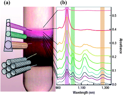 |
| | Fig. 3 Sorting SWNTs using density gradient ultracentrifugation (DGU). (a) Small-diameter (0.7–1.1 nm) SWNTs encapsulated with sodium cholate are sorted by diameter following DGU. Under these conditions, smaller-diameter SWNTs being more buoyant settle at higher points in the centrifuge tube. Larger diameter and bundled SWNTs being less buoyant settle at lower points in the centrifuge tube. The observation of visible colours in the topmost bands verifies sorting by the diameter of SWNTs. (b) Optical absorption spectra of different fractions confirm sorting by diameter (from ref. 16). | |
By making use of selective interaction of aliphatic amines with functionalized SWNTs, separation of metallic and semiconducting SWNTs has been achieved.20,21 This method seems to allow bulk separation of the two species. Raman and electronic spectra are effectively employed to investigate the effectiveness of the separation process. Preferential charge-transfer interaction of bromine with the metallic species over the semiconducting species in surfactant-stabilized SWNTs, followed by centrifugation, has been used to separate semiconducting from metallic SWNTs.22 Derivatized porphyrins selectively interact with semiconducting SWNTs through noncovalent interaction.23 Such interaction can be employed to obtain semiconducting species in solution, leaving the metallic species as residue. Photochemical osmylation has been employed to selectively react metallic SWNTs with osmium tetroxide. Subsequent self-aggregation results in the separation of the metallic and semiconducting SWNTs.24
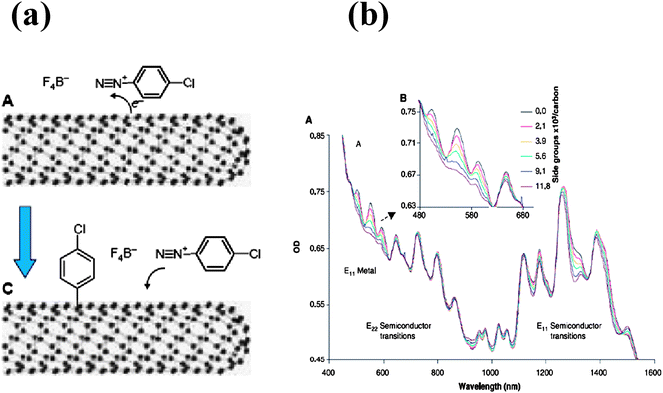
Smalley et al.25 have employed diazonium reagents for selective functionalization of metallic nanotubes with near exclusion of semiconducting nanotubes under controlled conditions (Fig. 5). Thus the hydroxybenzenediazonium salt selectively functionalizes metallic single-walled carbon nanotubes. Subsequent deprotonation in alkaline solution followed by electrophoretic separation results in the enrichment of the metallic and semiconducting fractions separately.26 Density gradient separation of the hydroxybenzenediazonium salt-functionalized SWNTs produces two distinct density fractions corresponding to functionalized metallic and pure semiconducting SWNTs. A model for the differences in the reactivities of the metallic and semiconducting nanotubes with the diazonium salt has been proposed.26 Covalent functionalization with azomethine ylides has been employed to separate metallic from semiconducting nanotubes.27,28 Wrapping SWNTs with single stranded DNA is found to depend on the tube diameter and the electronic properties of the nanotubes. This property has been used to enrich the metallic nanotubes.29
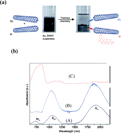
Fluorous chemistry has been effectively used to separate metallic from semiconducting nanotubes. Ghosh and Rao30 have reported effective separation of semiconducting and metallic SWNTs by employing fluorous chemistry wherein the diazonium salt of 4-heptadecafluorooctylaniline reacts preferentially with metallic SWNTs present in the mixture of nanotubes (Fig. 6). The resulting fluoro derivative was extracted in perfluorohexane leaving the semiconducting nanotubes in the aqueous layer. The products were characterized by Raman and electronic absorption spectroscopy. This method avoids the centrifugation step required by some other procedures.
In the previous section, we discussed the separation of metallic and semiconducting SWNTs. Some of the methods of separation provide procedures for the selective preparation of semiconducting and metallic SWNTs. We shall examine the procedures some of which enable a single-step synthesis of semiconducting and metallic SWNTs.
Synthesis of carbon nanotubes by the plasma-enhanced chemical vapor deposition (PECVD) method results in the preferential growth of semiconducting carbon nanotubes.31 Dai and coworkers have demonstrated the preferential growth of semiconducting SWNTs up to 90% purity by PECVD at 600 °C (Fig. 7a). The AFM and TEM images show the growth of SWNTs from the iron island. Raman spectra reveal the semiconducting nature of as grown tubes (Fig. 7b). They attribute the preferential formation of semiconducting SWNTs to the low temperature conditions which predominantly produce smaller diameter nanotubes. Qu and coworkers31c were able to grow vertically aligned semiconducting SWNTs by passing acetylene over a thin film of Fe (0.5nm) deposited on a 10 nm thick Al layer (precoated on a SiO2/Si wafer) at 750 °C. The percentage content of the semiconducting SWNTs, 96%, was obtained using combined PECVD and fast heating. High-density arrays of horizontally aligned SWNTs consisting of over 95% semiconducting nanotubes were obtained on single crystal quartz substrates by Ding et al.31d These workers proposed that introduction of methanol in the growth process, combined with the interaction between the SWNTs and the quartz lattice, leads to the selective growth of aligned semiconducting nanotubes.
 |
| | Fig. 7 (a) Schematic of the PECVD reactor. (b) SWNTs grown at 600 °C: (A) AFM image of nanotubes grown from low-density ferritin deposition on a SiO2 substrate; (B) AFM image of a tube grown from an iron-film island (nominal thickness 1 Å); (C) TEM image of an as-grown SWNT (diameter 1.2 nm); (D) left and right panels give the RBM band and the G-band respectively (from ref. 31a). | |
Gas phase reactions have been used to selectively etch out metallic nanotubes from the mixture, leaving pure semiconducting nanotubes.32 Thus, gas-phase plasma hydrocarbonation selectively etches and gasifies metallic nanotubes retaining the semiconducting nanotubes.32a Metallic nanotubes are selectively etched by hydrogen plasma as well, to yield semiconducting nanotubes in pristine form.32b
Laser irradiation of a thin film of SWNTs in air preferentially destroys metallic SWNTs.33 Metallic nanotubes in densely packed aligned SWNTs are also destroyed by xenon-lamp irradiation.34 Benzenediazonium compounds with a long alkyl chain can be used to selectively extract metallic SWNTs leaving nearly pure semiconducting nanotubes as the residue.35 The cycloaddition reaction between perfluorinated polyolefins and SWNTs eliminates metallic nanotubes,36 just as the reaction of SWNTs with fluorine gas, followed by heat treatment, selectively etches metallic SWNTs.37Hydrosilylation has been used on network-type SWNT-FET devices to selectively remove metallic SWNTs.38
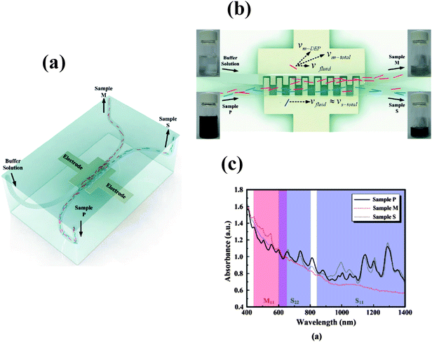
Zhang et al.39 were able to selectively etch semiconducting SWNTs by treating the mixture of SWNTs with SO3 gas at 400 °C. Metallic SWNTs could be continuously extracted from a mixture of semiconducting and metallic species in a microfluidic channel using dielectrophoretic force fields (Fig. 8).40 This is a nondestructive method yielding nearly complete selectivity. Wang et al.41 have suggested that pyrolysis of monohydroxy aliphatic alcohols with long chains on a Fe–Co/MgO catalyst results in the enrichment of metallic SWNTs. They were able to produce SWNTs enriched up to 65%. Selective etching by hydroxyl radicals of the alcohol molecules and protection of amorphous carbon might be responsible for the enrichment.
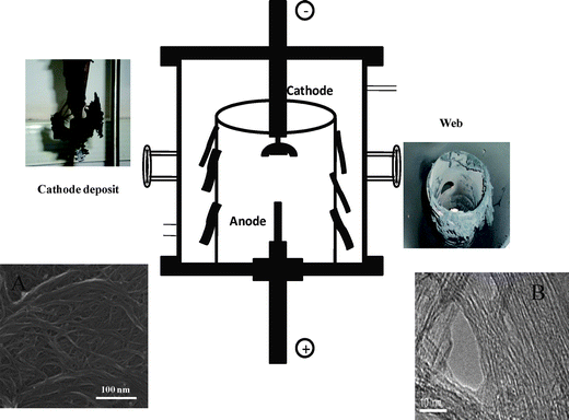
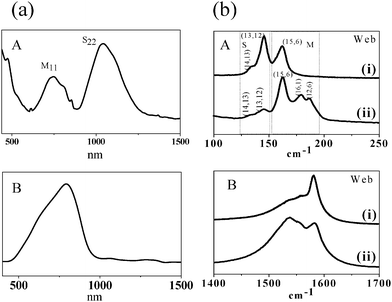
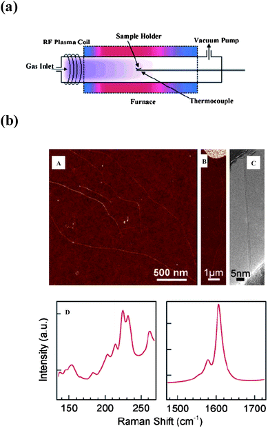
Recently, a new method has been developed by Voggu et al.42 to selectively synthesize metallic SWNTs by the arc-discharge method (Fig. 9). The method involves DC arc evaporation of a graphite rod containing the Ni + Y2O3catalyst, under a continuous flow of helium bubbled through Fe(CO)5. During the arcing process, cobweb like structures containing metallic SWNTs get deposited in the chamber. Optical absorption spectra of the deposits prepared in the presence of Fe(CO)5 show a band due to the metallic species (M11) while the bands due to the semiconducting species are nearly absent (Fig. 10a). This method can yield up to 94% pure metallic nanotubes. The formation of metallic SWNTs is also supported by Raman studies. The RBM band shows that the diameter of nanotubes changes on introducing the Fe(CO)5 vapor into the chamber leading to the formation of metallic nanotubes (Fig. 10b). One observes the broadening of the Breit-Wagner Fano peak of the metallic nanotubes in the spectrum. The sheet resistance of the SWNTs from the walls of the arc chamber formed in the presence of Fe(CO)5 was much lower than that of SWNTs obtained in the absence of Fe(CO)5. This method can be used for the bulk synthesis of enriched metallic SWNTs.
Metal ↔ semiconductor transitions induced by molecular interaction
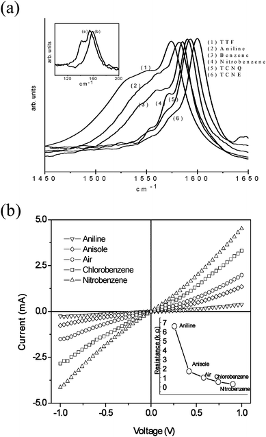
SWNTs interact with electron donor and acceptor molecules as evidenced by the changes in the Raman spectra and electronic properties. It has been shown that electron donor and acceptor molecules such as nitrobenzene, aniline, tetracyanoethylene (TCNE) and tetrathiafulvalene (TTF) alter the electronic structure of SWNTs.43a,44 The feature due to the metallic species around 1540 cm−1 in the G-band of the Raman spectrum nearly disappears on interaction of SWNTs with electron acceptors such as nitrobenzene and TCNE whereas interaction of electron donors such as aniline and TTF with SWNTs increases the metallic feature (Fig. 11a).43a It appears that electron donor molecules interact selectively with semiconducting SWNTs whereas electron acceptors molecules interact with metallic SWNTs giving rise to metal ↔ semiconductor transitions. The changes in the Raman spectra are accompanied by changes in the electrical resistivity (Fig. 11b). It has been found that nanoparticles of gold and platinum deposited on SWNTs also transform the semiconducting SWNTs to the metallic species due to Columbic charge transfer.43b Metal to semiconductor transition in SWNTs has been induced by helical wrapping of DNA.45Water appears to be critical for this reversible transition which is accompanied by hybrid formation with DNA. It is predicted that a band gap can open up in metallic SWNTs wrapped with ssDNA in the presence of water molecules, due to charge transfer.
Chirality selection
SWNTs samples prepared by most of the methods consist of nanotubes with different n and m values. The various (n,m) combinations could be very large and it is therefore desirable to achieve chirality selection of SWNTs by an appropriate method. In this respect, DNA is effective in dispersing SWNTs and also in chirality fractionation according to the diameter and metallicity by using post-solubilization separation techniques, such as ion exchange and density gradient separation.46 Kim et al.47 have described a solubilization cum separation method by using genomic DNA which exfoliates and disperses nanotubes and selectively enriches (6,5) nanotubes as compared to (10,6) tubes. Theoretical studies of SWNTs wrapped with flavin mononucleotide predict specific enrichment of (8,6) nanotubes.48
A bimetallic Fe–Ru catalyst is shown to give rise to SWNTs with narrow diameter and chirality distribution in a methane CVD reaction.44 At 600 °C, SWNTs enriched in (6,5) tubes are obtained while at 850 °C polydisperse samples consisting of (8,4), (7,6) and (7,5) tubes are obtained. It has been possible to enrich (8,4) tubes, free of metallic species, by ion exchange chromatography.49 The (n,m) distribution of SWNTs can also be controlled by gas feed composition, the reactant temperature and the type of catalyst.50 By using CO as a feed over CoMo/SiO2catalysts, an increase in nanotube diameter is observed on increasing the temperature, without any change in the chiral angles. By changing the support from SiO2 to MgO, nanotubes with a similar diameter but different chiral angles are obtained. Varying the composition of the gaseous feed under the same reaction conditions gives rise to different (n,m) distributions. A narrow (n,m) distribution seems to be obtained under high-pressure CO or vacuumed C2H5OH and CH3OH on a Co–Mo catalyst.51 Wang et al.52 have reported selective growth of bulk SWNTs enriched with three different dominant chiralities including (6,5), (7,5), and (7,6) through the adjustment of the pressure of CO on Co–Mo catalysts from 2 to 18 bar. Optically active SWNTs are obtained by the extraction of right- or left-handed SWNTs by using chiral diporphyrin molecules which act as chiral nanotweezers (Fig. 12). The porphyrin molecules are readily removed after reaction.53 By using open ended SWNTs as seeds, SWNT clones can be obtained. This method may be useful for chiral selective growth of specific nanotubes.54
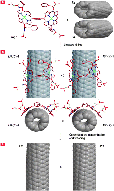 |
| | Fig. 12 Schematic of the separation of left-handed (LH) and right-handed (RH) SWNTs with a chiral diporphyrin, (S)-1. (a) A commercial sample of SWNTs containing left- and right-handed helical isomers is suspended in a methanol solution containing the (S)-1 nanotweezers. (b) After treatment in an ultrasound bath, some SWNTs are solubilized by forming complexes with multiple copies of the nanotweezers. Energy minimized structures of the complexes LH:(S)-1 and RH:(S)-1, obtained from a comprehensive molecular mechanics calculation, indicate that the right-handed nanotubes form stronger complexes and are solubilized in larger amounts than the left-handed ones. (c) After centrifugation and collection of the supernatant liquid, the samples can be concentrated to give a solid. The nanotweezers are removed by washing with THF and pyridinesolvents to leave free carbon nanotubes, and there are more right-handed ones than left-handed because of the differential solubilization in the previous step. Although only the most abundant (6,5)-SWNTs are shown in this figure, other chiral indices such as (7,5), (7,6), (8,4) and (8,3) are also included in the samples and their mirror image forms are extracted in a similar manner (from ref. 53a). | |
Synthesis of junction carbon nanotubes has been an important challenge. Earlier efforts focused on the generation of multi-walled carbon nanotubes by using template methods.66 To obtain large yields of branched CNTs, the most used route is to introduce additives such as thiophene in the reactants. This was first reported by Rao et al. in 2000.67MWNT junctions were produced by the pyrolysis of nickelocene (which acts as both the catalyst source and the carbon feedstock) in the presence of thiophene (Fig. 13a, b). The products contained branched MWNTs up to 70%. They observed asymmetry in the I–V curve at the Y-junction whereas it was linear along the arms (Fig. 13c). A similar CVD process with different additives has been employed to generate branched MWNTs.68 The role of sulfur (thiophene) in the branching process of nanotubes with stacked-cone morphologies has been explained.69 The growing branches appear to possess a minute amount of sulfur which is sufficient to promote the formation of heptagons (negative curvature) and pentagons (positive curvature).
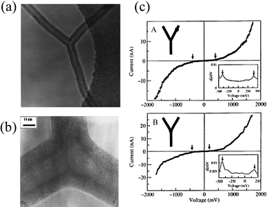 |
| | Fig. 13 (a) A typical TEM image of a Y-junction nanotube, (b) HREM image of a Y-junction showing the fishbone-type stacking of graphene sheets and (c) I–V curves collected from different points in a Y-junction carbon nanotube; (A) from one of the arms away from the junction and (B) from the junction of the three arms. Insets show plots of dI/dV vs. bias voltage. The observed gaps are indicated by arrows (from ref. 67a). | |
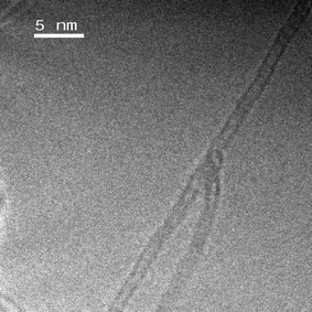
Due to the advantages of multiterminal SWNTs over MWNTs in applications, there have been efforts to prepare Y-junction SWNTs. Y-Junction SWNTs were seen in STM samples produced by the thermal decomposition of C60 in the presence of transition metals like Ti, Cr, Fe, Co and Ni.70 Choi and coworkers71 synthesized Y-junction SWNTs using thermal chemical vapor deposition of methane over Mo or Zr doped Fe nanoparticles supported on aluminium oxide. The presence of Mo or Zr in the Fe catalyst enhances the nucleation and growth of carbon nanotubes, and facilitates the growth of new nanotube branches when they are attached to the sidewalls of the existing nanotubes. Voggu et al.72 have prepared Y-junction SWNTs by carrying out arc discharge of graphite over a Ni–Y2O3catalyst in an atmosphere of thiophene and helium (Fig. 14).
Conclusions
The previous sections clearly bring out the progress made in selectively generating metallic, semiconducting and other types of single-walled carbon nanotubes with unique electronic properties. The problems are not entirely solved. There is a need for easy procedures for routine synthesis of bulk quantities of monodisperse metallic and semiconducting SWNTs. Use of SWNTs for applications in nanoelectronics, sensor technologies and other areas will be greatly facilitated by such procedures. It would be most useful if one can tailor-make SWNTs with the desired (n,m) values. The discovery of metal-semiconductor and semiconductor-metal transitions in SWNTs brought about by interaction with electron acceptor and donor molecules is of great interest and may find useful applications. We do not yet have a well-defined procedure to prepare Y-junction SWNTs in bulk. This could be of value in nanoelectronics since Y-junction SWNTs can be used as veritable chips.
References
- S. Iijima, Nature, 1991, 354, 56 CrossRef CAS.
-
(a)
R. Saito, G. Dresselhaus and M. S. Dresselhaus, Physical Properties of Carbon Nanotubes (Imperial College Press, London), 1998 Search PubMed;
(b) P. Avouris, Acc. Chem. Res., 2002, 35, 1026 CrossRef CAS.
-
(a)
C. N. R. Rao and A. Govindaraj, Nanotubes and Nanowires, RSC Nanoscience & Nanotechnology series, Royal Society of Chemistry, Cambridge, 2005 Search PubMed;
(b)
Nanomaterials Chemistry: Recent Developments and New Directions, Eds. C. N. R. Rao, A. Müller and A. K. Cheetham, Wiley-VCH, Weinheim, 2007 Search PubMed.
-
(a) R. E. Smalley, Y. Li, V. C. Moore, B. K. Price, R. Colorado, Jr., H. K. Schmidt, R. H. Hauge, A. R. Barron and J. M. Tour, J. Am. Chem. Soc., 2006, 128, 15824 CrossRef CAS;
(b) A. G. Nasibulin, D. P. Brown, P. Queipo, D. Gonzalez, H. Jiang and E. I. Kauppinen, Chem. Phys. Lett., 2006, 417, 179 CrossRef CAS;
(c) M. Keidar, I. Levchenko, T. Arbel, M. Alexander, A. M. Waas and K. Ostrikov, Appl. Phys. Lett., 2008, 92, 043129 CrossRef;
(d) S. Chakrabarti, H. Kume, L. Pan, T. Nagasaka and Y. Nakayama, J. Phys. Chem. C, 2007, 111, 1929 CrossRef;
(e) H. Zhang, G. Cao, Z. Wang, Y. Yang, Z. Shi and Z. Gu, J. Phys. Chem. C, 2008, 112, 12706 CrossRef CAS.
-
(a) J. Lu, D. Yuan, J. Liu, W. Leng and T. E. Kopley, Nano Lett., 2008, 8, 3325 CrossRef CAS;
(b) C. L. Pint, S. T. Pheasant, M. Pasquali, K. E. Coulter, H. K. Schmidt and R. H. Hauge, Nano Lett., 2008, 8, 1879 CrossRef CAS;
(c) T. Saito, S. Ohshima, T. Okazaki, S. Ohmori, M. Yumura and S. Iijima, J. Nanosci. Nanotechnol., 2008, 8, 6153 CrossRef CAS;
(d) Y. Wang, Y. Q. Liu, D. C. Wi, L. C. Cao, L. Fu, X. L. Li, H. Kajiura, Y. M. Li and K. Noda, J. Mater. Chem., 2007, 17, 357 RSC;
(e) D. Kondo, S. Sato and Y. Awano, Chem. Phys. Lett., 2006, 422, 481 CrossRef CAS;
(f) W. L. Wang, X. D. Bai, Z. Xu, S. Liu and E. G. Wang, Chem. Phys. Lett., 2006, 419, 81 CrossRef CAS;
(g) M. Bystrzejewski, R. Schonfelder, G. Cuniberti, H. Lange, A. Huczko, T. Gemming, T. Pichler, B. Buchner and M. Rummeli, Chem. Mater., 2008, 20, 6586 CrossRef CAS.
-
(a) L. Song, L. Ci, L. Sun, C. Jin, L. Liu, W. Ma, D. Liu, X. Zhao, S. Luo, Z. Zhang, Y. Xiang, J. Zhou, W. Zhou, Y. Ding, Z. Wang and S. Xie, Adv. Mater., 2006, 18, 1817 CrossRef CAS;
(b) D. Grimm, P. Venezuela, F. Banhart, N. Grobert, H. Terrones, P. M. Ajayan, M. Terrones and A. Latge, Small, 2007, 3, 1900 CrossRef CAS.
- S. Chakrabarti, T. Nagasaka, Y. Yoshikawa, L. Pan and Y. Nakayama, Jpn. J. Appl. Phys., 2006, 45, L720 CrossRef CAS.
- T. H. Li, Y. M. Zhao, M. Roe, D. Furniss, Y. Q. Zhu, S. Ravi, P. Silva, J. Q. Wei, D. H. Wu and C. H. P. Poa, Small, 2006, 2, 1026 CrossRef CAS.
-
(a) D. Kondo, S. Sato, A. Kawabata and Y. Awano, Nanotechnology, 2008, 19, 435601 CrossRef;
(b) L. Qu, F. Du and L. Dai, Nano Lett., 2008, 8, 2682 CrossRef CAS;
(c) Y. Taki, M. Kikuchi, K. Shinohara and A. Tanaka, Jpn. J. Appl. Phys., 2008, 47, 721 CrossRef CAS;
(d) E. Einarsson, H. Shiozawa, C. Kramberger, M. H. Rummeli, A. Gruneis, T. Pichler and S. Maruyama, J. Phys. Chem. C, 2007, 111, 17861 CrossRef CAS;
(e) L. Zhang, Y. Tan and E. Resasco, Chem. Phys. Lett., 2006, 422, 198 CrossRef CAS;
(f) D. H. Lee, W. J. Lee and S. O. Kim, Chem. Mater., 2009, 21, 1368 CrossRef CAS.
-
(a) C. Kocabas, M. Shim and J. A. Roger, J. Am. Chem. Soc., 2006, 128, 4540 CrossRef CAS;
(b) C. Kocabas, S. J. Kang, T. Ozel, M. Shim and J. A. Rogers, J. Phys. Chem. C, 2007, 111, 17879 CrossRef CAS;
(c) N. Yoshihara, H. Ago, K. Imamoto, M. Tsuji, T. Ikuta and K. Takashashi, J. Phys. Chem. C, 2009, 113, 8030 CrossRef CAS.
-
(a) M. C. Hersam, Nat. Nanotechnol., 2008, 3, 387 Search PubMed;
(b) S. Niyogi, C. G. Demsmore and S. K. Doorn, J. Am. Chem. Soc., 2009, 131, 1144 CrossRef CAS;
(c) R. M. Tromp, A. Afzali, M. Freitag, D. B. Mitzi and Zh. Chen, Nano Lett., 2008, 8, 469 CrossRef CAS;
(d) H. Yang, S. C. Wang, P. Mercier and D. L. Akins, Chem. Commun., 2006, 1425 RSC.
-
(a) M. S. Dresselhaus and P. C. Eklund, Adv. Phys., 2000, 49, 705 CrossRef CAS;
(b) M. S. Dresselhaus, G. Dresselhaus and A. Jorio, J. Phys. Chem. C, 2007, 111, 17887 CrossRef CAS;
(c) M. S. Dresselhaus, G. Dresselhaus, A. Jorio, A. G. S. Filho and R. Saito, Carbon, 2002, 40, 2043 CrossRef CAS.
-
(a) H. Kataura, Y. Kumazawa, Y. Maniwaa, I. Umezu, S. Six, Y. Ohtsuka and Y. Achiba, Synth. Met., 1999, 103, 2555 CrossRef CAS;
(b) M. S. Strano, J. Am. Chem. Soc., 2003, 125, 16148 CrossRef CAS;
(c) M. A. Hamon, M. E. Itkis, S. Niyogi, T. Alvaraez, C. Kuper, M. Menon and R. C. Haddon, J. Am. Chem. Soc., 2001, 123, 11292 CrossRef CAS.
-
(a) M. Lee, J. Im, B. Y. Lee, S. Myung, J. Kang, L. Huang, Y. K. Kwon and S. Hong, Nat. Nanotechnol., 2006, 1, 66 Search PubMed;
(b) P. G. Collins, M. S. Arnold and P. Avouris, Science, 2001, 292, 706 CrossRef;
(c) S. G. Rao, L. Huang, W. Setyawan and S. Hong, Nature, 2003, 425, 36 CrossRef CAS;
(d) J. A. Misewich, R. Martel, P. Avouris, J. C. Tsang, S. Heinze and J. Tersoff, Science, 2003, 300, 783 CrossRef CAS.
-
(a) S. Campidelli, M. Meneghetti and M. Prato, Small, 2007, 3, 1672 CrossRef CAS;
(b) M. C. Hersam, Nat. Nanotechnol., 2008, 3, 387 Search PubMed.
- M. S. Arnold, A. A. Green, J. F. Hulvat, S. I. Stupp and M. C. Hersam, Nat. Nanotechnol., 2006, 1, 60 Search PubMed.
- K. Yanagi, T. Iituka, S. Fujii and H. Kataura, J. Phys. Chem. C, 2008, 112, 18889 CAS.
- R. Krupke, F. Henrich, H.v. Lohneysen and M. M. Kappes, Science, 2003, 301, 344 CrossRef CAS.
- T. Tanaka, H. Jin, Y. Miyata, S. Fujii, H. Suga, Y. Naitoh, T. Minari, R. Miyadera, K. Tsukagoshi and H. Katura, Nano Lett., 2009, 9, 1497 CrossRef CAS.
-
(a) D. Chattopadhyay, I. Galeska and F. Papadimitrakopoulos, J. Am. Chem. Soc., 2003, 125, 3370 CrossRef CAS;
(b) S. Y. Ju, M. Utz and F. Papadimitrakopoulos, J. Am. Chem. Soc., 2009, 131, 6775 CrossRef CAS.
-
(a) G. G. Samsonidze, S. G. Chou, A. P. Santos, V. W. Brar, G. Dresselhaus, M. S. Dresselhaus, A. Selbst, A. K. Swan, M. S. Unlu, B. B. Goldberg, D. Chattopadyay, S. N. Kim and F. Papadimitrakopoulos, Appl. Phys. Lett., 2004, 85, 1006 CrossRef CAS;
(b) Y. Maeda, M. Kanda, M. Hashimoto, T. Hasegawa, S. Kimura, Y. Lian, T. Wakahara, T. Akasaka, S. Kazaoui, N. Minami, T. Okazaki, Y. Hayamizu, H. Hata, J. Lu and S. Nagase, J. Am. Chem. Soc., 2006, 128, 12239 CrossRef CAS.
- Z. Chen, X. Du, M. H. Du, C. D. Rancken, H. P. Cheng and A. G. Rinzler, Nano Lett., 2003, 3, 1245 CrossRef CAS.
- H. Li, B. Zhou, Y. Lin, L. Gu, W. Wang, K. A. S. Fernando, S. Kumar, L. F. Allard and Y. P. Sun, J. Am. Chem. Soc., 2004, 126, 1014 CrossRef CAS.
- S. Banerjee and S. S. Wong, J. Am. Chem. Soc., 2004, 126, 2073 CrossRef CAS.
- M. S. Strano, C. A. Dyke, M. L. Usrey, P. W. Barone, M. J. Allen, H. Shan, C. Kittrell, R. H. Hauge, J. M. Tour and R. E. Smalley, Science, 2003, 301, 1519 CrossRef CAS.
-
(a) W. J. Kim, M. L. Usrey and M. S. Strano, Chem. Mater., 2007, 19, 1571 CrossRef CAS;
(b) W. J. Kim, N. Nair, C. Y. Lee and M. S. Strano, J. Phys. Chem. C, 2008, 112, 7326 CrossRef CAS.
- V. Georgakilas, K. Kordatos, M. Prato, D. M. Guldi, M. Holzinger and A. Hirsch, J. Am. Chem. Soc., 2002, 124, 760 CrossRef CAS.
- C. M. Ménard-Moyon, N. Izard, E. Doris and C. Mioskowski, J. Am. Chem. Soc., 2006, 128, 6552 CrossRef CAS.
- M. Zheng, A. Jagota, M. S. Strano, A. P. Santos, P. Barone, S. G. Chou, B. A. Diner, M. S. Dresselhaus, R. S. Mclean, G. B. Onoa, G. G. Samsonidze, E. D. Semke, M. Usrey and D. J. Walls, Science, 2003, 302, 1545 CrossRef CAS.
- S. Ghosh and C. N. R. Rao, Nano Res., 2009, 2, 183 Search PubMed.
-
(a) Y. Li, D. Mann, M. Rolandi, W. Kim, A. Ural, S. Hung, A. Javery, J. Cao, D. Wang, E. Yenilmez, Q. Wang, H. F. Gibbons, Y. Nishi and H. Dai, Nano Lett., 2004, 4, 317 CrossRef CAS;
(b) Y. Li, S. Peng, D. Mann, R. Tu, K. J. Cho and H. Dai, J. Phys. Chem. B, 2005, 109, 6968 CrossRef CAS;
(c) L. Qu, F. Du and L. Dai, Nano Lett., 2008, 8, 2682 CrossRef CAS;
(d) L. Ding, A. Tselev, J. Wang, D. Yuan, H. Chu, T. P. McNicholas, Y. Li and J. Liu, Nano Lett., 2009, 9, 800 CrossRef CAS.
-
(a) G. Zhang, P. Qi, X. Wang, Y. Lu, X. Li, R. Tu, S. Bangsaruntip, D. Mann, L. Zhang and H. Dai, Science, 2006, 314, 974 CrossRef CAS;
(b) A. Hassanien, M. Tokumoto, P. Umek, D. Vrbanic, M. Mozetic, D. Mihailvoi, P. Veturini and S. Pejovnik, Nanotechnology, 2005, 16, 278 CrossRef CAS.
- H. Huang, R. Maruyama, K. Noda, H. Kajiura and K. Kadono, J. Phys. Chem. B, 2006, 110, 7316 CrossRef CAS.
- Y. Zhang, Y. Zhang, X. Xian, J. Zhang and Z. Liu, J. Phys. Chem. C, 2008, 112, 3849 CrossRef CAS.
- S. Toyoda, Y. Yamaguchi, M. Hiwatashi, Y. Tomonari, H. Murakami and N. Nakashima, Chem.–Asian J., 2007, 2, 147.
- M. Kanungo, H. Lu, G. G. Malliaras and G. B. Blanchet, Science, 2009, 323, 234 CrossRef CAS.
- C. M. Yang, K. H. An, J. S. Park, K. A. Park, S. C. Lim, S. H. Cho, Y. S. Lee, W. park, C. Y. Park and Y. H. Lee, Phys. Rev. B: Condens. Matter Mater. Phys., 2006, 73, 075419 CrossRef.
- Y. Lee, K.-S. Jeon, H. Lim, H. S. Shin, S. M. Jin, H. R. Byon, Y. D. Suh and H. C. Choi, Small, 2009, 5, 1398 CrossRef CAS.
- H. Zhang, Y. Liu, L. Cao, D. Weo, Y. Wang, H. Kajiura, Y. Li, K. Noda, G. Luo, L. Wang, J. Zhou, L. Lu and Z. Gao, Adv. Mater., 2009, 21, 813 CrossRef CAS.
- D. H. Shin, J. E. Kim, H. C. Shim, J. W. Song, J. H. Yoon, J. Kim, S. Jeong, J. Kang, S. Baik and C. S. Han, Nano Lett., 2008, 8, 4380 CrossRef CAS.
- Y. Wang, Y. Liu, X. Li, L. Cao, D. Wei, H. Zhang, D. Shi, G. Yu, H. Kajiura and Y. Li, Small, 2007, 3, 1486 CrossRef CAS.
-
(a)
R. Voggu, A. Govindaraj and C. N. R. Rao, arXiv: cond-mat/0903.5359;
(b)
R. Voggu, S. Ghosh, A. Govindaraj and C. N. R. Rao, J. Nanosci. Nanotechnol., in press Search PubMed.
-
(a) R. Voggu, C. S. Rout, A. D. Franklin, T. S. Fisher and C. N. R. Rao, J. Phys. Chem. C, 2008, 112, 13053 CrossRef CAS;
(b) R. Voggu, S. Pal, S. K. Pati and C. N. R. Rao, J. Phys.: Condens. Matter, 2008, 20, 215211 CrossRef.
- H. Shin, S. M. Kim, S. M. Yoon, A. Benayad, K. K. Kim, S. J. Kim, H. K. Park, J. Y. Choi and Y. H. Lee, J. Am. Chem. Soc., 2008, 130, 2062 CrossRef CAS.
- M. Cha, S. Jung, M. H. Cha, G. Kim, J. Ihm and J. Lee, Nano Lett., 2009, 9, 1345 CrossRef CAS.
-
(a) M. Zheng, A. Jagota, M. S. Strano, A. P. Santos, P. Barone, S. G. Chou, B. A. Diner, M. S. Dresselhaus, R. S. Mclean, G. B. Onoa, G. G. Samsonidze, E. D. Semke, M. Usrey and D. J. Walls, Science, 2003, 302, 1545 CrossRef CAS;
(b) M. Zheng and E. D. Semke, J. Am. Chem. Soc., 2007, 129, 6084 CrossRef CAS;
(c) M. S. Arnold, S. I. Stupp and Mark C. Hersam, Nano Lett., 2005, 5, 713 CrossRef CAS.
- S. N. Kim, Z. Kuang, J. G. Grote, B. L. Farmer and R. R. Naik, Nano Lett., 2008, 8, 4415 CrossRef CAS.
- O. Ogunro and X. Q. Wang, Nano Lett., 2009, 9, 1034 CrossRef CAS.
- X. Li, X. Tu, S. Zaric, K. Welsher, W. S. Seo, W. Zhao and H. Dai, J. Am. Chem. Soc., 2007, 129, 15770 CrossRef CAS.
- G. Lolli, L. Zhang, L. Balzano, N. Sakulchaicharoen, Y. Tan and D. E. Resasco, J. Phys. Chem. B, 2006, 110, 2108 CrossRef CAS.
- B. Wang, C. H. P. Poa, L. Wei, L. J. Li, Y. Yang and Y. Chen, J. Am. Chem. Soc., 2007, 129, 9014 CrossRef CAS.
- B. Wang, L. Wei, L. Yao, L. J. Li, Y. Yang and Y. Chen, J. Phys. Chem. C, 2007, 111, 14612 CrossRef CAS.
-
(a) X. Peng, N. Komatsu, S. Bhattacharya, T. Shimawaki, S. Aonuma, T. Kimura and A. Osuka, Nat. Nanotechnol., 2007, 2, 361 Search PubMed;
(b) X. Peng, N. Komatsu, T. Kimura and A. Osuka, ACS Nano, 2008, 2, 2045 CrossRef CAS.
- Y. Yao, C. Feng, J. Zhang and Z. Liu, Nano Lett., 2009, 9, 1673 CrossRef CAS.
- A. N. Andriotis, M. Menon, D. Srivastava and L. Chernozatonskii, Phys. Rev. B: Condens. Matter Mater. Phys., 2002, 65, 165416 CrossRef.
- A. N. Andriotis, M. Menon, D. Srivastava and L. Chernozatonskii, Phys. Rev. Lett., 2001, 87, 066802 CrossRef CAS.
- A. N. Andriotis and M. Menon, Appl. Phys. Lett., 2001, 79, 266 CrossRef CAS.
- Z. Yao, H. W. C. Postma, L. Balents and C. Dekker, Nature, 1999, 402, 273 CrossRef CAS.
- Y. G. Yao, Q. W. Li, J. Zhang, R. Liu, L. Y. Jiao, Y. T. Zhu and Z. F. Liu, Nat. Mater., 2007, 6, 283 CAS.
- C. W. Zhou, J. Kong, E. Yenilmez and H. J. Dai, Science, 2000, 290, 1552 CrossRef CAS.
- P. R. Bandaru, C. Daraio, S. Jin and A. M. Rao, Nat. Mater., 2005, 4, 663 CrossRef CAS.
-
(a) M. Ouyang, J. L. Huang, C. L. Cheung and C. M. Lieber, Science, 2001, 291, 97 CrossRef CAS;
(b) H. Kim, J. Lee, Y. J. Song, B. Y. Choi, S. J. Kahng and Y. Kuk, Thin Solid Films, 2004, 464–465, 335 CrossRef CAS.
-
(a) S. K. Doorn, M. J. Oconnell, L. X. Zheng, Y. T. Zhu, S. M. Huang and J. Liu, Phys. Rev. Lett., 2005, 94, 016802 CrossRef;
(b) J. Han, M. P. Anantram, R. L. Jaffe, J. Kong and H. J. Dai, Phys. Rev. B: Condens. Matter Mater. Phys., 1998, 57, 14983 CrossRef CAS.
- A. Hassanien, M. Holzinger, A. Hirsch, M. Tokumoto and P. Venturini, Synth. Met., 2003, 137, 1203 CrossRef CAS.
-
(a) Y. G. Yao, Q. W. Li, J. Zhang, R. Liu, L. Y. Jiao, Y. T. Zhu and Z. F. Liu, Nat. Mater., 2007, 6, 283 CAS;
(b) Y. G. Yao, R. Liu, J. Zhang, L. Y. Jiao and Z. F. Liu, J. Phys. Chem. B, 2007, 111, 8407 CAS.
- J. Li, C. Papadopoulos and J. Xu, Nature, 1999, 402, 253 CAS.
-
(a) B. C. Satishkumar, P. J. Thomas, A. Govindaraj and C. N. R. Rao, Appl. Phys. Lett., 2000, 77, 2530 CrossRef CAS;
(b) F. L. Deepak, N. S. John, A. Govindaraj, G. U. Kulkarni and C. N. R. Rao, Chem. Phys. Lett., 2005, 411, 468 CrossRef CAS.
-
(a) F. L. Deepak, A. Govindaraj and C. N. R. Rao, Chem. Phys. Lett., 2001, 345, 5 CrossRef CAS;
(b) S. M. Huang, L. M. Dai and A. Mau, Phys. B, 2002, 323, 336 CrossRef CAS.
- J. M. Romo-Herrera, B. G. Sumpter, D. A. Cullen, H. Terrones, E. Cruz-Silva, D. J. Smith, V. Meunier and M. Terrones, Angew. Chem., Int. Ed., 2008, 47, 2948 CrossRef CAS.
-
(a) P. Nagy, R. Ehlich, L. P. Biró and J. Gyulai, Appl. Phys. A: Mater. Sci. Process., 2000, 70, 481 CrossRef CAS;
(b) L. P. Biró, R. Ehlich, Z. Osváth, A. Koós, Z. E. Horváth, J. Gyulai and J. B. Nagy, Phys. Rev. Lett., 2002, 89, 075505 CrossRef CAS;
(c) L. P. Biró, R. Ehlich, Z. Osvath, A. Koos, Z. E. Horvath, J. Gyulai and J. B. Nagy, Mater. Sci. Eng., C, 2002, 19, 3 CrossRef;
(d) L. P. Biró, R. Ehlich, Z. Osvath, A. Koos, Z. E. Horvath, J. Gyulai and J. B. Nagy, Diamond Relat. Mater., 2002, 11, 1081 CrossRef CAS.
-
(a) Y. C. Choi and W. Choi, Carbon, 2005, 43, 2737 CrossRef CAS;
(b) J. Huang, D. H. Kim, R. Seelaboyina, B. K. Rao, D. Wang, M. Park and W. Choi, Diamond Relat. Mater., 2007, 16, 1524 CrossRef CAS;
(c) D. H. Kim, J. Huang, H. K. Shin, S. Roy and W. Choi, Nano Lett., 2006, 6, 2821 CrossRef CAS;
(d) D. H. Kim, J. Huang, B. K. Rao and W. Choi, J. Appl. Phys., 2006, 99, 0561.
-
R. Voggu, Md. Ikram, A. Govindaraj and C. N. R. Rao, to be published.
|
| This journal is © The Royal Society of Chemistry 2009 |
Click here to see how this site uses Cookies. View our privacy policy here.