Nanostructured Pt decorated graphene and multi walled carbon nanotube based room temperature hydrogen gas sensor
Adarsh
Kaniyoor
,
R.
Imran Jafri
,
T.
Arockiadoss
and
S.
Ramaprabhu
*
Alternative Energy and Nanotechnology Laboratory (AENL), Nano Functional Materials Technology Centre (NFMTC), Department of Physics, Indian Institute of Technology Madras, Chennai, 600036, India. E-mail: ramp@iitm.ac.in
First published on 29th September 2009
Abstract
Herein, we report the fabrication of hydrogen gas sensors based on noble nanometal decorated one dimensional multi walled carbon nanotubes and two dimensional graphene by a simple drop casting technique, with practical applications in view. Pt decorated functionalized graphene sheets (Pt/f-G) and Pt decorated functionalized multi walled carbon nanotubes (Pt/f-MWNT) were synthesized and employed as hydrogen sensors. Systematic investigation of hydrogen sensing, at a low detection level of 4 vol% hydrogen in air, of (Pt/f-G) reveals a response time comparable to that of (Pt/f-MWNT) but with a two fold increase in the sensitivity at room temperature. These sensors were also found to be stable over repeated cycles of hydrogenation and dehydrogenation.
1. Introduction
Hydrogen energy is showing promise as clean energy for future applications. However, since hydrogen gas is odorless, colorless and highly inflammable, safety becomes a primary concern. Hydrogen concentration in excess of 4 vol% in ambient air is potentially explosive.1,2 Thus, the necessity of hydrogen sensors for leak detection as well as H2 line feed monitoring arises. Measurable response to hydrogen and room temperature operating conditions are some of the prerequisites for good hydrogen sensing materials. Noble metal and metal oxide based sensors are already in the market.3,4 While the metal oxide sensors have the drawback of elevated operating temperatures, the bulk Pd and Pt based sensors, though very efficient, are expensive. This problem is circumvented by using nano sized powders, films or by depositing these particles on other nanostructures with larger surface area. In this context, carbon based nanostructured materials can be highly useful due to their large surface area and high electrical conductivity.Carbon based nanostructured materials, especially the one dimensional carbon nanotubes5 and of late even the two dimensional graphene6 have been of tremendous scientific and technological interest due to their unique physical and chemical properties.7,8 The electronic properties of the multi walled carbon nanotubes (MWNT) are governed mainly by the outermost layer which is also chemically very active. In addition, their 1D nature gives them a large surface area. Graphene, on the other hand is a planar sheet of graphitic carbon wherein the carbon atoms are tightly arranged in a 2D honeycomb like lattice. Graphene sheets have extremely large surface areas, approximately 2 times that of MWNT. Moreover, exceptionally high electron mobilities at room temperatures have been reported for multi layer graphene, with values in excess of 10![[thin space (1/6-em)]](https://www.rsc.org/images/entities/char_2009.gif) 000 cm2 V−1 s−1. More importantly, both these carbon nanostructures can be engineered to detect suitable gases by the introduction of defects and functional groups, thus making them suitable candidates for gas sensing applications. It is known that Pt is a very good material for H2 sensing because Pt dissociates H2 molecules in to H atoms. Due to their large surface area, the carbon nanostructures are used as support materials for dispersing of Ptnanoparticles uniformly on surfaces mainly to reduce the Pt content. In addition, carbon nanotubes and graphene are highly conducting materials which will enhance the detection of the change in the electrical properties due to adsorption of hydrogen.
000 cm2 V−1 s−1. More importantly, both these carbon nanostructures can be engineered to detect suitable gases by the introduction of defects and functional groups, thus making them suitable candidates for gas sensing applications. It is known that Pt is a very good material for H2 sensing because Pt dissociates H2 molecules in to H atoms. Due to their large surface area, the carbon nanostructures are used as support materials for dispersing of Ptnanoparticles uniformly on surfaces mainly to reduce the Pt content. In addition, carbon nanotubes and graphene are highly conducting materials which will enhance the detection of the change in the electrical properties due to adsorption of hydrogen.
With these things in view, the current work focuses on developing room temperature hydrogen gas sensors based on Pt decorated functionalized graphene sheets (Pt/f-G) and Pt decorated functionalized multi walled carbon nanotubes (Pt/f-MWNT). Keeping large scale applications in view, we have employed a simple drop casting technique for the fabrication of these sensors. The Pt/f-MWNT sensor prepared this way shows a performance comparable to a spin coated Pt/f-MWNT sensor reported by us in an earlier work,9 thus justifying the procedure. Additionally, for flow monitoring of hydrogen gas as in hydrogen fuel stations, hydrogen pipelines etc. detection of large volumes of gas becomes necessary. Hence the detection levels were maintained in terms of volume %.
2. Experimental details
2.1 Synthesis of carbon nanostructures
MWNT were synthesized and purified according to procedures reported by us previously.10 Briefly, MWNT were prepared by catalytic chemical vapour deposition technique (CCVD) over rare earth based AB3 alloy hydride catalyst using acetylene gas as the carbon precursor. The purification involved air oxidation to remove carbonaceous impurities, followed by acid treatment to remove catalyst particles. For further functionalization the purified samples were refluxed with conc. nitric acid for 24 h at 80 °C, followed by washing, filtering and drying. The final product was labeled ‘f-MWNT’.Graphene sheets were synthesized by thermal exfoliation of graphitic oxide, as reported by Schniepp et al.11 In short, graphitic oxide was prepared by treating graphite with an oxidizing solution of conc. sulfuric acid and nitric acid. Potassium chlorate was added slowly over a period of 15 min. The reaction was allowed to continue for 4 days. The sample was then washed with copious amounts of water, followed by filtering and drying at 80 °C for 6 h. Thermal exfoliation was done in a quartz tube at 1050 °C for 30 s. Functionalization of graphene (f-G) was done by refluxing the sample in a 3:1 mixture of conc. sulfuric acid and conc. nitric acid for 1 h. This was also followed by washing, filtering and drying.
2.2 Pt dispersion on carbon nanostructures
Pt nanoparticles were dispersed on f-G and f-MWNT by chemical reduction from a salt of Pt.12 Calculated amount of 1 wt% aq. H2PtCl6 soln. was added drop wise to separate aq. dispersions of f-MWNT and f-G kept under stirring. The stirring was allowed to continue for another 24 h. Following this, required amount of a reducing soln. consisting of 1 M NaOH and 0.1 M NaBH4 was added slowly to the above mixtures, again under stirring for complete reduction. The resulting dispersions were then washed with copious amount of water to remove any impurities. The samples were then filtered and dried.2.3 Characterization of materials
The above samples were then characterized. Powder X-ray diffraction studies were carried out using a PANalytical X'Pert Pro X-ray diffractometer with nickel-filtered Cu Kα radiation as the X-ray source. The sample was scanned in steps of 0.016° in the 2θ range 10–90°. The vibrational characteristics of the samples were analyzed viaRaman spectroscopy using a HORIBA JOBIN YVON HR800UV Raman spectrometer with He–Ne laser as the excitation source in the range 100–3000 cm−1. Functional group identification was achieved using a PERKIN ELMER FT-IR spectrometer. The morphology of the samples was characterized by field emission scanning electron microscopy (SEM, FEI QUANTA 400F), and transmission electron microscopy (TEM, JEOL JEM2010F).2.4 Sensor fabrication and testing
The sensor preparation involved the following steps.9Alumina substrates, 15 mm × 15 mm, were ultrasonically cleaned in acetone and then in de-ionized water. Thereafter, two adjacent thin strips (2 mm) of Cu with a separation of 5 mm between them were deposited by a thermal evaporation technique. Ultrasonically dispersed solutions of the samples (in absolute alcohol) were drop cast onto the prepared electrodes and allowed to dry in air under an IR lamp. A small portion of the Cu strips was masked while drop casting, so as to give electrical contacts. Contacts were given using Cu wires and conductive silver paste. The as-prepared sensor was then carefully loaded onto an in-house built sensor test station. A Keithley 2400 source meter interfaced to a PC using LabVIEW was used to record the resistance data. The test chamber was flushed with zero-air for a few hours to remove any unwanted gases. Hydrogen gas (4 vol%) was periodically allowed and stopped to obtain the response curves. Precise switching of the gases was achieved using mass flow controllers (Aalborg). Following this procedure, two types of sensors were prepared and tested: S1 – Pt/f-G and S2 – Pt/f-MWNT.3. Results and discussion
3.1 Raman fingerprint of carbon nanostructures
The vibrational properties of the samples as measured by Raman spectroscopy have been analyzed (Fig. 1). Fig. 1(a) gives the Raman spectrum of graphite. As is expected of a perfect crystallite in the sample, an intense band (G band) due to the optically allowed E2g mode occurs at ∼1580 cm−1.13 The second order band (2D band) at ∼2684 cm−1 is intense and comprises of multiple peaks. In the Raman spectrum of functionalized graphene (Fig. 1b), an additional peak is observed at ∼1334 cm−1 (D band) along with a high-energy shoulder in the G band; the G band is also left shifted to ∼1575 cm−1. The D band arises due to the defects of various kinds present in the material. As the number of layers increase the intensity of this band is expected to decrease and finally match that of defect free graphite (Fig. 1a).14–16 An additional difference in the Raman spectrum of graphene is observed in the 2D band, centered at ∼2675 cm−1. Not only is the peak left shifted but also broader and up shifted (shoulder region), tending towards that of single layer graphene which has a single 2D peak. For bilayer graphene a shoulder appears at the top of the peak. This shoulder shifts down the peak as the number of layers increases, tending towards that of graphite. Fig. 1(c) shows the characteristic spectra of MWNT. The number of defects is expected to be larger on the surface of a MWNT as compared to graphene. This is clearly seen in the intense D band centered around 1380 cm−1, the intensity of which is comparable to that of the G band centered around 1570 cm−1. The 2D band in MWNT at ∼2700 cm−1 is a single peak as similar to that of graphene.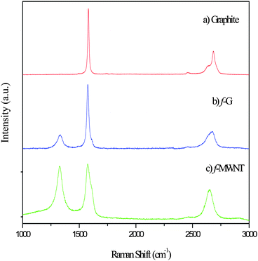
3.2 FT-IR spectroscopy of graphene sheets
Surface modification of MWNT and graphene by functional groups becomes necessary in order to achieve proper dispersion of metal particles. Functionalization was achieved as mentioned earlier and confirmed by FT-IR spectroscopy (Fig. 2). The FT-IR spectra of MWNT and Pt/f-MWNT are reported in our previous work.9 Here, we report the FT-IR spectra of graphene based materials. The peaks corresponding to various functional groups are intense in functionalized graphene (Fig. 2b) while very weak in graphite (Fig. 2a), indicating the presence of a large number of functional groups, thereby validating the functionalization procedure. The broad peak centered around 3430 cm−1 can be attributed to stretching vibrational modes of the hydroxyl group (–OH).17,18 Peaks around 2920 cm−1 and 2850 cm−1 are due to asymmetric and symmetric –CH stretching modes. The peak at ∼1640 cm−1 can be attributed to stretching modes of the –CO group, the peak at 1382 cm−1 is due to the –COO− group and 1060–1015 cm−1 bands corresponds to –CH–OH.19,20 Bulk graphite has some of the above peaks. Clearly, the functionalization procedure has led to the binding of –OH, –COO− and –C![[double bond, length as m-dash]](https://www.rsc.org/images/entities/char_e001.gif) O functional groups on graphene sheets. These are potential sites for the dispersion of metal particles. Hence, there is a reduction in the intensities of these peaks in the case of Pt decorated materials (Fig. 2c).
O functional groups on graphene sheets. These are potential sites for the dispersion of metal particles. Hence, there is a reduction in the intensities of these peaks in the case of Pt decorated materials (Fig. 2c).
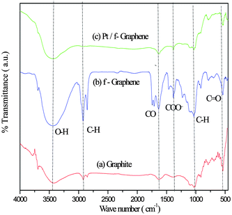 | ||
| Fig. 2 FTIR spectra of (a) graphite, (b) f-G and (c) Pt/f-G. | ||
3.3 Crystallinity of the nanocomposites
Powder X-ray diffractograms (Fig. 3) of the samples have been analyzed to confirm the presence of the deposited elements and the absence of impurities. Fig. 3(a) and 3(b) show the XRD patterns of f-MWNT and f-G. They have been indexed to the peaks of hexagonal graphite. Interestingly, the C (101) peak is prominent in MWNT whereas the C (004) peak is prominent in graphene. Fig. 3(c) and 3(d) are the XRD patterns for Pt/f-MWNT and Pt/f-G, respectively. The fingerprint peaks of platinum are clearly seen along with those of carbon. The broad peak Pt (111) clearly indicates the nanostructured nature of the particles.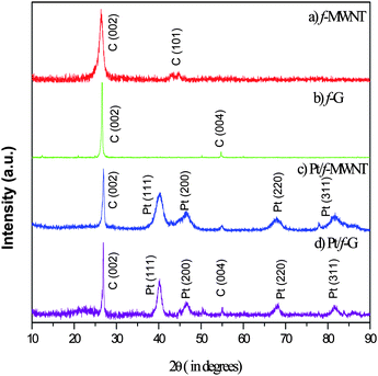
3.4 Morphological analysis of the materials
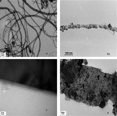
Fig. 4 gives the FESEM images of the sample prepared. Densely packed f-MWNT (Fig. 4a) and Pt dispersed f-MWNT (Fig. 4b) are clearly seen with Pt particles dispersed on the f-MWNT. In Fig. 4(c) flakes of layered graphene sheets are visible and Fig. 4(d) shows the even distribution of Pt particles on the surface of f-G. The dispersion is much better in this case as f-G offers a larger number of active sites where Pt particles can bind.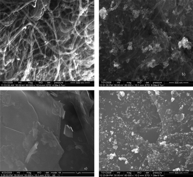
TEM images of the materials are shown in Fig. 5. MWNT with different outer and inner diameters are seen in Fig. 5(a). Fig. 5(b) shows a uniform decoration of a single MWNT by Ptnanoparticles. The layered structure of graphene sheets is clearly seen from Fig. 5(c). A large distribution of Pt particles is clearly visible from Fig. 5(d). Graphene sheets offer an extremely large surface area for Pt dispersion. In some cases the Pt particles also tend to aggregate. The TEM image of graphene sheets presents us with some interesting features concerning the morphology of the graphene sheets. It is the viewpoint of the authors that these layered graphene sheets tend to agglomerate just like the CNTs. By exfoliation of graphitic oxide one may be able to extract very few layered graphene sheets. However, these few layered structures or ‘bunches of few layered graphene’ tend to stack over one another in a way that does not exactly conform to the stacking sequence in graphite (schematic as shown in Fig. 6). This may be termed as the ‘bunch stacking’ morphology. Therefore, in the centre of a stack one may find more graphitic nature as compared to the edges where graphene nature will be predominant. This may also explain the reason why Raman spectra vary from spot to spot on graphene sheets, which is a well known fact.
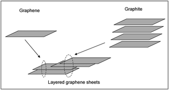 | ||
| Fig. 6 Schematic of the morphology of layered graphene sheets. | ||
3.5 Hydrogen sensing response
Room temperature hydrogen sensing behavior of the sensors S1 and S2 was recorded for a hydrogen concentration of 4 vol% in air. Fig. 7 clearly shows the variation in the resistance of the films as hydrogen gas is periodically allowed and stopped. Two important parameters to be considered while evaluating the performance of these sensors would be their ‘sensitivity’ and their ‘response time’. The sensitivity of a gas sensor is generally defined aswhere Rg = resistance of the film in presence of the gas, Ra = resistance of the film in air. The response time (Tr) of these sensors could be defined as the time taken for its resistance to change from the onset of the change to 90% of its highest value.
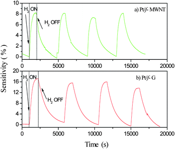 | ||
| Fig. 7 Room temperature hydrogen (4 vol% in air) sensitivity of the sensors: (a) S2 – Pt/f-MWNT and (b) S1 – Pt/f-G. | ||
The sensing performance of the spin coated Pt/f-MWNT (S2) sensor has already been reported by our group elsewhere.9 In close conformity with the reported test results, the drop cast S2 sensor shows a sensitivity of ∼8% and a response time of ∼7 min (Fig. 7a). This justifies the use of the drop casting technique for sensor fabrication. A slightly higher sensitivity is probably due to different types of MWNT used which have been prepared using a different catalyst in the CVD process. The variation in the sensitivity of sensors based on MWNT prepared by different catalysts, though worth investigating is beyond the scope of the present work. The sensor based on Pt/f-G (S1) shows a much higher sensitivity of ∼16% (Fig. 7b), twice that of sensor S2. It shows a response time of ∼9 min. Although, the response times are similar in both the cases, it is clear that the time taken for completing one cycle of hydrogenation and dehydrogenation varies drastically. Graphene based samples take a longer time to regain their original resistance, once the flow of hydrogen is stopped.
The large sensitivity of sensor S1 can be attributed to the fact that graphene offers a larger surface area for platinum dispersion and therefore there are a greater number of active sites for sensing hydrogen. To confirm this, we made films of graphene and MWNT and tested their sensing response. These films showed no response to hydrogen at room temperature even after several cycles of activation. Thus, the difference in the sensitivities can be attributed only to the number of active sites containing Pt. Additionally, the electrical conductivity, mobility and charge carrier density of the underlying carbon nanostructure may also play an important role in the sensitivity.
The accepted mechanism of sensing for the S2 sensor is that in the presence of hydrogen, the work function of Pt is lowered. This causes a transfer of electrons from Pt to the MWNT surface thereby reducing the hole carriers in p-type MWNT. This leads to an increase in the resistance of the material. A similar mechanism must be applicable to graphene sheets. Graphene is a semi metal, theoretically. However, the temperature variation of the resistance of a thin film of graphene sheets shows that it is semiconducting in nature (Fig. 8). Hall effect studies will have to be performed to determine the exact charge carrier type. From the experimental results one could possibly surmise that graphene contains more hole carriers than MWNT. This would result in increased recombination with the electrons coming from Pt, thereby increasing the resistance of the film.
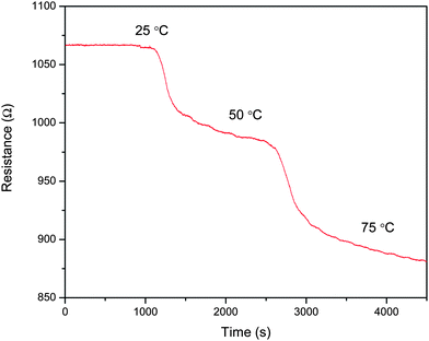 | ||
| Fig. 8 Variation of resistance of temperature of f-G. | ||
The response times of these sensors are comparable. However, their desorption times are different. It appears from Fig. 7 that sensor S2 desorbs faster than S1. Since pure MWNT and graphene films do not show any response to hydrogen, desorption can be attributed to the presence of Pt and not just to the different carbon nanostructures used. Ptnanoparticles on the surface of MWNT or graphene sheets absorb hydrogen and form PtH2. Two competing mechanisms are involved in this process: physisorption and chemisorption. In physisorption, hydrogen molecules stay on the surface of Pt as molecules or as atoms but are bound only by weak van der Waals forces. In chemisorption, the hydrogen atoms enter the lattice of Pt and form the hydride which involves stronger covalent bonds. Hence, it should be more difficult to remove the chemisorbed hydrogen from the Pt lattice than the physisorbed hydrogen. Possibly, graphene allows the Pt particles to chemisorb hydrogen more than MWNT wherein physisorption is preferred. Hence, desorption is faster in Pt/f-MWNT than in Pt/f-G.
4. Conclusion
We report for the first time, the fabrication of a high sensitive room temperature hydrogen gas sensor based on Pt decorated graphene sheets with twice the sensitivity of Pt decorated MWNT. They have similar response times but differ greatly in their desorption times. These sensors fabricated by a simple drop casting technique give sensitivities similar to the reported sensors based on spin coating, making them excellent materials for large scale applications.5. Acknowledgements
The authors are grateful to DRDO, DST and IITM for supporting this work.References
- I. Sayago, E. Terrado, E. Lafuente, M. C. Horrillo, W. K. Maser, A. M. Benito, R. Navarro, E. P. Urriolabeitia, M. T. Martinez and J. Gutierrez, Synth. Met., 2005, 148, 15 CrossRef CAS.
- M. Krishna Kumar and S. Ramaprabhu, Int. J. Hydrogen Energy, 2007, 32, 2518 CrossRef.
- Min Wang and Ying Feng, Sens. Actuators, B, 2007, 123(1), 101 CrossRef.
- Stephanie A. Hooker, Nanotechnology Advantages Applied to Gas Sensor development, The Nanoparticles, 2002 Search PubMed , Conference Proceedings.
- S. Iijima, Nature, 1991, 354, 56 CrossRef CAS.
- M. I. Katsnelson, Mater. Today, 2007, 10, 20 CrossRef CAS.
- P. M. Ajayan, Chem. Rev., 1999, 99, 1787 CrossRef CAS.
- K. S. Novoselov, A. K. Geim, S. V. Morozov, D. Jiang, Y. Zhang, S. V. Dubonos, I. V. Grigorieva and A. A. Firsov, Science, 2004, 306(5696), 666 CrossRef CAS.
- M. Krishna Kumar and S. Ramaprabhu, J. Phys. Chem. B, 2006, 110, 11291 CrossRef.
- M. M. Shaijumon and S. Ramaprabhu, Chem. Phys. Lett., 2003, 374(5–6), 513 CrossRef CAS.
- H. C. Schniepp, J. L. Li, M. J. McAllister, H. Sai, M. Herrera-Alonso, D. H. Adamso, R. K. Prud'homme, R. Car, D. A. Saville and I. A. Aksay, J. Phys. Chem. B, 2006, 110, 8535 CrossRef CAS.
- M. M. Shaijumon and S. Ramaprabhu, Appl. Phys. Lett., 2006, 88, 253105 CrossRef.
- C. A. Ferrari, Solid State Commun., 2007, 143, 47 CrossRef CAS.
- K. N. Kudin, B. Ozbas and H. C. Schniepp, Nano Lett., 2008, 8(1), 36 CrossRef CAS.
- C. Casiraghi, S. Pisana, K. S. Novoselov, A. K. Geim and A. C. Ferrari, Appl. Phys. Lett., 2007, 91, 233108 CrossRef.
- K. S. Subrahmanyam, S. R. C Vivekchand, A. Govindaraj and C. N. R. Rao, J. Mater. Chem., 2008, 18, 1517 RSC.
- W. Qian, T. Liu, F. Wei, Z. Wang, G. Luo and H. Yu, Carbon, 2003, 41, 2613 CrossRef CAS.
- N. I. Kovtyukhova, T. E. Malouk, L. Pan, E. C. Dickey and J. Am, J. Am. Chem. Soc., 2003, 125, 9761 CrossRef CAS.
- N. B. Colthup, L. H. Daly and S. E. Wiberlay, Introduction to infrared and Raman spectroscopy, Boston, Acadamic Press, 1990 Search PubMed.
- U. J. Kim, C. A. Furtado, X. Liu, G. Chen, P. C. Eklund and J. Am, J. Am. Chem. Soc., 2005, 127, 15437 CrossRef CAS.
| This journal is © The Royal Society of Chemistry 2009 |