A facile “liquid-molding” method to fabricate PDMS microdevices with 3-dimensional channel topography†
Xin
Liu
a,
Qi
Wang
*b,
Jianhua
Qin
*a and
Bingcheng
Lin
*a
aDalian Institute of Chemical Physics, Graduate School of the Chinese Academy of Sciences, Dalian, P. R. China. E-mail: bclin@dicp.ac.cn; Fax: +86 411-84379065; Tel: +86 411-84379065
bThe Second Hospital Affiliated to Dalian Medical University, Dalian, P. R. China. E-mail: wqdmu@yahoo.com.cn
First published on 16th February 2009
Abstract
This work deals with a facile “liquid-molding” technology to fabricate PDMS microdevices with complex structured microchannels, the main procedures of which involves: (1) Photo-lithographically fabricating chemical micropatterns of hydrogels on silanized glass substrates to form heterogeneous hydrophilic/hydrophobic surfaces; (2) Fabricating stable 3D surface relief patterns of a liquid viadip-coating the hydrogel patterned substrate in a polar solution; (3) Fabricating PDMS microfluidic devices via a slightly modified replica molding procedure, using a liquid patterned substrate as the molding template. In addition to its simplicity compared to conventional microfabrication methods, this technology produces microchannels with 3D surface topography, which allows for more flexibility in device design and applications. We discuss the main features of the liquid-molding method as well as the structural characteristics of liquid-molded microchannels. We demonstrate the potential application of these “liquid-molded” PDMS (LM-PDMS) devices by designing a cell trapping microdevice that is capable of trapping multiple or individual cells through simple operation procedures.
Introduction
The rapid development of microfluidics has largely benefited from the availability of flexible microfabrication technologies and increasing choices of materials in fabricating microfluidic devices with various structural features and functional capabilities. A widely used material in building microfluidic devices is polydimethylsiloxane (PDMS), a transparent elastomer showing a set of interesting properties being attractive to various microfluidic applications. PDMS microdevices are mostly fabricated through soft lithography technology,1,2 which typically consists of three consecutive procedures: (1) fabricating surface relief patterns of a photoresist (SU-8, for instance) on a planar substrate (mold); (2) replicating the relief patterns into a PDMS substrate through casting and curing processes; and, finally, (3) forming enclosed channel networks by bonding the engraved PDMS to a planar substrate. Despite of their simplicity compared to traditional MEMS based technologies, soft lithography methods still maintain considerable technical thresholds to researchers. The main difficulty lies in the requirement of photolithographical fabrication of the photoresist relief patterns, a process still requiring standard lithographic methods and facilities. For this reason, there has been an interest in developing simpler technologies to fabricate the micromolds, for instance, by writing,3 printing,4 shrinking5 or dip-coating6 based methods. However, most of these new technologies were limited in their capability of producing microchannels with complex structures and functions.On the other hand, there have been increasing interests in the design of microfluidic devices with complex structural and functional features to cope with the rising demand on more advanced applications and operations, for instance, the requirement of microchannels with 3D topographical features to realize fluid pumping,7,8cell9,10 or particle trapping,11,12 or optical sensing functions. To achieve these structural features in microfluidics is even challenging to well-developed standard microlithography technologies. It seems unavoidable to use more advanced technologies, such as multilevel lithography, multilayer alignment or gray-scale lithography, which poses substantial technical and economical thresholds in device fabrication.
We herein propose a simple technology to fabricate PDMS microdevices with complex channel structures. We used a simple and flexible photolithographical technique to pattern chemical coatings of hydrogels on hydrophobic surfaces to form substrates with heterogeneous wetting/de-wetting regions; then formed patterned liquid reliefs on the wetting region through a simple dip-coating procedure; and finally used these “liquid molds” to fabricate PDMS microdevices following a slightly modified replica-molding technique. We termed our technology as a “liquid-molding” (LM) method and the thus fabricated devices as “liquid-molded” PDMS (LM-PDMS) microfluidic devices.
In this work, we discussed the characteristics of the LM method and LM microchannels. We also demonstrated the potential practical application of our technology by fabricating a cell trapping device that was capable of trapping multiple or individual cells.
Experimental
Reagents and instruments
All others reagents were analytical-grade and purchased from various sources. Solutions were prepared in deionized (DI) water.
Experimental methods
The photopatterning assembly was formed by facing a silanized glass slide (upper piece) with a polyester membrane (lower piece). The two pieces were separated at both ends by Teflon spacers (∼100 µm thick) to define out the reaction chamber. Hydrogel precursor was pipetted into the chamber to form a thin layer of solution with the thickness defined by the thickness of the spacers. A transparency mask was then covered on the upper piece to form the completed patterning assembly. Gel patterns were fabricated by exposing the assembly for 4∼10 s under the co-lumniation UV source, at a distance of 30 cm. Immediately after exposure, the patterned glass substrates were successively rinsed with acetone and DI water to remove the un-reacted monomers and photoinitiator.
A fluorescent imaging method was used to qualitatively characterize the topographic features of enclosed microchannels. Briefly, a solution of fluorescein sodium salt was infused into the microchannels and imaged under a fluorescent microscope; based on the correlation of light path length and fluorescent intensity, the topography of the microchannels can be visualized by mapping the fluorescent intensity of the fluorescent images. (see ESI†)
Prior to cell trapping, the microchannels were rinsed with 75% ethanol solution and incubated for several minutes with BSA solution, then filled with PBS buffer. After evacuating all reservoirs, a cell suspension solution was dripped to the entrance reservoir of the main channel. The establishment of hydrodynamic flow facilitated the drifting of the cells into the main channel and being trapped at the trapping region. When a certain amount of cells were trapped, the main channel was flushed with PBS buffer, keeping all other reservoirs empty. Fluorescent reagent solution could be filled in the same way in cell staining experiments.
Results and discussion
Principles and procedures of the liquid molding method
Fig. 1(A) schematically shows the overall work-flow of the liquid molding method, which consisted of a three-step procedure: (1) Photo-lithographically fabricating chemical micropatterns of hydrogels on silanized glass substrates to form heterogeneous hydrophilic/hydrophobic surfaces; (2) Fabricating stable 3D surface relief patterns of a liquid viadip-coating the hydrogel patterned substrate in a polar solution; (3) Fabricating PDMS microfluidic devices via a slightly modified replica molding procedure, by using liquid patterned substrate as the molding template. Fig. 1(B) shows typical examples of the liquid molds and LM microchannels.![Liquid-molding method to fabricate PDMS microdevices. (A) Schematics of the technical procedures. (B) Typical liquid molds [B (a, c)] and LM microchannels [B (b, d)]. (Dye solutions were infused into microchannels to show their workability. Scale bar = 1000 μm.)](/image/article/2009/LC/b818721e/b818721e-f1.gif) | ||
| Fig. 1 Liquid-molding method to fabricate PDMS microdevices. (A) Schematics of the technical procedures. (B) Typical liquid molds [B (a, c)] and LM microchannels [B (b, d)]. (Dye solutions were infused into microchannels to show their workability. Scale bar = 1000 μm.) | ||
Self-organization of liquids on surfaces with patterned wetting/de-wetting properties is a well known phenomena and has been of recent interest in developing new microfabrication technologies to producing micro-objects with complex shapes.13–15 The formation of patterned liquid reliefs on planar surfaces is typically achieved by, first, patterning a chemically homogeneous surface with chemical coatings of opposite wetting/de-wetting properties, through photo or soft lithographical procedures;14 Liquid structures seated on either wetting or de-wetting regions are then formed by condensation or dip-coating procedures.
In this work, we developed a simple technique to produce stable liquid (glycerol) relief patterns on 3-(trimethoxysiyl) propyl methacrylate (TPM) silanized surfaces. We first pattern the initially hydrophobic TPM surfaces with regions of hydrophilic polyacrylamide (PAAM) hydrogels,16 by sandwiching a thin layer of monomer solutions containing a photoinitiator and on-set UV illumination through a transparency photomask, forming stable patterned coatings of pAAM that covalently bonded with the methacrylate group on the silane reagent which, in turn, bonded on the substrate surface (see ESI†). We then submerge the gel patterned TPM substrate into a bath of glycerol and vertically pull the substrate out of the liquid. Being a polar reagent, glycerol tends to wet the gel patterns and de-wet the TPM surface, thus, during the aforementioned dip-coating process, the inter-play of capillary force and shear stress resulted in forming glycerol droplets or stripes seating on gel patterns and pinned along the border between hydrogel (wetting) and TPM (de-wetting) regions (see Movie S1, ESI†).
By using this technique, we fabricated glycerol relief patterns with desired channel structures by simply designing and using appropriate negative photomasks to fabricate the hydrogel micropatterns. The feasibility of using these glycerol patterns as the molding substrate to fabricate PDMS microchannels relied on the factors that (1) the PDMS precursor is a nonpolar liquid, which is immiscible with glycerol, (2) at micrometer scale the relative large capillary force over-rides the influence of gravity and shear force on the stability of liquid structures, (3) glycerol is a liquid with low vapor pressure (0.4 k Pa at 20 °C) and high boiling point (182 °C), its micropatterns will be stable at the curing temperature (60–80 °C) of PDMS. We thus may use these glycerol micropatterns as the replica template to fabricate PDMS microdevices, following procedures used in soft lithography. The only precaution needed was to gently pour PDMS precursor over the liquid mold to minimise the shearing force on the glycerol patterns.
The minimum channel width obtainable by the LM method was limited by the resolution of hydrogel patterning. Due to un-avoidable diffusion and diffraction effects during UV exposure, the minimum pattern width of the hydrogel was ∼60 μm, which was also the lower limit of the channel width of the LM-PDMS microdevices.
Since the fidelity in channel width with respect to mask design was determined by fidelity in producing hydrogel micropatterns, the optimization on solution composition and exposure dosage16 was necessary to produce microchannels with desired dimensions (see Fig. S2, ESI†)
Characteristics of the liquid molding method
One apparent feature of the LM method was its simplicity compared to standard soft lithography method. The two methods differed in the technique in producing micromolds. As compared in Fig. 2, instead of fabricating photoresist micromolds by going through standard photolithographical steps and using specialized facilities, LM method relied on a facile photopatterning procedure to fabricate hydrogel micropatterns, followed by very simple dip-coating operations, thus greatly simplified the overall processes of device fabrication. | ||
| Fig. 2 Comparisons between the liquid molding method and conventional methods. | ||
Chao et al. proposed a rapid fabrication method to produce microchannels by using microscale plasma activated templating generated water molds.6 Their work relied on patterned hydrophilizing PDMS substrates with oxygen plasma by using stencil masks, then using the thus treated substrates to produce liquid molds. This method was limited in pattern fidelity and geometry due to the mechanism of plasm oxidation and the difficulties in producing the stencil masks. Besides, the stability of the wetting/de-wetting patterns on PDMS substrates is questionable, since PDMS tends to quickly recover to its initial physical properties after chemical or physical treatments. In contrast, we fabricated wetting/de-wetting patterns by photopatterning a pAAM hydrogel that was stably bonded on the TPM surfaces. Moreover, being free to design and produce mask patterns with various geometrical features, our method showed superior flexibility in producing liquid molds with more complex structures.
Another interesting feature of LM method was that it produce micromolds, henceforth, microchannels with more complex surface topographies, in comparison to those fabricated through planar lithography. As also compared in Fig. 2, instead of producing step or column shaped micro-objects, LM methods produced micro-objects with curved surfaces, and the surface topography were determined by the 2D geometries prescribed in the photomasks. The important implication of this feature is that, by changing the size or geometries of mask patterns, we may easily tune the 3D structures of the microchannels, as discussed in next section.
Characterization of liquid molded microchannels
In contrast to planar lithography, the LM method is essentially a 3D microfabrication technology that produces topographically 3D structures from 2D geometries prescribed in the photomask. The 3D surface geometry of the liquid droplets seating on patterned wetting/de-wetting substrates was correlated to the size and geometry of the 2D wetting base, henceforth the size and geometry of the mask patterns.A most straightforward application of this feature was to produce microchannels with different heights by simply controlling the width of the line patterns in the photomasks. As shown in Fig. 3, we prepared a series of straight LM channels of widths ranging from 50∼500 μm (Fig. 3A) and measured their cross-sectional profile with a surface profilometer (Fig. 3B). As was predictable, LM channels had a curved cross-sectional profile. Moreover, we observed a linear relationship between the apex height and base width of the microchannels (Fig. 3C), and the ratio of the two (aspect ratio) was determined to be 0.1.
 | ||
| Fig. 3 Structure measurement of liquid molded microchannels. (A) Micrograph of liquid strips of various width. (B) Cross-sectional profile of molded microchannels. Insert is a micrograph showing the cross-section of an enclosed microchannel. (C) Correlation of channel widths and apex heights. (Scale Bar = 500 μm.) | ||
The fixed low aspect ratio of LM microchannels might limit the flexibility of the LM method, however, as it is known that the apparent contact angle of the liquid on patterned substrates can be tuned by changing the volumes of the droplets,14 one might possibly increase the aspect ratio of the LM microchannels, say, by further increasing the volumes of the dip-coated liquid patterns via vapor phase condensation. Moreover, as exemplified in the following cell trapping applications, the fixed low aspect ratio can also be a beneficiary factor in device design.
Being free to fabricate gel patterns of various geometries, we may produce LM channels with even more complex structural features, as shown in Fig. 4. To characterize these complex-structured microchannels, we developed a facile fluorescent imaging technique to directly visualize their 3D topography and analyze their local structural features. As shown in Fig. 4(b), we infused a fluorescent dye into LM microchannels and took fluorescent images under fluorescent microscope; we then used image analysis software to directly map the fluorescent intensity into topographical figures (Fig. 4(c)). According to the positive correlation between fluorescence intensity and light path length, the intensity of topographic figures shown in Fig. 4(c) could also be taken as qualitative presentations of the geometric topography of the microchannels (see ESI†). Based on the same principle, we may also characterize cross-sectional profiles of the channels by measuring fluorescence intensity along specific lines in the fluorescent images (Fig. 4(d)).
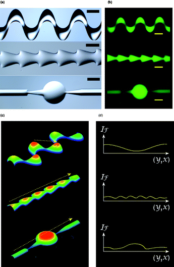 | ||
| Fig. 4 Characterization of the complex structured microchannels via a fluorescent imaging technique. (a) Liquid molds with complex structures. (b) Fluorescent images of LM microchannels molded from the liquid molds shown in (a). (c) Intensity mapping of the fluorescent images revealing the 3D structures of the microchannels. (d) Cross-sectional profiles alone the lines showing in (c) (Scale bar = 1000 μm.) | ||
Liquid-molded cell trapping devices
As shown in Fig. 3 and 4, the LM method allows for fabrication of microchannels with variant local 3D topography, this feature will allow for more flexibilities in device design and applications. We herein shown an example of practical applications of this feature by design a LM microdevice capable of trapping and manipulating multiple or individual cells.Cell trapping is a highly demanding functionality in physical or chemical cell manipulations or real-time physiological process observations. To realize cell trapping in microfluidic devices, the typical strategy used was to fabricate, for instance, dam,10 bowl,9 or sieve17 structures that physically dock cells at a desired location within a microfluidic network. The challenges in fabricating these devices lies in (1) the requirement of fabricating fine structures of sizes down to the cellular scale (several micrometers, for instance), which require high-resolution lithography techniques and facilities, and (2), in some cases, the demand of multi-level fabrication technologies to fabricate microchannels with varying heights. We herein show the use of LM technology to fabricate a simple structured cell trapping microdevice capable of trapping and staining multiple or individual cells.
Fig. 5(A) shows the design and the structural features of our LM cell trapping device. We used the LM method to produce T-shaped channel networks, with a portion of constriction of the microchannel at the intersection of the main channel and accessary channels (trapping region). The width of the main channel and accessary channel were designed to be 500 μm and, at the trapping region, the channel width narrowed down to 60∼100 μm (Fig. 5(A(b))). As shown in Fig. 5(A(c)), the narrowing of the trapping channel resulted in a substantial reduction in apex channel height. Taking Fig. 3(C) as a reference, we estimated that the narrowing of the channel width to 60∼100 μm correspond to apex channel height of < 10 μm, a size range comparable to the size of mammalian cells. Thus, the cells flowing towards the accessary channel will be blocked by the trapping channel (Fig. 5(B))). In cell trapping experiments, we infused a buffer solution into the channel network, then evacuated all the channel wells, and dripped a cell suspension into the inlet of the main channel. The on-set of hydrodynamic flow facilitated the drifting of the cells into the main channel, and the hydrostatic pressure drop across the main channel and accessary channels drew the cells to flow towards the trapping region and became trapped at the upper end of the trapping channel. Fig. 5 (C) shows time-sequential images of the trapping process (see Movie S2, ESI†).
 | ||
| Fig. 5 Cell trapping devices fabricated from the LM method. (A) design and characterization of cell trapping device; (a, b) Device design; (c) Structural characterization via fluorescent imaging. (B) Working principle of cell trapping devices. (C) Sequential images showing the trapping process. (Time interval = 15 s, scale bar = 200 μm.) | ||
Further treatment of the trapped cells, for instance, cell staining, was also feasible. Keeping the outlet reservoirs vacant, we flushed out un-trapped cells in the main channel by dripping a buffer solution into the inlet reservoir of the main channel, leaving the trapped cells maintained at the trapping region by the persistent hydrostatic pressure. Using the same procedure, we infused a dye solution into the channel network and stained the cells fluorescent (Fig. 6A).
 | ||
| Fig. 6 Chemical manipulation of trapped cells. (A) Sequential images showing the process of fluorescent staining of trapped cells. (Time interval = 2 s.) (B) live/dead assay of trapped cells. (C) Trapping and staining single cell; (a) fluorescent image showing the trapped single cell; (b) Sequential images showing AO/EB staining of the single cell (time interval = 3 s); (c) Temporal change of fluorescent intensity on the cell. (Scale bar = 200 μm.) | ||
Fig. 6B shows the result of live/dead staining of the trapped cells. The green fluorescence of most cells indicated that the trapping process was gentle enough to keep the viability of the cells.
It was also feasible to control the number of trapped cells by, for instance, tuning the width of the trapping channel (results not shown) or adjust the concentration of cell suspension. For instance, by infusing a low-concentration cell suspension into the main channel, we may, by chance, trap a single cell at the trapping region. Fig. 6(C) shows a single cell trapped at the trapping region (Fig. 6(C(a))), and the process of stain of the cell with acridine orange (AO)/ethidiumbromide (EB) (Fig. 6 (C (b)), Movie S3, ESI†), which shows a potential application of our cell trapping device in real-time monitoring of cellular processes.
Conclusion
In this work, we developed a liquid molding method to fabricate microfluidic devices. Our technology was appealing in its simplicity. Besides, being a microfabrication technology principally different from traditional planar lithography, the liquid molding method was capable of producing microchannels with 3D surface topography and allowed for more flexibilities in device design. We showed an example of the potential application of our LM technology by designing and testing a cell trapping microdevice.One may note that there may be some other applications of the LM method, such as, fabricating optical components or diffuser pumps for microfluidic applications.
Acknowledgements
This research was supported by the Natural Science Foundation of China (Grant no. 20635030, 20575067 and 30670532), Hi-Tech Research and Development Program of China (863 Program) (Grant no. 2006AA020201) and Chinese Academy of Sciences Knowledge Innovation Program (Grant No. K2006A11).References
- Y. N. Xia and G. M. Whitesides, Angew. Chem., Int. Ed., 1998, 37, 551–575 CrossRef CAS.
- D. C. Duffy, J. C. McDonald, O. J. A. Schueller and G. M. Whitesides, Anal. Chem., 1998, 70, 4974–4984 CrossRef CAS.
- D. Therriault, S. R. White and J. A. Lewis, Nat. Mater., 2003, 2, 265–271 CrossRef CAS.
- J. C. McDonald, M. L. Chabinyc, S. J. Metallo, J. R. Anderson, A. D. Stroock and G. M. Whitesides, Anal. Chem., 2002, 74, 1537–1545 CrossRef CAS.
- A. Grimes, D. N. Breslauer, M. Long, J. Pegan, L. P. Lee and M. Khine, Lab Chip, 2008, 8, 170–172 RSC.
- S. H. Chao, R. Carlson and D. R. Meldrum, Lab Chip, 2007, 7, 641–643 RSC.
- C. Yamahata, C. Vandevyver, F. Lacharme, P. Izewska, H. Vogel, R. Freitag and M. A. M. Gijs, Lab Chip, 2005, 5, 1083–1088 RSC.
- M. A. Unger, H. P. Chou, T. Thorsen, A. Scherer and S. R. Quake, Science, 2000, 288, 113–116 CrossRef CAS.
- D. Di Carlo, N. Aghdam and L. P. Lee, Anal. Chem., 2006, 78, 4925–4930 CrossRef.
- M. S. Yang, C. W. Li and J. Yang, Anal. Chem., 2002, 74, 3991–4001 CrossRef CAS.
- L. Ceriotti, N. F. de Rooij and E. Verpoorte, Anal. Chem., 2002, 74, 639–647 CrossRef CAS.
- D. S. Peterson, Lab Chip, 2005, 5, 132–139 RSC.
- H. A. Biebuyck and G. M. Whitesides, Langmuir, 1994, 10, 2790–2793 CrossRef CAS.
- P. Lenz, Ad. Mater., 1999, 11, 1531 Search PubMed.
- Y. N. Xia, D. Qin and Y. D. Yin, Curr. Opin. Colloid Interface Sci., 2001, 6, 54–64 CrossRef CAS.
- V. A. Liu and S. N. Bhatia, Biomed. Microdevices, 2002, 4, 257–266 CrossRef CAS.
- A. Valero, F. Merino, F. Wolbers, R. Luttge, I. Vermes, H. Andersson and A. van den Berg, Lab Chip, 2005, 5, 49–55 RSC.
Footnote |
| † Electronic supplementary information (ESI) available: Fig. S1–4 and Movies S1–3. See DOI: 10.1039/b818721e |
| This journal is © The Royal Society of Chemistry 2009 |