Combinatorial atmospheric pressure chemical vapour deposition (cAPCVD) of a mixed vanadium oxide and vanadium oxynitride thin film
Andreas
Kafizas
,
Geoffrey
Hyett
and
Ivan P.
Parkin
*
Materials Chemistry Research Centre, Department of Chemistry, University College London, 20 Gordon Street, London, UK WC1H 0AJ. E-mail: i.p.parkin@ucl.ac.uk
First published on 28th January 2009
Abstract
A novel combinatorial atmospheric pressure chemical vapour deposition (cAPCVD) technique was used to synthesise numerous vanadium oxide and vanadium oxynitride phases on a single film. This is the first example of cAPCVD having been used to synthesise a gradating mixed anion system. The film was characterised by X-ray diffraction (XRD) mapping, Raman, wavelength dispersive X-ray analysis (WDX) and X-ray photoelectron spectroscopy (XPS) analysis of positions along the film's front edge allowed the chemical composition to be determined and correlated with XRD data. Film thicknesses were determined using side-on scanning electron microscopy (SEM). Functional property mapping of the optical transmittance/reflectance and electrical resistance allowed systematic investigation on the effects of oxygen content within a vanadium oxynitride film. cAPCVD used in conjunction with mapping analysis tools is a shortcut for identifying numerous, phases, compositions and properties and their relationships on a single film, and offers a rapid method for analysis of phase-space.
Introduction
Combinatorial atmospheric pressure chemical vapour deposition (cAPCVD) is a relatively new synthetic technique that has been used to create a variety of mixed phase and composition thin-film systems on a single substrate.1–3 A given cAPCVD system can show many different phases and properties across a film and has been used to optimise functional properties and discover new materials.2,3Atmospheric pressure chemical vapour deposition (APCVD) has been used to synthesise vanadium nitride4–6 and a variety of vanadium oxides.7–15 Interest has been shown in vanadium nitride for its solar control properties, where thinner coatings (≈ 150–250 nm thick) can show a combination of transmission and reflection properties that enable the passage of visible light through the coating but are highly reflective at infrared wavelengths.4–6 Thicker coatings have been shown to transmit far less visible light yet show stronger infrared reflectivity.16 A recent study of titanium nitride films of differing thicknesses displayed significant deviations in the optical transmittance/reflectance with film thickness.17
Vanadium nitride films formed via the APCVD route inadvertently incorporate oxygen, with some films classified as nitrides having oxygen content as high as 30 atom%.4 It is well known that oxygen contamination can alter the hardness, conductivity, and infrared reflectivity properties of vanadium nitride coatings.6 It is not known, however, by how much each property will deviate upon oxygen contamination at a given thickness. In synthesising vanadium oxynitrides via the cAPCVD route, access to a range of differing oxygen contents on a single film is possible.
Although a variety of vanadium oxide phases have been formed viaAPCVD, vanadium dioxide has been the most extensively studied.7–12 At room temperature, VO2 contains a distorted arrangement of V4+–V4+ pairs with localised d-electrons. This monoclinic phase is infrared transparent and semiconducting. Above 68 °C, a phase transition to tetragonal occurs, releasing the d-electrons into the conduction band and giving metallic infrared reflectivity. There is considerable interest in the application and optimisation of this property, termed ‘thermochromism’ for use in window coatings.7–12
In this paper, we describe the combinatorial atmospheric pressure chemical vapour deposition (cAPCVD) synthesis of a film with gradating phases from triclinic V8O15, to hexagonal V2O3, to a range of cubic VOxN1−x (0.23(4) ≤ x ≤ 0.53(4)) using a triple source of precursors: VCl4 [metal source], H2O [oxygen source], and NH3 [nitrogen source]. This is the first time cAPCVD has been used to synthesise a gradating mixed anion system. The varying phases were characterised by powder X-ray diffraction (XRD), and mapping specific points across and along the film. The Rietveld method was used to refine a phase model against the collected XRD data. Vegard's law,18 used in conjunction with a phase model, allowed for the prediction of percentage nitrogen content at each oxynitride position analysed. Raman, wavelength dispersive X-ray (WDX) and X-ray photoelectron spectroscopy (XPS) analysis of analogous positions along the film's front edge allowed for correlations against XRD analysis to be made. The thickness at each point was determined using side-on scanning electron microscopy (SEM). A relationship between oxygen incorporation within vanadium nitride and the conductivity and optical reflectance was made. Therefore, a direct indication of the effect of oxygen contamination upon the solar control properties of vanadium oxynitrides was concluded.
This application of cAPCVD demonstrated the ability of a non-conventional technique to produce numerous phases and compositions within a single film. The possibilities for determining relationships for functional property optimisation of mixed ion systems, in conjunction with map analysis techniques, are extensive. This method offers the possibility to rapidly explore phase space, especially as the analysis can be achieved by semi-automated means.
Experimental
Film synthesis
Thin films were synthesised by cAPCVD using a cold-walled reactor with the sample being deposited onto standard float glass slides of dimensions 89 × 225 × 3.2 mm (horizontal, lateral, thickness). The glass slides were coated on the top surface with a barrier layer of SiO2 (50 nm thick) to prevent ions in the glass from migrating into the synthesised film. The substrates were washed with acetone and isopropanol, and air-dried prior to use. The apparatus used is shown schematically in Fig. 1. | ||
| Fig. 1 Schematic diagram of the cAPCVD apparatus, with top-down view of the reactor. Of particular importance are the three separate entry points to the reactor, mixing chamber A (on the right), mixing chamber B (in the middle) and the ammonia line (on the left). Left, middle and right in this context are orientated with the forward direction being through the reactor toward the exhaust. | ||
VCl4 (Aldrich 99.9%) [Bubbler 2] and H2O [Bubbler 1] were volatized in heated bubblers. The reagents were transported to their respective mixing chambers [A = H2O, B = VCl4] by N2 (BOC, oxygen free) carrier gas and combined with a plain line of N2. The reagents were then passed through the triple entry baffle manifold that inhibited mixing until the gas flows were inside the reactor with H2O through the right, VCl4 through the middle and NH3 (BOC, anhydrous) transported under its own vapour pressure through the left. This produced the conditions for the combinatorial aspect of this work, as the oxygen and nitrogen sources entered from opposite sides of the reactor, creating a gradient in the O : N ratio present in the precursor mix horizontally across the substrate and thus a range of deposition conditions in a single experiment.
The use of three precursors provided us with a large number of experimental parameters; therefore, for simplicity the bubbler, reactor and mixing chamber temperatures were kept constant and only the plain flow and precursor flow rates were varied with each experiment. This was undertaken until a single film with significantly visible horizontal compositional variation was achieved (thick vanadium nitride films being black mirrors and vanadium oxide films ranging from blue to yellow with greater transmittance). The parameters used to achieve this combinatorial film across a portion of the film are displayed in Table 1.
Analytical methods
The section of the thin film that lay closer to the exhaust was chosen for analytical study due to the greater variation in compositional gradient where an 89 × 112 × 3.2 mm (horizontal, lateral, thickness) piece was cut and labelled (Fig. 2).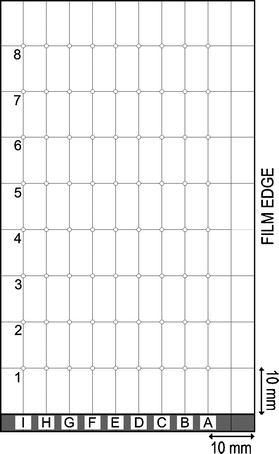 | ||
| Fig. 2 Diagram representing the labelling of all positions analysed, and the specific positions that were analysed by each method of characterisation used. Row 1 is closest to the reactor inlet and row 8 closest to the exhaust. | ||
X-Ray diffraction (XRD) mapping was carried out using a micro-focus Bruker GADDS powder X-ray diffractometer, with a monochromated Cu Kα1 (1.5406 Å) source, and a CCD area X-ray detector, capable of 0.01° resolution in 2θ with an automated X–Y movable stage. Seventy-two points were analysed at the positions specified in Fig. 2, which shows the reference system used throughout the paper. The spectra were acquired in a single overnight experiment by programming the computer-controlled movable X–Y stage. The instrument was used in the glancing incident angle geometry that is best suited to the investigation of films; a θ1 value of 5° was used. The recorded diffraction data were compared with database standards; the peaks identified as cubic vanadium oxynitride were analysed by comparison with a Rietveld19 refined model using the GSAS and EXPGUI software suite.20 The oxygen–nitrogen ratio of every vanadium oxynitride position analysed was predicted with use of Vegard's law and their extracted cubic lattice parameter.
X-Ray photoelectron spectroscopy (XPS) was conducted using an Escalab 220i-XL instrument with Al Kα radiation for 9 positions across the front of the film (Fig. 2). Survey scans were recorded in the range 0–1100 eV (binding energy), and then smaller range, higher resolution scans were recorded of the principal peaks of V (2p), O (1s), N (1s), C (1s) and Si (2p). The peaks were modelled using the CasaXPS software system to determine their area. The peak areas were adjusted using sensitivity factors21 to allow the film composition to be calculated.
Wavelength dispersive X-ray (WDX) analyses using a Philips SEM referenced against silicon, vanadium, nitrogen and oxygen standards over a 1 µm diameter spot size for 9 positions across the front of the film and an additional 8 positions 1.67 mm either side of F1, G1, H1 & I1 (Fig. 2) were performed (this procedure can also be conducted by using an overnight computer-controlled system). The weight percentages of each element analysed was extracted and normalised using the INCA software system,22 thus allowing stoichiometric ratios to be determined.
Raman spectroscopy was performed on a Renishaw 1000 spectrometer using a 632.8 nm laser. The laser power was significantly reduced to prevent laser-induced oxidation,23 calibrated to the emission lines of carbon at 2 mW. 9 positions across the front of the film (A1–I1), manoeuvred using an X–Y stage, were analysed in the range 100–1200 cm−1 (Fig. 2).
UV-visible transmission and reflection spectroscopy was conducted using a Helios double beam instrument, built for compatibility with samples of thin films on glass substrates, for 40 positions (Fig. 3) through a pin-hole (radius 5 mm). Measurements were standardised relative to a rhodium mirror (reflectance) and blank glass slides (transmittance). Transmission and reflection spectra were recorded in the range 300–2500 nm.
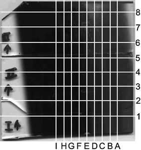 | ||
| Fig. 3 Scanned image of the film chosen for study. From left to right the gradating black to dark navy blue to brown yellow colours are observed indicating the multiple phase transitions across the film. | ||
The electrical resistance was measured using a Digitec CAT.II 600V dual-point multimeter for all 72 positions (Fig. 2) where the anodes were placed 2 mm apart.
The thickness was measured by snapping the film at the respective position, mounting it side-on and SEM imaging the sample using a JOEL-6301F field emission instrument, using secondary electron imaging (Fig. 2).
Results
Physical characterisation
By visual inspection, the film chosen for study covered the glass sheet and contained gradating colour from a black mirror to dark navy blue to a brown yellow from left to right (from columns I to A: Fig. 3). The film was adhesive and impervious to 24 h immersion in common solvents (water, acetone and isopropanol). Side-on SEM imaging studies determined the median growth rate was 3.1 nm s−1 (standard deviation 1.2 nm s−1) at a substrate temperature of 630 °C.Characterisation
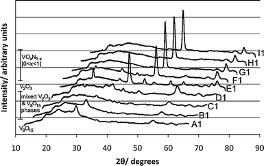 | ||
| Fig. 4 An offset stack plot of the XRD data obtained from the positions analysed from the front row of the combinatorial film chosen for study. The phase transitions from triclinic V8O15 at A1, to hexagonal V2O3 at E1, to cubic vanadium oxynitrides F1–I1 are observed. | ||
| (a) | a/Å | |||
|---|---|---|---|---|
| 8 | 4.1102 | 4.1013 | 4.0950 | n/a |
| 7 | 4.1122 | 4.1073 | 4.0949 | n/a |
| 6 | 4.1123 | 4.1086 | 4.1005 | n/a |
| 5 | 4.1140 | 4.1108 | 4.0999 | 4.0889 |
| 4 | 4.1149 | 4.1113 | 4.1037 | 4.0988 |
| 3 | 4.1150 | 4.1120 | 4.1043 | 4.1044 |
| 2 | 4.1152 | 4.1106 | 4.1067 | 4.1024 |
| 1 | 4.1199 | 4.1150 | 4.1093 | 4.1058 |
| I | H | G | F | |
| (b) | ||||

|
 | ||
| Fig. 5 A comparison of the nitrogen to oxygen molar ratios obtained viaWDX (A1–I1 and 1.67 mm either side of F1–I1) and application of Vegard's law to Rietveld refined XRD data (A1–I1) for positions across the front row, where the correlation convincingly validates the application of Vegard's law. The standard deviation of the numerical difference between the two data sets was taken as the error in the Vegard's law N% calculations. | ||
 | ||
| Fig. 6 All-phase map of the 72 positions XRD analysed. The numbers are indicative of the nitrogen to oxygen percentage of the oxynitride phase estimated with the use of Vegard's law and Rietveld analysis. | ||
Analysis of all the XRD data obtained, enabled a map of the entire substrate to be constructed (Fig. 6). Due to the quality of the XRD data obtained, as well as the problems associated with preferred orientation, it was not possible to give accurate phase proportions within the mixed vanadium oxide section of the film. The positions within this section were consequently grouped after inspection of their respective XRD pattern's shape and a qualitative measure of the phase proportions was attained.
 | ||
| Fig. 7 Peak deconvolution analysis of stacked V 2p spectra revealed three distinct vanadium environments; V5+ (V–O), V3+ (V–O) and V3+ (V–N). The transition from a vanadium oxide to a vanadium oxynitride phase, as well as the increase in nitrogen incorporation from positions A1–I1 is observed. | ||
Peak deconvolution analysis within the N 1s energy range also yielded three separate environments (Fig. 8). From positions A1–E1 two peaks within the ranges 399.6–399.9 eV and 401.5–401.7 eV, related to surface-bound nitrogen29 and oxidised surface-bound nitrogen.30 At position F1, a third environment at 396.5 eV, related to N3− was seen,28 indicating the initiation of the oxynitride phase. Analysis of further oxynitride positions from G1–I1 showed a steady increase in the intensity of the N3− environment. This corresponded to an increase in nitrogen incorporation within the oxynitride phase, and with information derived from the deconvolution of the V2p spectra, in agreement with WDX and XRD analysis.
 | ||
| Fig. 8 Peak deconvolution analysis of stacked N 1s spectra unveiled three separate nitrogen environments; oxidised and un-oxidised surface-bound nitrogen and N3− (V–N). The initiation of the oxynitride phase, as well as the increase in nitrogen incorporation from positions F1–I1 is observed. | ||
Deconvolution of the XPS spectra within the O 1s binding energy range unveiled three distinct environments across the front positions related to V–O V3+ and V5+.27,31 A comparison of the average oxidation state of vanadium derived viaXRD and XPS analysis demonstrated higher surface oxidation environments for all front row positions (Table 3), this difference being common for cAPCVD synthesised films due to the surface oxidation that occurs at the end of a deposition upon cool-down inside the reactor.
 | ||
| Fig. 9 Stacked representation of all front row positions, A1–I1, Raman analysed in the 100–1200 cm−1 range. The transition in symmetry from predominantly monoclinic VO2-like, to hexagonal V2O3 to cubic vanadium oxynitride is observed from analysis of A1–I1. | ||
The similarity in structural symmetry of triclinic V8O15 and monoclinic VO2 allowed for comparisons of Raman patterns of the triclinic phase to be made against the monoclinic phase, a direct triclinic literature example was unavailable due to the narrow study of this Magneli phase. Positions A1–C1 showed symmetry similar to monoclinic VO2, attributable to the triclinic V8O15 phase detected viaXRD. The Raman spectrum of the phase mixed monoclinic and hexagonal symmetry pattern seen at position D1 coincided with the mixed phase pattern observed viaXRD (Fig. 4). Both Raman and XRD indicated the presence of single-phase hexagonal V2O3 and the transition to cubic symmetry from F1 onwards.
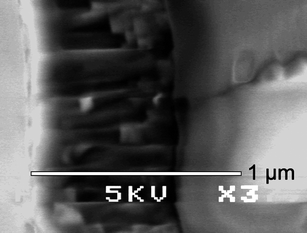 | ||
| Fig. 10 Side-on SEM image of position I1 showing the preferred orientation growth of the crystallites of the vanadium oxynitride phase. | ||
A colour-coded map presentation of the thicknesses demonstrated the deviation of the thickness across the film (Fig. 11). For the deposition, a carbon block was used to heat the substrate. The block's heating is fairly uniform (within ca. 25 °C), however, the hottest point is in its centre where film growth on the overlying substrate occurs most rapidly. The top-half of the film was chosen for analytical study, where central positions in row 1 lie closest to the centre of the block. It is therefore intuitive, for a surface reaction rate limited CVD process that the further the position analysed was from this area, the thinner the film was observed to be.
 | ||
| Fig. 11 Thickness map calculated using side-on SEM images of a snapped edge at each respective position for all 72 points; numbers represent the thickness at that positions in nanometres and the colour key corresponds to the thickness. | ||
Top-down SEM images of all positions along column I were taken. The images showed similar grainy morphologies of the vanadium oxynitride section with crystallite sizes of roughly 100 nm in diameter. An example image of position I1 is shown in Fig. 12.
 | ||
| Fig. 12 An example top-down SEM image of position I1 demonstrating the grainy morphology of this vanadium oxynitride section of the film. | ||
Three distinct phases were observed gradating across the film from triclinic, Magneli V8O15 on the right, to hexagonal, V2O3, to a range of cubic VOxN1−x (0.23 ≤ x ≤ 0.53) on the left. From structural observations it can be seen that V8O15 is merely an oxygen-deficient form of VO2. This vanadium species was found nearest the oxygen source inlet. Further from this inlet mixed V8O15–V2O3 phases of lower average oxidation state were formed and further yet, near the centre of the film, hexagonal V2O3 was solely observed (Fig. 6). Above 600 °C with an excess of water over the vanadium precursor, the formation of VO2 over V2O3 is preferential.11
From the nature of the decrease in oxidation state of vanadium in the vanadium oxides, where the highest oxidation state observed was nearest the oxygen source inlet, it is clear that the formation of the oxygen deficient VO2 species was preferential. A lesser water presence further from its inlet encouraged lower oxidised V2O3 phase formation.
On the left side of the film, due to the higher concentration of the nitrogen source over the oxygen source, vanadium oxynitrides were formed. XRD analysis showed that the % N incorporation was dependant upon the distance from the nitrogen source where the highest % N incorporations were observed nearest the nitrogen source inlet and decreased outwards in a diagonal fashion (Fig. 6). A few positions at the top middle section of the film displayed a mixed V2O3–oxynitride phase; however, due to the localisation of the nitrogen source in comparison to oxygen, the degree of mixed V2O3–oxynitride phases seen in comparison to V8O15–V2O3 phases was far lower.
Functional properties
 | ||
| Fig. 13 A UV-vis transmittance spectrum of positions analysed across row 6 of the vanadium oxide–oxynitride film in the 300–2500 nm range. The transition from a light transmitting to a highly reflective material is intuitively what one would expect given the film's transition from a vanadium oxide to an oxynitride. | ||
A transition from a light-transmitting (positions A6 and C6) to a highly reflective material (G6 and I6) was observed. This is in agreement with the optical properties associated with the characterised phases for each position analysed, as vanadium oxides are generally quite light-transmitting materials whilst vanadium oxynitrides are often black and highly reflective. The reflectivity data is also in agreement with this, whereby the VON positions analysed displayed reflectances of 70% or greater observed at 1500 nm. A close-up of the spectra obtained from analysis of column I is shown below (Fig. 14).
 | ||
| Fig. 14 A UV-vis reflectance spectrum of the positions analysed along column I. High reflectivity was observed for all positions due to the metallic nature of vanadium oxynitrides. | ||
A trend in decreasing reflectance from position I1 outwards was observed. This was attributed to the decrease in the metallic nature of the film as the oxynitride's nitrogen incorporation decreased outwards from position I1 as well as its reflectivity. The decrease in reflectivity was not attributed to film thickness or any morphological differences as a 0% transmittance was observed over the entire 300–2500 nm range and a consistently grainy surface with similar crystallite diameters was seen for all positions along column I (Fig. 12). A relationship between nitrogen incorporation within a cubic vanadium oxynitride film over the range VOxN1−x (0.23 < x < 0.37) and its reflectance at 1500 nm was established (Fig. 15).
 | ||
| Fig. 15 A plot of percentage reflectance at 1500 nm against nitrogen percentage incorporation of the vanadium oxynitride positions analysed in column I. A regression analysis yielded a degree of correlation of 0.952, whereby an outlier at 66% N incorporation was disregarded. | ||
The relationship between nitrogen incorporation and reflectance fit a linear model best, however, the range is quite narrow relative to the number of VOxN1−x [0 < x < 1] phases accessible. Further analysis of a wider VOxN1−x range is required to ascertain whether or not a linear model would collapse near the boundaries [x approaches 1 or 0]. Inclusion of the reflectance data observed in row G would have certainly expanded the range; however, the use of the narrowest slit on the spectrophotometer allowed slight (less than 10%) overlap of the neighbouring oxides in column F. The resulting data was then somewhat skewed toward lower reflectance.
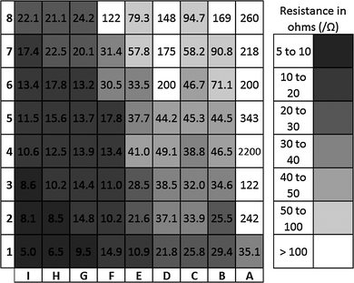 | ||
| Fig. 16 Resistance map measured using a two-point diode for all 72 allotted positions; numbers represent the resistance in ohms and the colour key corresponds to the resistance. | ||
 | ||
| Fig. 17 Plot of resistance in ohms against nitrogen percentage for the vanadium oxynitride positions analysed in column I. An exponential-type relationship, with a high degree of correlation (R = 0.929) was observed. | ||
The relationship between nitrogen incorporation and electrical resistance fit an exponential model, deviating from the linear relationship it was shown to hold with reflectivity. This is intuitive given the range of resistances observed, differing by several orders of magnitude across the film.
Side-on SEM images demonstrated greater thicknesses towards the bottom of the film that decreased in a Gaussian fashion towards the top end. As the conductivity of a film is directly proportional to its thickness, without incorporation of this factor, an accurate relationship cannot be contrived. The resistivity was therefore calculated for all positions along column I (Fig. 18)
 | ||
| Fig. 18 Plot of resistivity/K in ohm metres, where K is the unknown width of the diodes utilised in measuring the resistance against nitrogen percentage for the vanadium oxynitride positions analysed in column I. | ||
As the exact width of the diodes used in determining the resistance was not accurately measurable, merely the resistivity/diode width (K) could be represented. Nevertheless, a direct relationship between resistivity/K and nitrogen incorporation was observed with an approximate fit to a linear model. The lower degree of correlation in comparison with the reflectance relationship derived (Fig. 15) was possibly due to the incorporation of film thickness in the resistivity calculation.
Discussion/conclusion
A thin film, gradating from triclinic Magneli V8O15 to hexagonal V2O3 to a range of cubic VOxN1−x (0.23 < x < 0.53) phases was synthesised using a triple source of precursors: VCl4 [metal source], H2O [oxygen source], and NH3 [nitrogen source]. This was the first time cAPCVD had been used to synthesise a gradating mixed anion system. Rietveld refinement against XRD data, in conjunction with Vegard's law, allowed for the prediction of nitrogen content at each oxynitride position analysed. The predictions were in strong agreement with WDX analysis of corresponding positions, where a statistical comparison allowed the extraction of an associated error. XPS analysis of the front row showed a transition in phase from an oxide to an oxynitride in line with XRD analysis; however an oxidation state increase for each environment analysed was observed due to surface oxidation that occurs upon cool-down in the reactor after deposition. Raman analysis of the front row phases was also in agreement with those identified by XRD analysis of database literature examples.A Gaussian distribution of film thicknesses was observed, with the thickest parts of the film formed near the hottest point of the underlying carbon block on which it was heated inside the reactor. Optical studies showed the high reflectivity of all oxynitride positions analysed, typical for phases of metallic character. As a 0% transmittance was observed for the entire 300–2500 nm range and a consistently grainy surface with similar crystallite diameters was seen for all positions, a relationship between the nitrogen percentage and resistance along column I was formed with a high degree of correlation. Electrical resistivity determination verified the increase in metallic character of the oxynitride section with an increase in nitrogen incorporation. The sheet resistances seen were comparable to that of films formed via analogous APCVD routes in the literature,5–7 however, the electrical resistivities could not be directly compared as an accurate diode width used in their measurement was unobtainable.
Physical vapour deposition (PVD) has also been exploited to create combinatorial film systems where functional properties could be matched with phase content. Combinatorial PVD synthesised Ni–Fe–Cr ternary and Ni–Cr binary composites have been probed for mechanical hardness optimisation37 and high temperature PVD synthesised Mg–Ni hydrides for hydrogen storage optimisation.38 The combinatorial CVD approach gives a different phase distribution pattern compared with PVD systems. For example, the PVD is a line of sight process that tends to be a top-down projection onto a surface whereas the CVD set-up developed in this work gives a change in compositional profile associated with gases that run parallel to the substrate. Furthermore the reaction chemistry in CVD systems is different from PVD processes and may have advantages in making films that are easier to administer because of better adhesion and durability.
Combinatorial atmospheric pressure chemical vapour deposition was utilised to synthesise vanadium oxynitrides with a range of gradating oxygen content on a single film. Characterisation and functional property mapping allowed for the quantitative display of the detriment of higher oxygen incorporations upon the electrical conductivity and infrared reflective properties of the oxynitride.
The time required in synthesising a cAPCVD produced film containing an array of compositions and phases compared with the time taken to individually synthesise them via traditional or even robotic methods are orders of magnitude faster. When mapping techniques are used, such as XRD/Raman analysis with X–Y manoeuvrable stages, a rapid analysis of phase space is possible. Some physical properties can also be easily mapped, whereby a two-point diode can gauge an electrical resistance map of an entire film in a matter of minutes. Clearly, when multi phase/compositional cAPCVD synthesised films are investigated with mapping analysis techniques, the possibility for high-throughput determination of relationships for functional property optimisation of alternative mixed-ion systems are extensive.
| Technique | Positions Characterised |
|---|---|
| XRD | All 72 positions |
| WDX | 9 front positions; row A1-I1 & an additional 8 positions 1 mm either side of F1, G1, H1 & I1 |
| XPS | 9 front positions; row A1-I1 |
| Raman | 9 front positions; row A1-I1 |
| Side-on SEM | All 72 positions |
| UV-vis | 40 positions; columns A, C, E, G & I |
| Electrical resistance | All 72 positions |
Acknowledgements
Professor Ivan. P. Parkin wishes to thank the Royal Society and Wolfsen Trust for a merit award and express gratitude to Mr Kevin Reeves (UCL Archaeology) for assistance in SEM studies and Dr Steve Firth (UCL Chemistry) for his assistance in Raman spectroscopy studies.References
- G. Hyett and I. P. Parkin, Surf. Coat. Technol., 2007, 201(22–23), 8966 CrossRef CAS.
- T. P. Martin, K. Chan and K. K. Gleason, Thin Solid Films, 2007, 516, 681.
- G. Hyett, I. P. Parkin and M. A. Green, J. Am. Chem. Soc., 2007, 129, 15541 CrossRef CAS.
- I. P. Parkin and G. Elwin, J. Mater. Chem., 2001, 11, 3120 RSC.
- A. Newport, C. J. Carmalt, I. P. Parkin and S. A. O'Neill, Eur. J. Inorg. Chem., 2004, 21, 4286 CrossRef.
- G. Elwin and I. P. Parkin, Chem. Vap. Deposition, 2000, 6(2), 59 CrossRef.
- T. Maruyama and Y. Ikuta, J. Mater. Sci., 1993, 23, 5073 CrossRef.
- R. Binions, G. Hyett, C. Piccirillo and I. P. Parkin, J. Mater. Chem., 2007, 17, 4652 RSC.
- R. Binions, I. P. Parkin and C. Piccirillo, Surf. Coat. Technol., 2007, 201, 9369 CrossRef CAS.
- R. Binions, I. P. Parkin, C. Piccirillo and R. G. Palgrave, Chem. Vap. Deposition, 2008, 14, 33 CrossRef CAS.
- T. D. Manning and I. P. Parkin, Polyhedron, 2004, 23, 3087 CrossRef CAS.
- T. D. Manning, I. P. Parkin, M. E. Pemble, D. Sheel and D. Vernardou, Chem. Mater., 2004, 16(4), 744 CrossRef CAS.
- M.N. Field and I. P. Parkin, J. Mater. Chem., 2000, 10, 1863 RSC.
- P. Evans, M. E. Pemble, D. W. Sheel and H. M. Yates, J. Photochem. Photobiol., A, 2007, 189, 387 CrossRef CAS.
- L. Kritikos, L. Zambellis, G. Papadimitropoulos and D. Davazoglou, Surf. Coat. Technol., 2007, 201, 9334 CrossRef CAS.
- C. M. Lampert, Thin Solid Films, 1993, 236, 6 CrossRef CAS.
- G. Hyett, R. Binions and I. P. Parkin, Chem. Vap. Deposition., 2007, 13, 675 CrossRef CAS.
- L. Vegard, Z. Phys., 1921, 17, 5 Search PubMed; L. Vegard, Z. Kristallogr., 1928, 67, 239.
- H. M. Rietveld, J. Appl. Crystallogr., 1969, 2, 65 CrossRef CAS.
- B. H. Toby, J. Appl. Crystallogr., 2001, 34, 210 CrossRef CAS.
- D. Briggs and M. P. Seah, Practical Surface Analysis, John Wiley & Sons, Chichester, 2nd edn, 1990, p. 635 Search PubMed.
- INCA microanalysis system, http://www.X-raymicroanalysis.com/pages/main/inca.htm, last accessed 14th August 2008.
- P. Mogyorosi, L. B. Kiss, J. Kovacs, E. Sizil and I. Hevesi, Infrared Phys., 1986, 26, 197 CrossRef CAS.
- I. I. Timofeeva and L. K. Shvedova, J. Less-Common Met., 1964, 6, 326 CrossRef.
- R. E. Loehman, C. N. R. Rao and J. M. Honig, J. Phys. Chem., 1969, 73, 1781 CrossRef CAS.
- G. Hyett, M. Green and I. P. Parkin, J. Am. Chem. Soc., 2006, 128, 12147 CrossRef CAS.
- D. Borgmann, E. Hums, G. Hopfengartner, G. Wedler, G. W. Spitznagel and I. Rademacher, J. Electron Spectrosc., 1993, 63, 91 CrossRef.
- A. Glaser, S. Surnev, F. P. Netzer, N. Fateh, G. A. Fontalvo and C. Mitterer, Surf. Sci., 2007, 601, 1153 CrossRef CAS.
- A. Atrens and A. S. Lim, Appl. Phys. A: Mater. Sci. Process., 1990, 51, 411 CrossRef.
- V. Carlier, C. Poleunis, L. T. Weng, M. Sclavons, P. Bertrand, P. Franquinet and R. Legras, J. Adhesion Sci. Technol., 1995, 9, 859 CrossRef.
- F. Beguin, I. Rashkov, N. Manolova, R. Benoit, R. Erre and S. Depleux, Eur. Polym. J, 1998, 34, 905 CrossRef CAS.
- A. G. Aronov, D. N. Mirlin, I. I. Reshina and F. A. Chudnovskii, Fiz. Tverd. Tela, 1977, 19, 193 Search PubMed.
- N. N. Greenwood and A. Earnshaw, Chemistry of the Elements, Butterworth-Heinmann, Oxford, 2nd edn, 1997, pp. 961 and 983 Search PubMed.
- N. Kuroda and H. Y. Fan, Phys. Rev. B, 1977, 16, 5003 CrossRef CAS.
- D. N. Mirlin and I. I. Reshina, Fiz. Tverd. Tela, 1977, 19, 201 Search PubMed.
- R. J. Betsch, J. Cryst. Growth, 1986, 77, 210 CrossRef CAS.
- A. Rar, J. J. Frafjord, J. D. Fowlkes, E. D. Specht, P. D. Rack, M. L. Santella, H. Bei, E. P. George and G. M. Pharr, Meas. Sci. Technol., 2005, 16, 46 CrossRef CAS.
- S. Guerin, B. E. Hayden and D. C. A. Smith, J. Comb. Chem., 2008, 10, 37 CrossRef CAS.
| This journal is © The Royal Society of Chemistry 2009 |