High-resolution soft lithography of thin film resists enabling nanoscopic pattern transfer
Isaac W.
Moran
,
Dalton F.
Cheng
,
Sarav B.
Jhaveri
and
Kenneth R.
Carter
*
Polymer Science and Engineering Department, University of Massachusetts Amherst, Conte Center for Polymer Research, 120 Governors Drive, Amherst, Massachusetts 01003, USA. E-mail: krcarter@polysci.umass.edu; Fax: +1 413-545-008; Tel: +1 413-577-1416
First published on 19th November 2007
Abstract
Soft UV-imprint lithography at sub-micron dimensions was achieved in thin films of photopolymer resist. The imprinting was enabled by overcoming resist absorption by polydimethylsiloxane (PDMS) through surface treatment with a layer of (heptadecafluoro-1,1,2,2-tetrahydrodecyl)dimethylchlorosilane. Characterization of the composite molds was done by X-ray photoelectron spectroscopy, nanoindentation, and contact angle measurements. PDMS molds treated with fluoroalkylsilane layer were used to imprint into thin films (70–630 nm) of UV curable resins consisting of either polyurethanes or acrylates, replicating with high fidelity features over the surface of wafer substrates. The use of these highly conformal PDMS molds allowed the patterning of functional materials including gold and aluminium by a simple imprint lithographic technique. This is the first report of the use of modified PDMS surfaces in an imprint process that enables the transfer of sub-micron patterns to underlying layers for device structure fabrication. The patterned features were studied with atomic force microscopy, scanning electron microscopy, and optical microscopy.
Introduction
The need to enable high throughput, high fidelity nanoscale replication by economic means has fueled a surge in the development of nanopatterning techniques. Photolithography remains the industrial standard for large scale manufacturing and e-beam lithography retains dominance in producing the smallest critical dimensions,1 yet a number of other methods including dip pen lithography,2 block-copolymer templates,3microcontact printing (μCP),4 nanotransfer printing (nTP),5 and capillary force lithography6 have been extensively developed on a laboratory scale. In addition to the aforementioned methods, nanoimprint lithography (NIL) is a likely candidate for competing with photolithography in the large scale manufacturing of features below 100 nm.1,7 While impressive milestones in feature size8 and automation7 have been accomplished by traditional thermal and UV-assisted NIL processes, the potential ease-of-use and effectiveness in large area patterning offered by “soft” imprint-lithography (soft-NIL) have made it an ideal testing ground for new imprint technologies.In soft-NIL, a cross-linked, elastomeric mold is used to pattern a UV curable photopolymer resin that has been applied to an underlying substrate. Curing is usually achieved by exposure to UV light which initiates a radical cross-linking reaction hardening the resin while in contact with the mold. As with other forms of soft-lithography, soft-NIL exploits the special surface and mechanical properties of molds consisting of polydimethylsiloxane (PDMS). The performance of PDMS molds is derived from its low modulus (∼2–3 MPa)9 and low surface energy (20 mJ m−2).10 These properties allow a PDMS mold to produce consistent nanoscale imprints on the surface of resists, over large contact areas regardless of a substrate's topographic uniformity by conforming to the surface during contact and yielding during release.9a,11 Imprinting using PDMS has proven to be an effectual means for replicating nanoscale features on the surface of resists with dimensions on the order of 40 nm, and in one report as small as 2 nm.12 This mode of imprinting is shown in Scheme 1 as case I-type soft-NIL. In case I, patterns are successfully imaged (Scheme 1a) into the top layer of an otherwise thick resist layer, usually with imprint depth comprising less than half the total thickness of the resist (Scheme 1b). Attempts to transfer this pattern to the underlying substrate, for example by anisotropic plasma etch techniques, results in total obliteration of the pattern before selective etch of the substrate can occur—therefore there is no pattern transfer (Scheme 1c). The tendency of pattern obliteration is exacerbated as the critical dimension of the features becomes smaller than 100 nm. Similar attempts to utilize conventional lift-off pattern transfer techniques results in no pattern transfer for the same reason. In case II, patterns are also successfully imaged but into a thin resist layer (Scheme 1a), resulting in imprint depths on the same order as the thickness of the resist film (Scheme 1b). Patterned thin films have little or no residual layer and pattern transfer to the underlying substrate by conventional etch techniques is achievable (Scheme 1c).
 | ||
| Scheme 1 Attempts to use soft-NIL for the fabrication of device structures of sub-micron dimensions are classified into two types: case I, where the nanopattern is successfully transferred to the surface of the resist layer, but because of the resist thickness it is impossible to transfer the pattern into the underlying substrate using anisotropic etching techniques and case II, where the nanopattern is made into a thin film of resist and pattern transfer to underlying substrate is successful. | ||
To date, two issues have restricted soft-NIL from being used for Case II imprinting and therefore prevented the advanced fabrication of device structures. The first being the low modulus of PDMS, which can result in collapse of high aspect ratio features, and the second being the high permeability of PDMS to organic compounds resulting in absorption of non-polar resists with concurrent swelling and distortion of the PDMS mold.13 Whereas feature collapse can be overcome by use of “h-PDMS”, a highly crosslinked version of the original elastomer with corresponding higher modulus (9 MPa, surface hardness 2.6% of glass),10a,14 resist absorption into the mold essentially negates the patterning of thin resist films. This is a critical issue as thin film resists are necessary for the subsequent pattern transfer process to the underlying substrate. In fact, the inability to imprint into thin organic-based resists negates the utility of Soft-NIL in nanofabrication. Accordingly, with the exception of capillary force lithography, which requires imprint times on the order of 1 day,6 no PDMS-based soft-UV imprint lithography technique has demonstrated the capacity to use imprinted patterns to fabricate useful structures via resist pattern transfer. While we have examined the use of fluoropolymer elastomer molds in soft-NIL to overcome many of these issues,15 we wish to enable the use of inexpensive, widely available PDMS as imprint molds.
This report addresses the issue of organic resist absorption by implementation of an easily achievable hybrid PDMS–silicon oxide mold. Oxygen plasma is used to convert the surface of a PDMS mold to an impermeable inorganic SiOx layer which is preserved by a fluorinated alkyl silane (FAS) coating. The resulting hybrid mold retains the high conformability of bulk PDMS but is effective in patterning thin films of various photopolymer compositions with thickness of a few hundred nm. While plasma oxidized PDMS (PDMSox) has been previously utilized in μCP to form hydrophilic stamps or serve as a hydroxy terminated surface for the anchoring of hydrophilic functionality,16 no investigation has been done with regard to exploiting the resulting oxide layer as a resist absorption barrier during imprint lithography. Similarly, the use of chemisorbed fluorinated alkyl silanes on PDMS has facilitated μCP of both polar and non-polar inks17a but has not yet been applied to soft-NIL.
Experimental
Materials
Single sided polished 1″ silicon wafers were purchased from Silicon Quest International, Inc. Dow Corning polydimethylsiloxane (PDMS) precursor (Sylgard™184) was used. Norland Optical 60 (η = 0.3 Pa s) photopolymer resin was acquired from Norland Products. Methanol from Fisher, (heptadecafluoro-1,1,2,2-tetrahydrodecyl)dimethylchlorosilane from Gelest, ethoxylated bisphenol A dimethacrylate from Sartomer, 2-ethyl-2-(hydroxymethyl)-1,3-propanediol triacrylate, 2,2-dimethoxy-2-phenylacetophenone, 1-vinyl-2-pyrrolidone 99%, 2-hydroxyethyl methacrylate (HEMA) 98%, α,α′-azoisobutyronitrile (AIBN) 98%, 1-dodecanethiol 98%, 3-(trimethoxysilyl)propyl methacrylate 98%, and propylene glycol methyl ether acetate (PGMEA), from Sigma Aldrich were used as received.Characterization
Water contact angle measurements were observed using an AST Products, Inc. contact angle goniometer equipped with a Hamilton syringe having a flat-tipped needle. Deionized water was used as the probe fluid after filtering numerous times through a 20 nm syringe filter. The drop size was 1.00 μL. All reported values are the average of 3 to 5 measurements of drops on different areas of the sample surface. The modified surfaces exhibited homogeneous coating as evidenced by a tight distribution of measured contact angles; measured values were typically within ±1° of the average. X-Ray photoelectron spectra (XPS) were recorded on a Physical Electronics Quantum 2000 with Al Kα excitation (50 W). Spectra were obtained at a takeoff angle of 45° (between the plane of the surface and the entrance lens of the detector optics). Film thickness was measured by reflectance with a Filmetrics F20 Thin Film Measurement System. The reported values are an average of at least 10 measurements over the entire surface with a typical standard deviation of ±3 nm. Images of the imprinted features were acquired with a JEOL JSM 6320F field emission gun scanning electron microscope (SEM). Atomic force microscopy (AFM) images were collected on a Digital Instruments Dimension 3000 Nanoscope in intermittent contact mode under ambient conditions using silicon cantilevers and a scan rate between 0.5 to 1 μm s−1.Mold preparation
The Sylgard 184 base and curing agent PDMS precursor components were mixed together in a 10 : 1 ratio, degassed, cast over a master composed of patterned aluminium on silicon wafers to a mold thickness of about 3.5 mm, and cured for 12 hr at 65 °C. After curing, the PDMS was carefully separated from the master and the patterned surface was exposed to 12 MHz RF O2 plasma in a Harrick PDC-001 Plasma Cleaner under 100 mbar of oxygen at 30 W for 7 min forming a surface layer of SiOx silica. Molds supported on glass slides were then sealed in air-tight vessels with 0.5 ml of (heptadecafluoro-1,1,2,2-tetrahydrodecyl)dimethylchlorosilane and heated at 85 °C for 24 hr to react with the SiOx layer.Determination of silica layer thickness
Measurement of the thin silica layer formed by plasma treatment of PDMS was done following the procedure developed by Stafford et al. for determining the modulus or conversely, the thickness of thin films on bulk PDMS.18 A flat, featureless, rectangular sample of the cured PDMS (5.08 cm × 2.54 cm × 0.635 cm) was placed on a microscope slide and plasma-treated for 7 min to form an equivalent layer of SiOx as that on the patterned molds. To measure the oxide layer thickness, the PDMSox sample was compressed along its short axis, causing a buckling instability to form due to the modulus mismatch between the soft rubbery substrate and the newly formed stiff silica layer. Small angle light scattering using a He–Ne laser with wavelength 632 nm was employed to obtain the diffraction pattern of spots from the buckling pattern. The distance between the spots allowed for calculation of the wavelength of the buckles, from which the thickness of the layer could be estimated assuming the Young's modulus of the porous silica layer and the PDMS substrate to be 70 GPa19 and 1.5 MPa, respectively, and Poisson's ratio of the silica layer and the PDMS substrate to be 0.17 and 0.5, respectively.Solvent absorbance measurements
Slabs of PDMS, PDMSox, and PDMSF-ox, were weighed. A glass tube (diameter = 6 mm) filled with 2.3 ml of PGMEA was placed on top of the slab and kept in contact for 10 min after which the slab was removed and excess solvent was quickly blown off by a stream of N2 (∼1 sec). The slab was immediately weighed a second time with the difference in mass representing the total amount of solvent absorbed. 3 measurements were taken for each surface type and the flux calculated as F = (m/t)A, m = mass absorbed, t = time, and A = area described by the tube.It should be noted that mass loss from the mold can occur by extraction of mobile PDMS oligomers into the solvent reservoir. However, collection and NMR analysis of the PGMEA after an absorbance measurement did not reveal any siloxane content. After the solvent was evaporated there was a small residue that was determined by NMR to be oligomeric siloxane. The small amount was calculated to be ∼0.35% of the total mass taken up by the mold and therefore considered to be insignificant.
Synthesis of poly(hydroxyethylmethacrylate) (PHEMA)
Ethanol (7.5 mL) was taken in a test-tube and nitrogen was bubbled through for 5 minutes. AIBN (0.07 g, 0.43 mmol), HEMA (5.37 g, 5 mL, and 41.31 mmol) and dodecane thiol (0.43 g, 0.5 mL) were dissolved in ethanol and the solution was heated and stirred under N2 at 60 °C for 4 hours. The solution was cooled and precipitated dropwise in hexanes. The polymer was filtered, washed with hexanes and dried to obtain polyhydroxyethylmethacrylate (PHEMA) (4.5 g, 84%) as a white solid. GPC data (in DMF): Mn = 32![[thin space (1/6-em)]](https://www.rsc.org/images/entities/char_2009.gif) 353, PDI = 1.37.
353, PDI = 1.37.
Acrylate/methacrylate photopolymer formulation (PP)
Photocureable monomer formulation was prepared by mixing ethoxylated bisphenol A dimethacrylate 76.5 wt%, 2-ethyl-2-(hydroxymethyl)-1,3-propanediol triacrylate 23.2 wt%, and 2,2-dimethoxy-2-phenylacetophenone 2.5 wt% as initiator. PP viscosity = 1 Pa s.UV imprinting with PDMSF-ox molds
2″ silicon wafers were diced into squares of approximately 1 in.2 Each diced substrate was prepared for imprinting by washing with acetone and drying under N2. A solution of PHEMA (6.5 wt% in methanol) was spin-coated at 3000 rpm for 10 sec followed by baking at 130 °C for 30 sec forming a 180 nm thick lift-off film. An adhesion promoter, 3-(trimethoxysilyl)propyl methacrylate, was then spin-coated at 3000 rpm for 10 sec and the wafer was baked at 130 °C for 2 min. Excess adhesion promoter was rinsed off by spinning the mold while applying a pure stream of PGMEA for 15 sec at 3000 rpm followed by drying with N2. Photopolymer, either Norland Optical 63 or PP, diluted in PGMEA to specific concentrations and filtered through a 0.45 μm syringe filter, was then spin-coated at 3000 rpm for 15 sec. Immediately thereafter a treated PDMS mold was placed directly on the thin film and pressed lightly (approximately 5 g force) for several seconds to initiate propagation of interfacial contact between the two surfaces. Exposure to 365 nm UV light from a 500 W OAI UV lamp under a N2 blanket for 12 min cured the imprinted photopolymer leaving patterns after removal of the PDMS mold.Etching, metal deposit, lift-off
Patterned films were etched for about 23 sec in a South Bay Technologies RIE-200 Reactive Ion Etcher under 300 mTorr of O2 plasma at 180 W until the underlying silicon wafer was exposed in the recessed regions throughout the imprint. Etched wafers were coated with metal by vacuum evaporation. Lift-off was achieved by sonication in warm methanol for 30 to 60 min followed by a rinse with fresh methanol.Results and discussion
To allow successful nanoimprinting of thin films a scheme was devised to render the surface of PDMS molds impermeable to organics yet maintain the overall bulk elastomeric properties of the material. This was achieved by following the procedure depicted in Fig. 1. PDMS molds were prepared by casting a siloxane prepolymer on a patterned silicon master and curing for 12 hr at 65 °C. After removal from the master, the surface of the cured PDMS mold was exposed to O2 plasma which created a thin surface layer of silica (SiOx). A fluorinated silane layer was applied by vapor phase reaction of the hydroxy activated silica surface with a fluorinated chlorosilane. | ||
| Fig. 1 Schematic representation of fluorinated oxide PDMS mold formation. PDMS prepolymer was mixed and cast onto a Si master. After curing, the PDMS mold was released and exposed to O2 plasma to form a silica layer. A final FAS layer was vapor deposited to help preserve the oxide barrier and maintain low surface energy. | ||
The thickness and density of the plasma grown silica layer is a function of the O2 exposure time. Through simple experimentation it was determined that exposure for approximately 7 min at a power of 30 Watts produced a SiOx layer that was dense enough to prevent the absorption of resist yet thin enough to maintain a flexibility capable of withstanding multiple imprints without cracking. An optimal oxide thickness of approximately 16 nm was estimated via its diffraction grating following the work of Stafford et al. for determining film dimensions on bulk PDMS.18
Utilizing plasma treated molds for imprinting directly after the O2 plasma treatment is possible, however, the silica layer is unstable due to the presence of oligomeric low surface energy PDMS present within the network which, over time, migrates to the surface and reacts with SiOx, effectively breaking down the resist barrier by reverting the surface back to PDMS.20Fig. 2, square symbols, illustrates the gradual loss of surface hydrophilicity with time measured by the water contact angle for a PDMS surface which has been plasma treated for 7 min. The plasma treated surface reverts back to its native level in less than 1 hr. This change in surface composition must be prevented to produce molds which remain useful for extended periods of time. An attempt was made to overcome the reversion of PDMSox to PDMS by removal of oligomeric PDMS through extended Soxhlet extraction. Unfortunately, the extracted molds performed poorly due to a decrease in plasticization as a consequence of the removal of oligomeric PDMS and concurrent increase in mold modulus. While the higher modulus, extracted molds would conform to resin coated planar surfaces under slight pressure, the applied force caused disruptions to the resist layer resulting in large variations in residual layer thickness after imprinting.
 | ||
| Fig. 2 Change in the advancing (open symbols) and receding (closed symbols) contact angles with deionized water over time for oxidized PDMS (PDMSox, squares) and fluorinated oxidized PDMS (PDMSF–ox, circles) surfaces. | ||
Preservation of the resist barrier was achieved by reacting the oxidized mold with a FAS ((heptadecafluoro-1,1,2,2-tetrahydrodecyl)dimethyl chlorosilane) in vapor phase to form a fluorinated layer on the mold surface.17 It has been considered that permeation of the PDMS mold by gaseous fluorosilane may have also resulted in a fluorinated zone on the interior wall of the oxide layer thus producing an inner barrier to the encroaching free oligomers.16b Surface treatments using di- and tri-chlorosilanes are known to suffer from crosslinking siloxane polymerization reactions in competition with surface functionalization and can give undesirable rough surfaces.21 A mono-chlorosilane was chosen to eliminate this possibility. The fluorinated layer should also produce a lower surface energy (∼15 mJ m−2) surface than that of PDMS.17bFig. 3 shows the progression in surface functionality from bulk PDMS to PDMSox to fluorinated oxide PDMS (or PDMSF-ox) as detected by X-ray photoelectron spectroscopy (XPS) survey scans. These spectra demonstrate that the initially high carbon content of bulk PDMS is greatly diminished after plasma exposure by oxidation of the dimethylsiloxane to an oxygen rich SiOx surface. Successful FAS layer formation was verified by the appearance of fluorine peaks at 690 eV and 890 to 810 eV after reaction with the fluorinated chlorosilane.
 | ||
| Fig. 3 Progression in XPS spectra for PDMS surface functionality. | ||
Water contact angle measurements were also used to monitor the change in surface functionality during mold preparation. Here a typical contact angle of 106° was measured for bulk PDMS while complete wetting (contact angle <10°) occurred on the PDMSox surface, Fig. 4. After fluorinated layer formation, PDMSF-ox surfaces gave a high value of 111° which is in agreement with other similarly prepared surfaces.22 Formation of the fluorinated layer effectively stabilized the surface hydrophobicity as shown in Fig. 2, open circles, where it is seen that the water contact angle changes little over 50 min thus providing a lasting barrier to resist absorption, which is needed for prolonged mold use. Solvent absorbance measurements were also performed to establish how treated PDMS acted as a barrier to absorption. Table 1 lists the flux of PGMEA into 3 forms of unpatterned PDMS slabs: 1) a native, untreated surface, 2) a plasma oxidized surface, and 3) a fluorinated surface. It was found that the freshly oxidized and fluorinated surfaces were both effective in reducing the flux of PGMEA by a factor of 2. Typically, with the exception of one study,17asiloxane monolayers assembled on PDMSox have been used in μCP to impart hydrophiliticy in order to increase uptake of polar inks. The hydrophobic, or more specifically, highly electronegative, oleophobic fluorinated surface used in our approach is designed to decrease or even eliminate absorption of the hydrophobic resist material. The complete composite mold, structured as PDMS/SiOx/FAS, was designed to provide superior molding capabilities through a resist impermeable, higher modulus, lower energy surface than the original Sylgard 184 PDMS material. The PDMSF-ox composite molds still retain bulk elastomeric properties allowing high conformal contact with substrates coated with low viscosity resins.
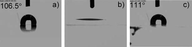 | ||
| Fig. 4 Contact angle images of deionized water on a) unmodified PDMS, b) plasma treated PDMS (PDMSox), and c) fluorinated oxide PDMS (PDMSF–ox). | ||
| Surface | Flux/mg m2 s−1 |
|---|---|
| PDMS | 1.04 E–09 |
| PDMSox | 4.34 E–10 |
| PDMSF–ox | 5.18 E–10 |
Once the molds were prepared, they were used to pattern thin films of an UV-curable photopolymer. The imprinting process, as illustrated by Fig. 5, began by applying a lift-off layer consisting of polyhydroxyethylmethacrylate (PHEMA) to the substrate. This surface was treated with an adhesion promoter layer by spin coating and curing 3-(trimethoxysilyl)propyl methacrylate on the surface of the PHEMA layer. To this surface was spun a thin film of a UV-curable photopolymer followed immediately by placement of the PDMSF-ox mold. After the contact line of the interface was observed to propagate between the mold and resin, the photopolymer was cured under UV light (365 nm) in a nitrogen atmosphere. No additional pressure was applied to the mold as it was found that conformal contact of the mold and resin was sufficient to faithfully replicate the imprinted pattern. Release of the mold yielded patterned substrates bearing replicated features consisting of cured photopolymer with dimensions ranging in microns to hundreds of nm.
 | ||
| Fig. 5 Imprint lithography using PDMSF–ox molds. Using a PDMSF–ox mold, features were imprinted into a thin film of spun photopolymer resin on top of a polyHEMA release layer. After UV curing of the resin the mold was released and reactive ion etching was used to break through to the underlying Si surface. Metal was vapor deposited and lift-off in warm methanol produced patterned metal features. | ||
Dense imprint patterning over large areas was accomplished using molds measuring approximately 3.3 cm2. The high degree of fidelity in the pattern replication is displayed in Fig. 6, which shows the sequence of master, mold, and imprint. The photopolymer used in this example was Norland Optical 60 (NO60), a urethane-based optical adhesive prepolymer, diluted in PGMEA and spun to a thickness of 630 nm. Attempts to imprint NO60 with an untreated PDMS mold resulted in complete resin absorption in the contact area preventing any pattern formation. However, a PDMSF-ox mold allowed the successful replication of the entire field with no observed defects due to absorption or lack of contact between the mold and substrate. The same mold was used to make several imprints over multiple days without loss of performance.
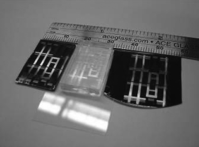 | ||
| Fig. 6 Master (left), mold (center), and imprint (right) demonstrating the high fidelity capability of PDMSF–ox molds over large areas. The patterned area shown measures over 3 cm2. | ||
Furthermore, PDMSF-ox molds are not specific for one type or class of resist as the fluorinated silica layer was demonstrated to be an effective barrier to other photopolymer formulations. For example, high quality imprints were also created using an acrylate/methacrylate-based photopolymer previously used for contact molding.23 Integrity of the chemical composition of the imprinting surface was verified by XPS analysis of new and used molds (Fig. 7) demonstrating the durability of this surface modification. We observed no loss of fluoroalkylsilane after multiple imprints.
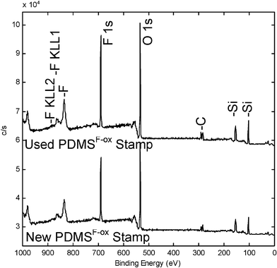 | ||
| Fig. 7 XPS spectra of a freshly prepared (bottom) and used (top) PDMSF–ox mold. The consistency between both spectra illustrates the durability of the fluorinated oxide layer to the imprinting process. | ||
Examination of the features imprinted with PDMSF-ox by scanning electron microscopy (SEM) revealed successful replication of approximately 550 nm tall lines measuring from 2 microns to approximately 300 nm (Fig. 8a,b) in width. Negative trench features were also faithfully reproduced. The imprinted lines and trenches were further characterized by atomic force microscopy (AFM, Fig. 9). Tightly packed lines with heights of 573 nm and trenches with depths of 100 nm were easily resolved as determined by cross section analysis.
 | ||
| Fig. 8 SEM micrographs of line (a,b) and trench (c,d) features imprinted into photopolymer resin. a) Lines with varying widths ranging from 2 μm down to 300 nm. b) Close packed 600 nm lines. c) An array of close packed trenches varying from 500 nm to 300 nm. d) Close packed 400 nm trenches. | ||
 | ||
| Fig. 9 AFM imaging and sectional profile of a) 573 nm tall lines and b) 100 nm deep trenches imprinted into a 600 nm thick film of NO60. | ||
Use of soft-NIL to fabricate metal structures was carried out as illustrated in Fig. 5. After molding the resist layer, reactive ion etching was used to break through the remaining residual photopolymer and underlying PHEMA lift-off layer. Metal (either gold or aluminium) was then deposited by vapor deposition followed by lift-off of the PHEMA layer in warm methanol with sonication. The resulting patterned metallic structures consisting of both gold and aluminium are displayed in Fig. 10. SEM characterization of the metal structures formed by lithography verified the precision of this fabrication process (Fig. 10b–d). Both gold and aluminium lines in the range of 2 microns to ∼300 nm were faithfully replicated over the entire expanse of the imprinted region.
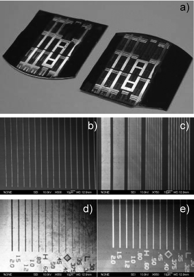 | ||
| Fig. 10 Large area fabrication of metallic structures on 1 inch silicon wafer substrates. a) Full pattern transfer of gold structures (left) and aluminium (right). SEM images of b) isolated gold lines ranging from 2.0 μm (right) to 300 nm (left), c) close packed gold gratings ranging from 2.0 μm (right) to 500 nm (left) on silicon, d) isolated aluminium trenches ranging from 2.0 μm (left) to 300 nm (right) on silicon, and e) isolated aluminium lines ranging from 2.0 μm (left) to 300 nm (right) on silicon. | ||
Even though gold structures have been patterned by other forms of soft-lithography, such as nTP,5 successful replication in these cases requires the templating of surface-anchored thiols which is not effective for the transfer printing of other useful metals like aluminium. Conversely, using this new process, in principle, allows the use of this simple process to pattern virtually any material that can be deposited over the patterned lift-off layer (metals, oxides, organics, etc.).
Features imprinted in the above examples had a height/depth on average of about 500 nm and were found to be best replicated using resist films of similar thickness. However, in order to enable the patterning of smaller features it is necessary to selectively pattern ultra-thin (<100 nm) films and this concern has been largely neglected by researchers in this field. Further studies were conducted to probe the limitations of this new technique with respect to resist film thickness. To probe the patterning of ultra-thin films, a new master with arrays of squares and pillars of approximately 20 nm in height and varying lateral dimensions was used to cast a PDMSF-ox mold. This mold was used to successfully imprint into a 293 nm thick film of NO60 with the resulting defect free features clearly visible by optical microscopy (Fig. 11a). The lateral dimensions for imprinted structures increase from 1 μm in the left-most set of pads to 2.5 μm in the central pads to 4 μm in the right most pads. The smallest imprinted pillars, unresolved by the optical microscope, are revealed by AFM demonstrating uniform replication of features with a height of only 20 nm as seen in Fig. 12. Fig. 11b shows micrographs of square and cylinder features imprinted into a 70 nm thick film of NO60, which, to the best of our knowledge, represents the thinnest resist film successfully imprinted by a PDMS mold. A few defects are visible in this imprint, which are due to contamination by dust particles. Regardless, this work suggests that imprinting with PDMSF-ox molds may only be limited by feature dimensions and not film thickness.
 | ||
| Fig. 11 Optical micrographs of square and cylinder features imprinted with PDMSF–ox molds into NO60 films spun to thickness of a) 293 nm and b) 70 nm. | ||
 | ||
| Fig. 12 AFM imaging and sectional profile of 20 nm tall, 1 μm wide cylinders imprinted into a 293 nm thick film of NO60. | ||
Conclusion
Effective and simplified lithographic pattern transfer and metallic structure fabrication has been accomplished. This has been enabled by the creation of PDMS molds capable of imprinting thin films of commonly available organic photopolymer resists. Treatment of an oxidized PDMS surface with a fluorinated chlorosilane yielded a stable fluorinated PDMS surface which was an effective barrier to photopolymer resist absorption. Without such treatment, PDMS molds are ineffective in patterning resists in soft-nanoimprint lithography. These surface-treated molds allowed for the advantageous retention of the low modulus of PDMS, and hence its high conformability, to enable high fidelity, defect free imprints over large surface areas. The ability to imprint multiple resist formulas using a commercially available PDMS composition and simple surface treatments greatly extends the scope and cost-effective versatility of soft-nanoimprint lithography. Application of PDMSF-ox molds allowed UV soft-imprint lithography to be performed on the thinnest resist films reported to date—a key requirement for efficient sub-micron, high fidelity pattern transfer. Due to the low resist film thickness used in this study, imprinted patterns were easily and reliably used to fabricate gold and aluminium structures and can easily be extended to other materials. Development of this process could potentially lead to highly economical, large scale imprint lithography for the fabrication of nanostructured active materials. Further work by our group on the fabrication of functional electronic devices with this method is forthcoming.Acknowledgements
This research was kindly supported by the NSF Nanoscale Science and Engineering Center (DMI-0531171) as well as the NSF Material Research Science and Engineering Center (MRSEC) (DMR-0213695) both at the University of Massachusetts Amherst. The Nanoimprint Lithography Laboratory recently established at the University of Massachusetts Amherst is supported by a grant from the NSF Major Research Instrumentation (MRI) program (DMR-0606391). The authors would also like to thank the 3 M Corporation for generous support through a non-tenure faculty award.References
- B. D. Gates, Q. Xu, M. Stewart, D. Ryan, C. G. Willson and G. M. Whitesides, Chem. Rev., 2005, 105, 1171–1196 CrossRef CAS.
- R. D. Piner, J. Zhu, F. Xu, S. H. Hong and C. A. Mirkin, Science, 1999, 283, 661–663 CrossRef CAS.
- G. Krausch and R. Magerle, Adv. Mater., 2002, 14, 1579 CrossRef CAS.
- (a) A. Kumar and G. M. Whitesides, Appl. Phys. Lett., 1993, 63, 2002–2004 CrossRef; (b) Y. N. Xia and G. M. Whitesides, J. Am. Chem. Soc., 1995, 117, 3274–3275 CrossRef CAS; (c) Y. N. Xia and G. M. Whitesides, Annu. Rev. Mater. Sci., 1998, 28, 153–184 CrossRef CAS.
- Y. L. Loo, R. L. Willett, K. W. Baldwin and J. A. Rogers, J. Am. Chem. Soc., 2002, 124, 7654–7655 CrossRef CAS.
- (a) K. Y. Suh, Y. S. Kim and H. H. Lee, Adv. Mater., 2001, 13, 1386–1389 CrossRef CAS; (b) C. M. Bruinink, M. Péter, P. A. Maury, M. de Boer, L. Kuipers, J. Huskens and D. N. Reinhoudt, Adv. Funct. Mater., 2006, 16, 1555–1565 CrossRef CAS.
- D. J. Resnick, S. V. Sreenivasan and C. G. Willson, Mater. Today, 2005, 8, 34 CrossRef CAS.
- M. D. Austin, H. X. Ge, W. Wu, M. T. Li, Z. N. Yu, D. Wasserman, S. A. Lyon and S. Y. Chou, Appl. Phys. Lett., 2004, 84, 5299–5301 CrossRef CAS.
- (a) A. Bietsch and B. Michel, J. Appl. Phys., 2000, 88, 4310–4318 CrossRef CAS; (b) H. Saechtling, International Plastics Handbook: for the Technologist, Engineer, and User, Carl Hanser, Munich, 3rd edn, 1995 Search PubMed; (c) S. J. Clarson, J. A. Semlyen, Siloxane polymers, Prentice Hall, Englewood Cliffs, NJ, 1993 Search PubMed.
- (a) C. J. Drummond and D. Y. C. Chan, Langmuir, 1997, 13, 3890–3895 CrossRef CAS; (b) D. W. v. Krevelen and P. J. Hoftyzer, Properties of polymers, their estimation and correlation with chemical structure, Elsevier Scientific Pub. Co., Amsterdam; New York, 2nd edn, 1976 Search PubMed.
- Y. N. Xia and G. M. Whitesides, Angew. Chem., Int. Ed., 1998, 37, 551–575 CrossRef CAS.
- (a) F. Hua, A. Gaur, Y. G. Sun, M. Word, N. Jin, I. Adesida, M. Shim, A. Shim and J. A. Rogers, IEEE Trans. Nanotechnol., 2006, 5, 301–308 CrossRef; (b) F. Hua, Y. G. Sun, A. Gaur, M. A. Meitl, L. Bilhaut, L. Rotkina, J. F. Wang, P. Geil, M. Shim, J. A. Rogers and A. Shim, Nano Lett., 2004, 4, 2467–2471 CrossRef CAS; (c) M. Bender, U. Plachetka, J. Ran, A. Fuchs, B. Vratzov, H. Kurz, T. Glinsner and F. Lindner, J. Vac. Sci. Technol., B, 2004, 22, 3229–3232 CrossRef CAS; (d) W. M. Choi and O. O. Park, Microelectron. Eng., 2004, 73–74, 178–183 CrossRef CAS.
- (a) J. N. Lee, C. Park and G. M. Whitesides, Anal. Chem., 2003, 75, 6544–6554 CrossRef CAS; (b) J. C. McDonald, D. C. Duffy, J. R. Anderson, D. T. Chiu, H. K. Wu, O. J. A. Schueller and G. M. Whitesides, Electrophoresis, 2000, 21, 27–40 CrossRef CAS.
- T. W. Odom, J. C. Love, D. B. Wolfe, K. E. Paul and G. M. Whitesides, Langmuir, 2002, 18, 5314–5320 CrossRef CAS.
- J. P. Rolland, E. C. Hagberg, G. M. Denison, K. R. Carter and J. M. De Simone, Angew. Chem., Int. Ed., 2004, 43, 5796–5799 CrossRef CAS.
- (a) D. C. Trimbach, M. Al-Hussein, W. H. de Jeu, M. Decre, D. J. Broer and C. W. M. Bastiaansen, Langmuir, 2004, 20, 4738–4742 CrossRef CAS; (b) E. Delamarche, C. Donzel, F. S. Kamounah, H. Wolf, M. Geissler, R. Stutz, P. Schmidt-Winkel, B. Michel, H. J. Mathieu and K. Schaumburg, Langmuir, 2003, 19, 8749–8758 CrossRef CAS; (c) E. Delamarche, M. Geissler, A. Bernard, H. Wolf, B. Michel, J. Hilborn and C. Donzel, Adv. Mater., 2001, 13, 1164 CrossRef CAS.
- (a) R. B. A. Sharpe, D. Burdinski, J. Huskens, H. J. W. Zandvliet, D. N. Reinhoudt and B. Poelsema, J. Am. Chem. Soc., 2005, 127, 10344–10349 CrossRef CAS; (b) M. K. Chaudhury and G. M. Whitesides, Science, 1992, 255, 1230–1232 CAS.
- C. M. Stafford, C. Harrison, K. L. Beers, A. Karim, E. J. Amis, M. R. Vanlandingham, H. C. Kim, W. Volksen, R. D. Miller and E. E. Simonyi, Nat. Mater., 2004, 3, 545–550 CrossRef CAS.
- H. Hillborg, N. Tomczak, A. Olah, H. Schonherr and G. J. Vancso, Langmuir, 2004, 20, 785–794 CrossRef CAS.
- H. Hillborg, J. F. Ankner, U. W. Gedde, G. D. Smith, H. K. Yasuda and K. Wikstrom, Polymer, 2000, 41, 6851–6863 CrossRef CAS.
- G. Y. Jung, Z. Y. Li, W. Wu, Y. Chen, D. L. Olynick, S. Y. Wang, W. M. Tong and R. S. Williams, Langmuir, 2005, 21, 1158–1161 CrossRef CAS.
- M. J. Pellerite, E. J. Wood and V. W. Jones, J. Phys. Chem. B, 2002, 106, 4746–4754 CrossRef CAS.
- (a) T. A. von Werne, D. S. Germack, E. C. Hagberg, V. V. Sheares, C. J. Hawker and K. R. Carter, J. Am. Chem. Soc., 2003, 125, 3831–3838 CrossRef CAS; (b) G. M. McClelland, M. W. Hart, C. T. Rettner, M. E. Best, K. R. Carter and B. D. Terris, Appl. Phys. Lett., 2002, 81, 1483–1485 CrossRef CAS.
| This journal is © The Royal Society of Chemistry 2008 |