Field-dependent carrier generation in bulk heterojunction solar cells
Z. E.
Ooi
ab,
T. L.
Tam
a,
A.
Sellinger
a and
J. C.
deMello
*b
aInstitute of Materials Research and Engineering (IMRE) and Agency for Science, Technology and Research (A*STAR), 3 Research Link, Singapore 117602
bDept. of Chemistry, Imperial College London, Exhibition Road, South Kensington, London, UK SW7 2AY. E-mail: j.demello@imperial.ac.uk
First published on 26th June 2008
Abstract
We analyse the current–voltage (J–V) characteristics of bulk heterojunction devices based on two different materials systems: (i) poly[2-methoxy-5-(3′,7′-dimethyloctyloxy)-1,4-phenylenevinylene]:(6,6)-phenyl-C61-butyric acid methyl ester (MDMO-PPV:PCBM); and (ii) poly[N-(2′-decyltetradecyl)carbazole]-2,7-diyl: bis(2-(1-ethylhexyl-4,5-dicyanoimidazol-2-yl)vinyl) benzo[c]1,2,5-thiadiazole (PCz:EV-BT). The J–V characteristics were recorded in the dark and light using a pulsed technique that ensured the two sets of measurements were obtained at equal temperatures. In each case, the dark current was subtracted from the photocurrent to obtain a corrected photocurrent Jph that excludes the photovoltage-induced injection current and is thus due solely to the flux of incident photons. The Jph–V response of the MDMO-PPV:PCBM was consistent with a model in which all photogenerated excitons dissociate into free carriers irrespective of the internal field strength. The Jph–V response of the PCz:EV-BT device, by contrast, was consistent with a model in which an electric field is required to initiate appreciable charge separation. The different behaviour is attributable to the different energy offsets of the frontier orbitals responsible for charge separation: 1.3 eV for MDMO-PPV:PCBM compared to just 0.4 eV for PCz:EV-BT.
Introduction
Organic solar cells offer a promising route to low-cost, sustainable electricity generation.1 Bulk heterojunction solar cells based on intimate blends of electron- and hole-transporting materials are of particular interest as they have yielded the highest power efficiencies to date (>5%).2 However, their performance still lags far behind conventional silicon solar cells, and there is interest in experimental measurements that can provide new insight into the physical processes that govern – and limit – the operation of organic devices.In bulk heterojunction (BHJ) solar cells, the key step in generating a photocurrent is exciton splitting at the phase boundaries of the donor/acceptor blend, which has the effect of partitioning the holes and electrons into the donor and acceptor phases, respectively.3 This step, however, does not in itself guarantee exciton dissociation since the electron–hole pairs may remain Coulombically bound in the form of intermolecular charge-transfer excitons4 even after partitioning has occurred, leaving them susceptible to eventual geminate recombination. To achieve complete dissociation, the electrons and holes must (at a pictorial level) gain sufficient kinetic energy in the charge-transfer process to overcome their residual attraction, which is thought to require an offset of at least 0.5 eV in the energies of the relevant frontier orbitals.5 In materials systems where this is not the case, the yield of free carriers is expected to be low, resulting in significantly reduced photovoltaic efficiencies. The yield, moreover, is expected to depend sensitively on the electric field strength since a sufficiently strong field will polarize the exciton and hence increase the probability of exciton dissociation.6,7 The mechanistic details of exciton dissociation are complex and the reader is referred to recent papers by Bittner and co-workers for a formal discussion of the process.8,9
In this manuscript, we seek evidence for field-dependent carrier generation processes by comparing the current–voltage characteristics of devices based on two different donor/acceptor combinations: (i) the well-studied system poly[2-methoxy-5-(3′,7′-dimethyloctyloxy)-1,4-phenylenevinylene]:(6,6)-phenyl-C61-butyric acid methyl ester (MDMO-PPV:PCBM)10–12 [Fig. 1(A)]; and (ii) the recently-reported system poly[N-(2′-decyltetradecyl)carbazole]-2,7-diyl:bis(2-(1-ethylhexyl-4,5-dicyanoimidazol-2-yl)vinyl) benzo[c]1,2,5-thiadiazole (PCz:EV-BT)13 [Fig. 1(B)]. In the first system – where the donor material MDMO-PPV is the dominant light-harvester and charge separation occurs via an electron-transfer process – the lowest unoccupied molecular orbitals (LUMOs) are offset by ca. 1.3 eV.11 In the second system – where the acceptor material EV-BT is the dominant light-harvester and charge separation occurs via a hole-transfer process – the highest occupied molecular orbitals (HOMOs) are offset by ca. 0.4 eV.13 Hence in the case of MDMO-PPV:PCBM devices one might expect efficient free carrier generation even in the absence of an electric field whereas in the case of PCz:EV-BT devices one might expect to see evidence for field-dependent carrier generation.
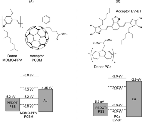 | ||
| Fig. 1 Chemical structures and associated energy level diagrams for the donor/acceptor materials used in this work: (A) MDMO-PPV:PCBM and (B) PCz:EV-BT. | ||
The photocurrent Jlight generated by a solar cell can be treated as the sum of a photogenerated current Jph due to the flux of incident photons, and a bias-induced current JVphoto due to the photovoltage Vphoto across the electrodes:14
| Jlight = Jph + JVphoto | (1) |
| Jlight(V) = Jph(V) + Jdark(V) | (2) |
| Jph(V) = Jlight(V) − Jdark(V) | (3) |
The conceptually simplest way to measure the Jph–V curve is to carry out sequential current–voltage sweeps in the dark and light and then calculate the difference. But, in practice, this yields an overestimate of the corrected photocurrent due to strong radiative heating when the device is illuminated by the light-source.14 To avoid this problem, we have developed a pulsed measurement scheme that ensures Jlight and Jdark are obtained at identical temperatures and so yields a reliable value of Jph (see Methods and ref. 14). In short, the applied bias is incremented in equal steps of height ΔV and width Δt; a white LED is used as the light-source and subjected to a square-wave modulation of frequency 1/Δt such that the device spends the first half of each voltage-step in the dark and the second half under illumination. Importantly, by selecting a time-step that is much shorter than the heating/cooling time of the device (Δt ≪ 10 ms), the dark- and light-currents can be measured at effectively the same temperature, thereby enabling a reliable measurement of the Jph–V curve to be obtained. All current–voltage measurements reported below were obtained using the pulsed scheme.
Results
(a) MDMO-PPV:PCBM
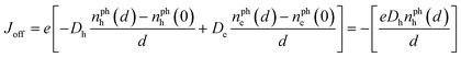
The first device investigated here was an ITO/PEDOT:PSS/MDMO-PPV:PCBM/Ag device (see the Methods section). Charge separation in MDMO-PPV:PCBM donor/acceptor blends occurs via an electron-transfer process from the −3 eV LUMO level of the light-harvesting MDMO-PPV to the −4.3 eV LUMO level of PCBM. The 1.3 eV energy offset is substantially greater than the ca. 0.5 eV offset usually considered necessary to achieve efficient exciton dissociation in organic semiconductor systems, suggesting that the spontaneous yield of free carriers should be high in this device.In Fig. 2, we show the Jdark–V, Jlight–V and Jph–V curves determined using the pulsed measurement scheme described above with an instantaneous illumination level of 90 mW cm−2. (The inset shows the spectral response curve under low intensity illumination.) The device has a short-circuit photocurrent ηSC of 11.4% and an open-circuit voltage VOC of 0.71 V at the quoted illumination level. The Jdark–V and Jlight–V curves are fairly standard in appearance and are similar to those reported elsewhere in the literature. The Jph–V curve, though, is more interesting since it is highly antisymmetric in appearance. The curve is reproduced in Fig. 3(A), where it has been divided into two zones to the left (L) and right (R) of a selected voltage that we refer to as the point of optimal symmetry (POS). To aid visualisation, the left-side data have been rotated 180° about the POS to generate a new curve (Lrot) that overlaps closely with the right-side data. The curve is almost perfectly symmetric in the range 0.3 < V < 1.3 V. The point of optimal symmetry – as its name suggests – is simply the bias that, after rotation, yields the optimal overlap between Lrot and R. The symmetry point occurs at a voltage of VPOS = 0.80 ± 0.01 V and a current of JPOS = −0.25 ± 0.14 mA cm−2. The slope of the Jph–V curve as a function of the applied bias is shown in Fig. 3(B). The slope is highest at the symmetry point and decreases monotonically either side – an observation that we will return to later.
 | ||
| Fig. 2 J dark–V, Jlight–V and Jph–V curves for an ITO/PEDOT:PSS/MDMO-PPV:PCBM/Ag device determined using the pulsed measurement scheme described in the Methods section with an instantaneous illumination level of 90 mW cm−2. The inset shows the spectral response curve under low intensity illumination. | ||
 | ||
| Fig. 3 (A) The Jph–V curve for the ITO/PEDOT:PSS/MDMO:PPV-PCBM/Ag device from Fig. 2. The curve has been divided into two parts to the left (L) and right (R) of a point of optimal symmetry (POS) at V = 0.80 V. The left-side curve has been rotated by 180° about the POS to create a new curve (Lrot) that overlaps closely with R, implying a high degree of symmetry in the current–voltage characteristics. The POS is the voltage that yields the best overlap between R and Lrot. (B) The slope of the Jph–V curve from Fig. 3(A) as a function of applied bias. The slope has a maximum at the POS and decreases monotonically at higher and lower voltages. | ||
The observed antisymmetry in the Jph–V characteristics – which in our experience is a virtually universal feature of BHJ devices – is evident only when care is taken to eliminate temperature differences between Jlight and Jdark. The antisymmetry can be rationalised by treating the active layer as a composite semiconductor, in which the HOMO and LUMO levels are derived from the donor and acceptor, respectively. In this approximation the device can be treated as a simple, single-layer solar cell, for which it can be shown:14
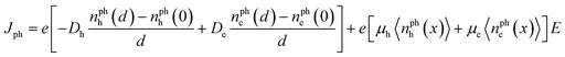 | (4) |
| Jph = Joff + σE | (5) |
 | (6) |
| σ = e[μh〈nphh(x)〉 + μe〈nphe(x)〉] | (7) |
Conceptually, we can classify three types of electrodes: non-selectiveelectrodes which allow ready extraction of both electrons and holes; self-selectiveelectrodes which give rise to preferential extraction of their own carrier type (holes to the anode and/or electrons to the cathode); and inversely-selectiveelectrodes which give rise to preferential extraction of their opposite carrier type (holes to the cathode and/or electrons to the anode). See ref. 14 for a discussion of potential causes of electrode selectivity. In the simplest case of non-selective electrodes, the electrons and holes are extracted into the external circuit as soon as they reach the electrodes, which depletes their concentrations. Hence, to a good approximation, we can write nphh(0) = nphh(d) = nphe(0) = nphe(d) = 0. In these circumstances, Joff = 0 and eqn (5) reduces to
| Jph = σE = e[μh〈nphh(x)〉 + μe〈nphe(x)〉]E | (8) |
The same general reasoning applies in the case of selective electrodes, except that the Jph–V curve is shifted downwards or upwards, depending on whether the electrodes are self-selective or inversely-selective. For instance, consider the case where the anode is non-selective and the cathode is self-selective. This leads to a situation in which nphe(0) = nphh(0) = nphe(d) = 0 due to rapid extraction but nphh(d) > 0. In this case, we obtain for Joff a non-zero negative value:
 | (9) |
The field-dependence of σ can be estimated experimentally by substituting into eqn (5)VBI = VPOS§ and Joff = JPOS. The latter identity is equivalent to assuming that Joff is constant across the entire measurement range, although strictly speaking this applies only in the central portion of the Jph–V curve where the curve is truly antisymmetric.¶ However, a general ‘feel’ for the likely shape of the σ(E) curve can be obtained by extending the range outwards. In agreement with the discussion above, the resultant curve – which is denoted ![[small sigma, Greek, circumflex]](https://www.rsc.org/images/entities/i_char_e111.gif) in Fig. 4 to emphasise the approximate nature of the calculation – is a positive, monotonically decreasing function of the electric field strength with a maximum at E = 0.
in Fig. 4 to emphasise the approximate nature of the calculation – is a positive, monotonically decreasing function of the electric field strength with a maximum at E = 0.
 | ||
| Fig. 4 The empirically determined field-dependence of σ for the ITO/PEDOT:PSS/ MDMO-PPV:PCBM/Ag device from Fig. 2 obtained using eqn (5) and the values of VPOS and JPOS from Fig. 3. | ||
(b) PCz:EV-BT
The second device investigated here was an ITO/PEDOT:PSS/PCz:EV-BT/Ca/Ag device (see the Methods section). EV-BT is the dominant light-harvester in PCz:EV-BT donor–acceptor blends so, unlike MDMO-PPV:PCBM, charge separation is due mainly to hole transfer from the −6.0 eV HOMO level of EV-BT to the −5.6 eV HOMO level of PCz. The 0.4 eV energy offset is smaller than the ca. 0.5 eV offset usually considered necessary to achieve efficient exciton dissociation in organic semiconductor systems, suggesting field-dependent carrier generation effects may be important in this materials system.In Fig. 5, we show the Jdark–V, Jlight–V and Jph–V curves determined using the pulsed measurement scheme with an instantaneous illumination level of 90 mW cm−2. (The inset shows the spectral response curve under low intensity illumination.) The device had a short-circuit quantum efficiency of 5.7% and an open-circuit voltage of 1.30 V at the quoted illumination level. The Jdark–V curve is qualitatively similar to that of the MDMO-PPV device discussed above. The Jlight–V curve, however, is quite different, exhibiting a number of unusual kinks (inflections) close to the open-circuit voltage. Similar kinks are evident in the Jph–V curve, implying that they are related in some way to the charge generation or extraction properties of the active layer.
 | ||
| Fig. 5 J dark–V, Jlight–V and Jph–V curves for an ITO/PEDOT:PSS/PCz:EV-BT/Ca/Ag device determined using the pulsed measurement scheme described in the Methods section with an instantaneous illumination level of 90 mW cm−2. Kinks are clearly evident in the Jlight–V and Jph–V curves. The inset shows the spectral response curve under low intensity illumination. | ||
The Jph–V curve, which is replicated in Fig. 6(A), has a roughly antisymmetric profile with a point of optimal symmetry at 1.62 ± 0.01 V.|| To aid visualisation the data have again been divided into two parts L and R, and the left-side data have been rotated by 180° to generate a new curve Lrot. Lrot and R show a very close correspondence from VPOS to 2.1 V, implying excellent symmetry in this range, but diverge somewhat at higher biases with R being substantially larger in magnitude. The current JPOS at the point of optimal symmetry has a small positive value of 0.12 ± 0.01 mA cm−2, consistent with at least one of the electrodes being (slightly) inversely-selective in nature. A positive offset-current has a deleterious effect on device efficiency since it yields a lower (less negative) photocurrent in the operating range 0 < V < Voc than would be observed in the case of non-selective electrodes.
 | ||
| Fig. 6 (A) The Jph–V curve for the ITO/PEDOT:PSS/PCz:EV-BT/Ca/Ag device from Fig. 5. The data have been divided into two parts to the left (L) and right (R) of a point of optimal symmetry (POS) at V = 1.62 V. The left-side data have been rotated by 180° about the POS to create a new curve (Lrot) that overlaps closely with R, implying a high degree of symmetry in the current–voltage characteristics. (B) The slope of the Jph–V curve from Fig. 6(A) as a function of applied bias. The slope has a minimum at the POS and peaks at biases of 1.29 and 2.07 V. | ||
Of particular interest in the current context are the three points of inflection in the Jph–V curve: one is located at the 1.62 V symmetry point where the slope has a local minimum; the others are located at 1.29 and 2.07 V where the slope has local maxima [Fig. 6(B)]. The inflection points are hard to rationalise in terms of the simple model set out above as can be seen from the following argument. Ignoring for a moment the offset-current Joff (which to a first approximation causes only a vertical displacement of the Jph–V curve and in any case is fairly close to zero for the PCz:EV-BT device), Jph is equal to the product of a supposedly monotonically decreasing even function σ(E) and the linear function E. Hence, Jph should exhibit a sub-linear dependence on E. In other words its slope should be largest at the built-in potential VBI (where E = 0) and decrease steadily towards zero with increasing field strength. This is just what we found for the MDMO-PPV:PCBM device [Fig. 3(B)]. However, it is most certainly not the case for the PCz:EV-BT device whose Jph–V curve exhibits a local minimum in the slope at the symmetry point [Fig. 6(B)].
Evidently the model presented above cannot account for the inflections in the Jph–V curve. If we assume that we can still treat the PCz:EV-BT device as a simple single-layer device, we conclude σ(E) is not in fact a monotonically decreasing function of the electric field (as expected from the simple field-sweeping argument proposed above) and must have a more complex functional form. By again assuming VBI = VPOS and Joff = JPOS, we can obtain an approximation (E) for the field dependence of the photoconductivity. The result, shown in Fig. 7, is a roughly even double-humped function of the electric field which decreases towards zero in the limit of high absolute field strength.
 | ||
| Fig. 7 The empirically determined field-dependence of σ for the ITO/PEDOT:PSS/ PCz:EV-BT/Ca/Ag device from Fig. 5 obtained using eqn (5) and the values of VPOS and JPOS from Fig. 6. | ||
In the central region of the curve, where the antisymmetry is ‘exact’, increases sharply with increasing field-strength. From eqn (7), this implies an increase in the density of photogenerated charge carriers and/or an increase in their mobilities with increasing field strength. Time-of-flight measurements on other photovoltaic blend systems indicate that the carrier mobilities typically show only a weak dependence on the electric field and in some cases can even decline with increasing field strength.18–20 Moreover, an analytical treatment of device operation (based on the assumption of negligible recombination) that we will present elsewhere indicates that the photoconductivity σ is independent of the carrier mobilities. Hence it is unlikely (although not impossible) that the sharp increase in the photoconductivity is due to an increase in the carrier mobilities. This leaves an increase in the average densities of photogenerated charge carriers, i.e. an increase in the free carrier yield, as the most probable reason for the super-linear field-dependence of σ in the low field regime.
We can reconcile the monotonically decreasing form of the photoconductivity in Fig. 4 with the double-humped form in Fig. 7 if we introduce a new function g(E) defined as the fraction of photogenerated excitons that dissociate into free electron–hole pairs under an electric field E. Eqn (5) then becomes
| Jph = [Joff-0 + σ0(E)E]g(E) | (10) |
| σ0(E) = e[μh〈nphh0(x,E)〉 + μe〈nphe0(x,E)〉] | (11) |
in Fig. 7.
Finally, in anticipation of the discussion in the next section, we note that differentiation of eqn (10) yields the following expression for the slope of the Jph–E curve
 | (12) |
 | (13) |
Discussion
Considerable insight into the consequences of field-dependent carrier generation can be obtained by applying the arguments outlined above to an imaginary ‘model’ device in which we are able to control the free carrier yield g(E) at will. We start by considering the ideal situation in which all photogenerated excitons dissociate spontaneously into free electron–hole pairs even when the internal field strength is zero, i.e. the yield g(E) = g0(E) is unity at all field strengths [Fig. 8(A)]. In accordance with the discussion above, the photoconductivity (under complete exciton dissociation) σ0(E) is assumed to be a monotonically decreasing function of the electric field E [Fig. 8(B)]. And, for simplicity, the offset-current Joff(E) is taken to be zero.†† The Jph–E curve [Fig. 8(C)] is given by eqn (5) and is self-evidently antisymmetric due to the respective even and odd symmetries of σ0(E) and E. | ||
Fig. 8 Schematic diagram explaining the effect of field-dependent carrier generation on the current–voltage characteristics, assuming an offset-current of zero. (A) The ‘ideal’ situation in which the free carrier yield g0(E) is 100% at all field strengths. (B) The (arbitrary unit) photoconductivity σ0(E) corresponding to case (A); σ0(E) is an even monotonically decreasing function of the electric field. (C) The (arbitrary unit) corrected photocurrent Jph(E) = σ0(E)E corresponding to case (A). (D) The free carrier yield g1(E) for an ‘intermediate’ situation in which the carrier yield increases monotonically from 50% at E = 0 to 100% as E![[hair space]](https://www.rsc.org/images/entities/char_200a.gif) →∞. (E) The photoconductivity σ1(E) = σ0(E)g1(E) corresponding to case (D). (F) The corrected photocurrent Jph(E) = σ1(E)E = σ0(E)g1(E)E, corresponding to case (D). (G) The free carrier yield g2(E) for an ‘extreme’ case in which the yield increases monotonically from zero at E = 0 to 100% as E→∞. (H) and (I) show the photoconductivity and corrected photocurrent corresponding to case (G). →∞. (E) The photoconductivity σ1(E) = σ0(E)g1(E) corresponding to case (D). (F) The corrected photocurrent Jph(E) = σ1(E)E = σ0(E)g1(E)E, corresponding to case (D). (G) The free carrier yield g2(E) for an ‘extreme’ case in which the yield increases monotonically from zero at E = 0 to 100% as E→∞. (H) and (I) show the photoconductivity and corrected photocurrent corresponding to case (G). | ||
We now consider the effect of introducing a simple field-dependence into the free carrier yield, assuming no other changes to the device. We consider an ‘intermediate’ situation in which the yield g1(E) is 50% at zero field rising monotonically to 100% at high field strengths [Fig. 8(D)]. The photoconductivity σ1 is obtained by multiplying σ0(E) by g1(E) [see eqn (10)], which yields a curve with the expected double-humped functional form [Fig. 8(E)]. The Jph–E curve obtained from eqn (5) retains an antisymmetric appearance but, as expected, develops three points of inflection [Fig. 8(F)]. In accordance with eqn (13), the slope at the central point of inflection is reduced by a factor of two due to the two-fold reduction in g(0).
The same general behaviour is observed when the yield g2(E) is 0% at zero field rising monotonically to 100% at high field strengths [Fig. 8(G)]. Again, σ2 has a double-humped appearance, although it now obviously equals zero when E = 0 [Fig. 8(H)]. The antisymmetric Jph–E curve again has the expected three points of inflection, and the slope at the central inflection is now zero in agreement with eqn (13) [Fig. 8(I)].
In Fig. 9, we overlay the three Jph–V curves corresponding to the illustrative data in Fig. 8. The curves all pass through zero at V = VBI (due to the assumption of a zero-valued offset-current) albeit with progressively diminishing slopes as g(0) tends towards zero. The inflections caused by the field-dependent free carrier yield are (unsurprisingly) detrimental to device performance since, geometrically speaking, they cause the Jph–V curve (and hence the Jlight–V curve) to bend inwards to the origin, lowering the fill-factor and the short-circuit current. The effect is most pronounced in the third case since the free carrier density falls to zero at V = VBI, causing a complete flattening of the Jph–V curve.‡‡
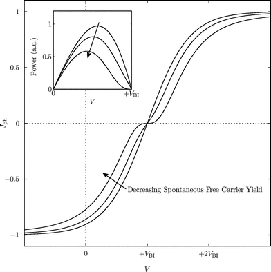 | ||
| Fig. 9 Schematic diagram showing the overlaid Jph–V curves for the three cases considered in Fig. 8. The three curves intersect at the built-in potential where the current falls to zero due to the assumed zero offset-current. The curves bend inwards towards the origin as the spontaneous yield of free carriers diminishes. The inset shows the voltage-dependence of the power curve for the three situations. There is a progressive reduction in the peak power as the yield diminishes. | ||
The intermediate case in Fig. 9 is similar to the situation observed experimentally in Fig. 6(A) where the slope has a non-zero value at the point of optimal symmetry. One possible explanation for the non-zero slope is a contribution to the photocurrent from excitons generated in the less-strongly absorbing PCz phase. These excitons dissociate via an electron-transfer process, for which the ca. 1 eV LUMO–LUMO offset is large enough to ensure efficient spontaneous free carrier generation even in the absence of an electric field. Returning to the excitons harvested in the EV-BT layer, the locations of the outer points of inflection provide some indication of the field needed to initiate significant free carrier generation – in this case ca. 8 × 10⁶ V m−1. Importantly, it should be possible to lower this value by functionalising the PCz in such a way as to raise its HOMO level by a few tenths of an electron volt (thereby ensuring that the electron and hole gain sufficient kinetic energy to overcome their residual attraction).§§
Conclusion
We have considered BHJ devices based on two materials systems, MDMO-PPV:PCBM and PCz:EV-BT, in which the relevant frontier orbitals are offset by 1.3 and 0.4 eV, respectively. The corrected current–voltage response of the devices can be rationalised in terms of a simple model in which the devices are treated as a single layer of composite semiconductor sandwiched between two electrodes. The Jph–V response of MDMO-PPV:PCBM devices is consistent with a model in which all – or at least a fixed field-independent fraction of – photogenerated excitons dissociate spontaneously into free electron–hole pairs. In such a model, the Jph–V curve has an antisymmetric profile centred about the built-in potential, and its slope decreases monotonically towards zero with increasing field strength. The Jph–V response of PCz:EV-BT devices by contrast is consistent with a model in which the fraction g(E) of photogenerated excitons that dissociate into free electron–hole pairs is a monotonically increasing function of the electric field strength |E|. In this case, three points of inflection appear in the Jph–V characteristics. The central point of inflection coincides with the built-in potential and corresponds to a minimum in the slope. The outer points of inflection – which are distributed roughly symmetrically about the built-in potential – correspond to maxima in the slope. The separation of the inner and outer points of inflection suggests that a field strength of approximately 8 × 10⁶ V m−1 is required to achieve appreciable free carrier generation.The occurrence of field-dependent carrier generation in PCz:EV-BT devices is consistent with the relatively small ca. 0.4 eV energy offset between the HOMO levels of PCz and EV-BT. The spatially-separated electron and hole are unlikely to gain sufficient kinetic energy in the charge-transfer process to overcome the binding energy of the charge-transfer exciton so-formed, and consequently they have a high probability of recombining. In the presence of a sufficiently strong electric field, the electron and hole are pulled in opposite directions, lowering their recombination probability and hence improving the yield of free carriers.
Methods
The PCz:EV-BT bulk heterojunction solar cell was fabricated by spin-coating on to an indium tin oxide (ITO) coated glass substrate a ca. 30 nm layer of poly(3,4-ethylenedioxy-thiophene):poly(styrenesulfonate) (PEDOT:PSS) (Baytron VP Al 4083) at 1500 rpm from aqueous solution. The sample was heated in air at 140 °C for 20 min to drive off excess water, and was then transferred to a dry nitrogen atmosphere. All subsequent fabrication steps and measurements were carried out under dry nitrogen. The device was not exposed to air at any point after drying the PEDOT:PSS layer. A PCz:EV-BT blend was spin-coated at 2000 rpm on top of the dried PEDOT:PSS layer from a 10 mg ml−1chloroform solution with 30 wt% PCz. The PCz:EV-BT film was then annealed for 10 min at 80 °C and was completed by sequentially evaporating a Ca cathode and a protective capping layer of Agvia a shadow mask under a pressure of ca. 10−5 mbar. The active area of the device – determined by the spatial overlap of the patterned anode and cathode – was approximately 12 mm2. The PCz was kindly provided by Professors Klaus Müllen and Martin Baumgarten and the EV-BT was synthesised in IMRE.The MDMO-PPV:PCBM device was fabricated by spin-coating at 1500 rpm on to an ITO/PEDOT:PSS substrate (prepared in the manner described above) a composite layer of MDMO-PPV (20 wt%, Sigma-Aldrich) and PCBM (American Dye Source) from a 17.5 mg ml−1 solution in chlorobenzene. The sample was heated on a hotplate at 60 °C for 10 min to remove excess solvent. A silver cathode was deposited by thermal evaporation through a shadow mask under a pressure of ca. 10−5 mbar, giving a device area of approximately 13 mm2.
Spectral response curves were determined using the monochromated and mechanically-chopped (237 Hz) output of a xenon lamp. The modulated photocurrent was converted to a voltage signal by means of a 50 Ω resistor – to ensure near short-circuit conditions – and detected by a Stanford Research SR830 lock-in amplifier. The intensity of the incident monochromatic light was determined using a calibrated Si photodiode.
To obtain the Jph–V characteristics, a previously-reported pulsed measurement procedure was used, which ensures that Jlight and Jdark are obtained at the same temperature despite strong radiative heating by the light-source. In short, the voltage was incremented in equal steps of width Δt (200 μs) and height ΔV (20 mV for MDMO-PPV:PCBM, and 50 mV for PCz:EV-BT). A white LED light-source was subjected to a square-wave modulation voltage of frequency 1/Δt such that the device spent the first half of each voltage-step in the dark and the second half under illumination. The incident light intensity was measured with an Ophir Nova II thermopile power meter. The time-varying current through the solar cell was converted to a voltage signal using a gain 100 Ω trans-impedance amplifier (with low input impedance) and supplied as an input to a National Instruments PCI-6251 data acquisition card. Importantly, by selecting a time-step that is much shorter than the heating/cooling time of the device (Δt ≪ 10 ms), the dark- and light-currents at each voltage are obtained at effectively the same temperature, thereby enabling a reliable estimate of Jph to be made. In this way, one avoids the systematic errors that are usually incurred when the Jph–V characteristics are determined from successive current–voltage sweeps in the light and dark (as is usual practice in the literature). The slopes of the Jph–V curve in Fig. 3(B) and Fig. 6(B) were determined by carrying out least-squares spline approximations to the raw data prior to numerical differentiation. By eye, the spline approximants were indistinguishable from the original data when superimposed on the data in Fig. 3(A) and 6(A).
Acknowledgements
The authors are grateful to Professors Klaus Müllen and Martin Baumgarten for the provision of the PCz used in this work. The authors also acknowledge support from the UK Engineering and Physical Sciences Research Council (GR/T26559/01) and the Singapore Agency for Science, Technology and Research (A*STAR) under the A*STAR-Imperial Partnership.References
- T. L. Benanti and D. Venkataraman, Photosynth. Res., 2006, 87, 73–81 CrossRef CAS.
- J. Peet, J. Y. Kim, N. E. Coates, W. L. Ma, D. Moses, A. J. Heeger and G. C. Bazan, Nat. Mater., 2007, 6, 497–500 CrossRef CAS.
- J. J. M. Halls, J. Cornil, D. A. dos Santos, R. Silbey, D. H. Hwang, A. B. Holmes, J. L. Bredas and R. H. Friend, Phys. Rev. B, 1999, 60, 5721–5727 CrossRef CAS.
- M. A. Loi, S. Toffanin, M. Muccini, M. Forster, U. Scherf and M. Scharber, Adv. Funct. Mater., 2007, 17, 2111–2116 CrossRef CAS.
- L. J. A. Koster, V. D. Mihailetchi and P. W. M. Blom, Appl. Phys. Lett., 2006, 88.
- A. C. Morteani, P. Sreearunothai, L. M. Herz, R. H. Friend and C. Silva, Phys. Rev. Lett., 2004, 92.
- C. L. Braun, J. Chem. Phys., 1984, 80, 4157–4161 CrossRef CAS.
- H. Tamura, E. R. Bittner and I. Burghardt, J. Chem. Phys., 2007, 126.
- H. Tamura, J. G. S. Ramon, E. R. Bittner and I. Burghardt, J. Phys. Chem. B, 2008, 112, 495–506 CrossRef CAS.
- S. E. Shaheen, C. J. Brabec, N. S. Sariciftci, F. Padinger, T. Fromherz and J. C. Hummelen, Appl. Phys. Lett., 2001, 78, 841–843 CrossRef CAS.
- C. Lungenschmied, G. Dennler, H. Neugebauer, N. S. Sariciftci and E. Ehrenfreund, Appl. Phys. Lett., 2006, 89, 3.
- P. W. M. Blom, V. D. Mihailetchi, L. J. A. Koster and D. E. Markov, Adv. Mater., 2007, 19, 1551–1566 CrossRef CAS.
- Z. E. Ooi, T. L. Tam, R. Y. C. Shin, Z. K. Chen, T. Kietzke, A. Sellinger, M. Baumgarten, K. Mullen and J. C. deMello, manuscript in preparation.
- Z. E. Ooi, R. Jin, J. Huang, Y. F. Loo, A. Sellinger and J. C. deMello, J. Mater. Chem., 2008, 18, 1644–1651 RSC.
- D. H. Dunlap, Phys. Rev. B, 1995, 52, 939–954 CrossRef CAS.
- I. H. Campbell, T. W. Hagler, D. L. Smith and J. P. Ferraris, Phys. Rev. Lett., 1996, 76, 1900–1903 CrossRef CAS.
- P. A. Lane, P. J. Brewer, J. S. Huang, D. D. C. Bradley and J. C. deMello, Phys. Rev. B, 2006, 74, 7.
- M. Vanderauweraer, F. C. Deschryver and P. Borsenberger, Chem. Phys., 1994, 186, 409–433 CrossRef CAS.
- R. H. Young, J. Chem. Phys., 1995, 103, 6749–6767 CrossRef CAS.
- J. S. Huang, G. Li and Y. Yang, Appl. Phys. Lett., 2005, 87.
Footnotes |
| † Note, the shape of the Jph–V curves is found to be invariant with light intensity over a broad range of intensities, retaining the same symmetric appearance from low intensities up to (and beyond) one sun illumination. This shape invariance indicates that the electric field must be constant throughout the bulk of the device since this is certainly the case at sufficiently low intensities, and any changes to the electric field profile at higher intensities would lead to changes in the shape of the Jph–V response. The symmetry of the Jph–V characteristics is further evidence that the density of charge carriers inside the device is too low to modify the electric field profile (since appreciable differences would otherwise be expected between forward and reverse oriented fields). Hence the internal field strength is given by: E = (V − VBI)/d. |
| ‡ Asymmetry in the generation profile (caused by the one-sided illumination through the glass substrate and potential interference effects) introduces a slight non-evenness into the field-dependence, but device simulations to be reported elsewhere show this to be a very weak effect. |
| § The observed value VPOS = 0.80 V is reasonably consistent with the anode and cathode work functions of −5.2 and −4.35 eV which, in a simple model, would be expected to yield a built-in potential of ca. 0.85 V. |
| ¶ The loss of antisymmetry outside this range is attributable to Joff having a non-constant value which, from eqn (5), causes the Jph–E curve to deviate in shape from the antisymmetric σEversusE curve. The field-dependence of Joff will be addressed in a future manuscript. |
| || The Fermi level of the Ca cathode is expected to pin to the −3.6 eV LUMO level of the acceptor. Hence, the value VPOS = 1.6 V is consistent with the 1.6 eV energy difference between the −5.2 eV work function of PEDOT:PSS and the pinned −3.6 eV Fermi level of Ca. |
| ** At moderate light levels Jph varies linearly with the incident light level, which implies that Jph(E), Joff(E) and σ(E) are all proportional to the exciton generation rate, and hence also to g(E). This is the experimental justification for eqn (10). |
| †† A non-zero offset-current will disrupt the antisymmetry of the Jph–V curve because, from eqn (10), it introduces an additional even-symmetry term Joff-0g(E). However if the offset-current is small (as is true in the case of the PCz:EV-BT device), this effect will be small and the antisymmetry will be retained to a good approximation. |
| ‡‡ This bending of the Jph–V and Jlight–V curves provides one explanation for the occurrence of <0.25 fill-factors occasionally reported in the literature. Considerable insight into the exciton dissociation process might be gained by studying how the critical field strength varies with the HOMO energy of PCz and this is something we hope to address in a future study. |
| §§ In principle it should be possible to raise the HOMO level to −5.2 eV (which is the work function of PEDOT:PSS) without risking any reduction in the built-in field. |
| This journal is © The Royal Society of Chemistry 2008 |