Patterning micron-sized features in a cross-linked poly(acrylic acid) film by a wet etching process†
Adam
Winkleman
,
Raquel
Perez-Castillejos
,
Michal
Lahav
,
Max
Narovlyansky
,
Leonard N. J.
Rodriguez
and
George M.
Whitesides
*
Department of Chemistry and Chemical Biology, Harvard University, 12 Oxford St., Cambridge, MA 02138. E-mail: gwhitesides@gmwgroup.harvard.edu; Fax: +1 (617) 495-9857; Tel: +1 (617) 495-9430
First published on 23rd November 2006
Abstract
This paper describes a photolithographic method to create sub-micron-scale patterns of cation-cross-linked poly(acrylic acid) (CCL-PAA). PAA can be cross-linked with a wide range of metal cations—including, but not limited to, Ag+, Ca2+, Pd2+, Al3+, La3+, and Ti4+. Upon patterning a positive photoresist (diazonaphthoquinone-novolac resin) on a film of CCL-PAA, the exposed regions of CCL-PAA were etched by either an aqueous NaOH or EDTA solution. The initial cross-linking cation could be exchanged for a second cation that could not be patterned photolithographically. We used these patterned films of CCL-PAA i) to host and template the reduction of metallic cations to metallic nanoparticles, and ii) to fabricate porous, low-k dielectric substrates.
Introduction
This paper describes a simple photolithographic method to create sub-micron-scale patterns of cation-cross-linked poly(acrylic acid) (CCL-PAA) in which the cross-linking cations can be exchanged for other cations. We processed these films to generate patterned metallic nanoparticles and low-k dielectric materials. A patterned layer of positive photoresist (diazonaphthoquinone-novolac resin) blocked selectively the aqueous etching of only the unexposed regions of an underlying layer of CCL-PAA; acetone dissolved the masking photoresist without affecting the CCL-PAA. After patterning the CCL-PAA film, we could exchange the metal cation originally used for cross-linking with another cation—either a different metal cation (e.g., Pd2+) or a cationic organic molecule (e.g., 3,6-diaminoacridine hydrochloride (DAH))—by soaking the film in a concentrated solution of the second cation. Reduction of a CCL-PAA film containing Pd2+ or Ag+ yielded patterns of metallic nanoparticles embedded within the film. Calcination or ozonation of an Al3+-cross-linked PAA film generated a patterned, porous oxide film with the characteristics of a low-k dielectric. The CCL-PAA matrix, in which we successfully incorporated 17 different metal cations, offers a new platform for positioning and fabricating nanomaterials with sub-micron spatial control. The use of photolithographic techniques should facilitate the incorporation of these new materials into existing technologies including those for microelectronics.The ability to pattern thin polymer films on substrates is central to microelectronics,1,2 optics,3,4 MEMS,5 and biochemistry.6,7 There are several ways to pattern polymers, including e-beam writing8 and laser ablation,9,10 (which are non-parallel and inherently slow), and various techniques based on soft lithography.1,11–19 The patterning of thin polymer films by photolithography has typically been limited to polymer photoresists,20,21 but photoresists, unlike PAA, cannot serve as matrices for further organic reactions (because they dissolve in organic solvents) or as matrices for metal ions. Husemann et al. demonstrated the use of a photoresist overlayer to template an underlying polymer film; a poly(t-butyl acrylate) polymer brush was selectively converted into PAA by photolithography.22
Thin-film, low-k dielectric substrates are polymers or inorganic oxides having dielectric constants (k) lower than bulk silicon dioxide (k ≈ 4).23–26 Capacitance depends on the dielectric constant, so low-k dielectric materials are desirable because they reduce the capacitance between wires and allow increased operating frequencies in microelectronic devices.24 There is great interest in generating porous dielectrics because of their reduced effective dielectric constant as compared to bulk materials.23 A common technique for fabricating low-k materials is spinning a solution or suspension (a sol) of the dielectric, followed either by solvent evaporation (i.e., xerogels),27 or by supercritical drying of the gel (i.e., aerogels).28 Chemical vapor deposition (CVD)29 is also used to generate thin silica oxides with high porosity. Sacrificial organic macromolecules—a porogen (e.g., dendridic polymers)—have templated and controlled the porosity of the metal oxides—most notably silicates—in order to fabricate materials with low dielectric constants.30–32 The materials produced by both methods are often mechanically very fragile, and post-processing steps—including patterning of the low-k dielectric films—are technically difficult. The procedures presented here allow for patterning of the CCL-PAA prior to converting it to a low-k dielectric film by calcination or ozonation of the organic matrix.
Results and discussion
Formation of the CCL-PAA film
Fig. 1 illustrates the process we used to pattern CCL-PAA films. We began by spin-coating a layer of PAA (3.5% w/v in water, pH 2.5) onto either a silicon or glass substrate that we had treated with an air plasma, and baking this layer at 150 °C for 15 minutes. We then spun a second layer of PAA (pH 7.2) onto the initial layer and baked at 150 °C for 2 minutes to remove the water. Successive deposition of two layers of PAA was necessary in order to ensure good adhesion of the neutral layer to the substrate; the carboxyl groups in PAA (pH 2.5) react at 150 °C with surface hydroxyl groups and form ester bonds.33 After the two layers of PAA were spun-cast and baked, we immersed the substrate in an aqueous solution containing a metal salt (typically 1 M) for 1 minute. | ||
| Fig. 1 A schematic representation for the process used to fabricate a patterned thin film of CCL-PAA using photolithography and wet-etching. After spin-casting and baking an adhesion layer of PAA (pH 2.5) onto a glass or silicon substrate, a second layer of PAA (pH 7.2) was spun-cast and cross-linked with an aqueous 1 M salt solution (e.g., CaCl2 (pH 6.8) or Al2(SO4)3 (pH ≈ 6.5)). A positive photoresist (a diazonaphthoquinone-novolac resin) was spun onto the CCL-PAA film and exposed to UV irradiation through a photomask. The exposed photoresist was removed by etching with a 0.7 M solution of NaOH. For some cations (e.g., Al3+ or Ca2+), the alkaline etchant dissolved both the exposed photoresist and the CCL-PAA directly beneath it. If the etchant could not uncross-link and dissolve the CCL-PAA—as it could not for La3+, Ho3+, or Ag+—a second aqueous solution containing 0.5 M EDTA was necessary to remove the CCL-PAA film. The unexposed photoresist was removed with acetone. This process yielded a patterned CCL-PAA structure on the substrate. Post-patterning processes permit the exchange of cross-linking ions as well as the fabrication of low-k dielectric substrates. | ||
We demonstrated experimentally that many metal cations—including alkaline earth metals, transition metals, and lanthanides—cross-link films of PAA. Table 1 lists these cations—and those that failed to cross-link the film—by atomic number. In order for a metal cation to cross-link a PAA film, at least two of the ligands in the inner coordination sphere of the metal cation must be replaced by carboxylate groups from PAA. We found four types of metal salts that failed to cross-link a PAA film: i) salts containing strongly-complexed metal cations, such as AuCl3, PdCl42−, and Fe(CN)63−, in which the inner-sphere ligands (Cl− or CN−) are tightly bound thermodynamically (Ka > 1010 M−1);34 ii) salts containing small, highly-charged metal cations that are strongly solvated by water or hydroxide, such as Mg2+ or B3+ (e.g., B(OH)3);35 iii) salts containing metal cations that are kinetically inert to inner-sphere ligand substitution, such as Cr3+ (the rate constant for substitution of an inner-sphere water molecule in Cr3+ (aq) is ∼10−6 s−1;)35 iv) salts containing metal cations for which the inner-sphere association with carboxylate ligands in water is thermodynamically unfavorable, such as Na+, K+, and Cs+ (the binding of a single acetate ligand to these cations in water is thermodynamically unfavorable, Ka < 1 M−1;34 the binding of two or more acetate ligands to these cations would be even more unfavorable.)
| Cross-linking | Non-cross-linking |
|---|---|
| a Films of PAA on a silicon wafer were immersed in either a 1 M or a saturated solution of each metal salt for 1 minute. The films were subsequently rinsed with water (pH ≈ 7) and dried with a stream of N2. Successfully cross-linked PAA films remained intact on the wafer; unsuccessful films dissolved. | |
| Al2(NO)3 | B(OH)3 |
| CaCl2 | NaCl |
| TiBr4 | NaOH |
| TiI4 | MgSO4 |
| MnCl2 | KCl |
| Fe(NO3)3 | TiF4 |
| FeCl2 | CrCl3 |
| NiSO4 | K4Fe(CN)6 |
| NiCl2 | K3Fe(CN)6 |
| Cu(OAc)2 | NaPdCl4 |
| ZnCl2 | CsCl |
| Zn(OAc)2 | AuCl3 |
| ZrCl4 | NaAuCl4 |
| ZrO(NO3)2 | Na3AuCl4 |
| Pd(SO4) | UO2SO4 |
| AgNO3 | |
| BaS | |
| BaCl2 | |
| La(NO3)3 | |
| GdCl3 | |
| Ho(NO3)3 | |
| Pb(OAc)2 | |
| UO2(OAc)2 | |
Patterning
We spun-cast a layer of positive photoresist (a diazonaphthoquinone-novolac resin) onto the CCL-PAA film. CCL-PAA is insoluble in organic solvents and is not affected by spin-casting or patterning of the photoresist. The thickness of the photoresist film was ∼1.5 microns for the larger features (>10 microns), and ∼500 nm for the smaller features (<1 micron). We exposed the photoresist to UV light through an appropriate photomask (either a transparency mask36 or a chrome mask) using a mask aligner. After UV exposure, we developed the photoresist and the CCL-PAA films using wet-etching. PAA films cross-linked with either Al3+ (Al2(SO4)3·12H2O) or Ca2+ (CaCl2) could be etched completely by exposing them to a commercial photoresist developer (typically a solution of 0.7 M NaOH) for 4–10 seconds at 20 °C. It was also possible to use a commercial developer containing aqueous solutions of 0.26 M tetramethylammonium hydroxide (TMAH) for 30–45 seconds.This developer alone did not etch films cross-linked with Ag+ (AgNO3), Ho3+ (Ho(NO3)3), La3+ (La(NO3)3), or Pd2+ (PdSO4). Exposure of the CCL-PAA/Ag+ film to the developer yielded a surface with a precipitate in the etched regions of the polymer. This precipitate may be insoluble Ag2O, but we have not determined its composition. For CCL-PAA/Ho3+ films, the rate of etching the polymer film was sufficiently slow that the photoresist was completely removed by the developer before the polymer film was properly etched (Supplemental Figure S1†). The CCL-PAA/La3+ film showed no signs of etching even after 10 minutes in the 0.7 M NaOH solution, while the CCL-PAA/Pd2+ films etched more rapidly than the photoresist, and thus were over-etched (Supplemental Figure S1†). We could not find conditions that yielded well-defined patterns in the CCL-PAA/Pd2+ film.
For those CCL-PAA films that could not be etched by the 0.7 M NaOH solution, an additional step was required. After removing the photoresist from the regions exposed to UV light with the developer, the samples were immersed in an aqueous solution containing 0.5 M EDTA (pH 8.5); this solution etched the areas of the CCL-PAA film exposed through the windows opened in the photoresist. The use of a competitive and stronger chelator than the carboxylates in the PAA extracted the cross-linking metal cations, and yielded water-soluble, uncross-linked PAA. The combined use of developer and EDTA solution successfully etched the CCL-PAA/Ho3+ and CCL-PAA/La3+ films. The aqueous EDTA solution also removed the precipitate from the Ag+ films, and yielded a clean pattern of well-defined features.37
Using optimized conditions for the specific metal cation, the etchant slightly over-etched the CCL-PAA film, in general. AFM showed that the differences between 22-µm-wide lines in the photomask and the features in the CCL-PAA films were <1 µm. The degree of over-etching did not depend on the cross-linking cation: similar results were measured for CCL-PAA cross-linked with Ag+, Ca2+, Al3+, Ho3+ and La3+.
Since the patterning in this technique is defined only by a photomask and photolithography, a wide range of features, both continuous and discontinuous, are possible (Fig. 2). We have fabricated arrays of CCL-PAA square posts (Fig. 2A) as well as square wells in a continuous CCL-PAA film (Fig. 2B), all with sides 100 µm in length. We have also fabricated posts and wells in other geometries such as triangles, circles, and pentagons with similar feature sizes. We have demonstrated the ability to fabricate concentric rings of CCL-PAA with constant width and increasing spacing between the lines (Fig. 2C), or (by using the inverse photomask) increasing line-width and a constant spacing between the lines (Fig. 2D). The edge roughness for all of these structures fabricated from photoplotted photomasks was ∼1 µm, the reported roughness of this printing technology36 (Supplemental Figure S2†).
 | ||
| Fig. 2 A series of optical and AFM images illustrating the resolution and range of the geometric patterns that we fabricated. We prepared films with Al3+ and Ca2+ as the cross-linking cations. Figures B, D, E, F, G and H show films that were cross-linked with Al3+ cations and figures A and C those that were cross-linked with Ca2+. A) A discontinuous pattern of 100 micron square posts of CCL-PAA. B) The inverse of (A) illustrating a continuous film of CCL-PAA with a pattern of square wells (100 microns wide). C and D) Two sets of concentric rings of CCL-PAA in which (C) the CCL-PAA line-width (20 microns) remained constant or (D) the space between rings remained constant. The insets in figures A, B, and C show a magnified region illustrating the well-defined edges. (E) An optical and (F) an AFM image of a series of 1 µm lines spaced by 1 µm. G) An AFM image of ∼500 nm lines spaced by ∼500 nm representing the lower limit we have demonstrated for the resolution of this technique. H) A fluorescent image of a CCL-PAA/Al3+ film cross-linked in the presence of rhodamine B (RhoB). | ||
The current minimum line width and line spacing that we have achieved with this technique is ∼500 nm using a chrome mask (Fig. 2G). To prevent over-etching of the 500 nm CCL-PAA/Al3+ features, we diluted the developer to a 0.47 M NaOH solution and etched for 3 seconds. The edge roughness of these features patterned from chrome masks is <70 nm, a size on the order of the resolution of the mask (Supplemental Figure S2†). To obtain features with lateral dimensions smaller than 500 nm, we would need to use more complex photolithographic techniques, and to re-optimize the etching process. The photoresist we used for this process is ∼500 nm thick and obtaining features with aspect ratios larger than 1 is difficult. Also, the CCL-PAA film is amorphous; thus the etching should be isotropic and lead to slight undercutting of the photoresist and over-etching of the CCL-PAA. Since the CCL-PAA films are ∼300 nm thick, this isotropic etching becomes more problematic when the lateral dimensions approach that of the film thickness.
Films that were cross-linked in the presence of an additional, non-interacting molecule retained these molecules during the etching process. A CCL-PAA/Al3+ film containing a dye (either fluorescein or rhodamine B) fluoresced after patterning. The fluorescence was only observed in the regions where the polymer film remained (Fig. 2H). (We took care to minimize the exposure of these samples to ambient light to prevent photobleaching.) We observed no fluorescence in CCL-PAA/Al3+ films in the absence of a dye.
Post-patterning modifications and applications
Soaking either CCL-PAA/Al3+ or CCL-PAA/Ca2+ in a concentrated aqueous solution (typically 1 M) containing a different metal cation (e.g., Pd2+ and Ag+) resulted in ion exchange after 30 minutes. Since we could not successfully form a patterned CCL-PAA with Pd2+, the only method to create a CCL-PAA/Pd2+ film was ion exchange. We also exchanged the Al3+ cation in a CCL-PAA/Al3+ film on a glass substrate with a cationic organic dye, DAH. (We allowed the polymer film (∼5 cm2) to soak for 1 hour in 10 mL of an aqueous, saturated solution of the dye before rinsing and drying the film.) The resulting polymer film was translucent under white light and highly fluorescent when excited (Fig. 3A). The edge roughness remains similar after exchange (Supplemental Figure S2D†). After soaking the fluorescent CCL-PAA/DAH overnight in an aqueous 100 mL solution of 1 M Al2(SO4)3 in the dark, the CCL-PAA film remained insoluble, but the film was no longer fluorescent. This observation indicates that the cation exchange in these films is reversible. | ||
| Fig. 3 Optical images obtained after exchanging the original cross-linking cation for another cation. A) A fluorescent image (λex = 470–490 nm, λem > 515 nm) of a CCL-PAA/DAH film in which 100 micron-wide squares were etched away. B) An array of 200 micron diameter circles of PAA after exchanging with Ag+ cations and photoreduction with a UV lamp. C) A CCL-PAA film patterned into an array of lines of different widths with a constant spacing (20 microns). The Pd2+ ions replaced the Al3+ and reduced to Pd0 upon exposure to an aqueous solution of 0.1 M borane dimethylamine complex (BDC) containing 1 M CaCl2. | ||
The cations present in the CCL-PAA film are accessible for further chemical reactions. We tested the CCL-PAA/Ag+ and CCL-PAA/Pd2+ films for reduction of the metal cation. Exposure of the CCL-PAA/Ag+ film to UV light for 20 minutes yielded a brown film (Fig. 3B). (This procedure is a common method for the photoreduction of silver cations to silver nanoparticles.)38 We confirmed the presence of nanoparticles using a TEM (Supplemental Figure S3†); the average size of a particle was 3 nm. After photoreduction, the film retained its integrity and insolubility in both water and an aqueous solution of 1 M NaOH. A CCL-PAA/Al3+ film exposed to UV light for 20 minutes was soluble in 1 M NaOH. We hypothesize that the photoreduction of Ag+ created radicals in the PAA polymer (due to an excited state silver ion abstracting a hydrogen atom from the polymer); and these radicals caused the polymer to cross-link;39 this cross-linking made the remaining CCL-PAA/Ag+ insoluble, and thus resistant to etching.
We exposed a CCL-PAA/Pd2+ film to a reducing solution containing 0.1 M borane dimethylamine complex (BDC) and 1 M CaCl2 in water (pH ≈ 8) for 1 minute (Fig. 3C). During the reduction, the color of the PAA film changed to a dark grey, and gas bubbles evolved at its surface. In addition to BDC, the solution had to contain a cation (here Ca2+) that was able to cross-link the chains, and was not reduced by the BDC, in order to keep the CCL-PAA cross-linked: in the absence of Ca2+, the CCL-PAA/Pd2+ film delaminated, and partially dissolved. We concluded that the BDC reduced most of the Pd2+ cations, and thus reduced or eliminated the cross-links in the PAA film. We believe that the Ca2+ cations in the solution replaced the Pd2+ cations that became Pd(0) colloidal particles to maintain the cross-linking of the polymer film (eqn (1)). In the presence of Ca2+ cations, we observed that the polymer film that remained on the substrate was insoluble in water after reduction of Pd2+.
 | (1) |
Low-k dielectric films
For fabricating patterned low-k dielectric films, the CCL-PAA/Al3+ films were either calcined at 750 °C for 4 hours in air or treated by UV/O3 for 3 hours to remove the polymer film: these oxidations yielded an insulating, inorganic, patterned film (Fig. 4A and B). We used a furnace at a temperature of 750 °C to ensure removal of all the organic polymer and to convert all the mobile cross-linking cations into an inorganic ceramic. The presence of mobile cations would increase the dielectric constant by increasing the polarizability of the material; mobile cations can also degrade the electrical performance by diffusing to the interfacial region. The thickness of the film before decomposition of the polymer was ∼300 nm; the final thickness of the residual metal oxide was 21–27 nm with an average thickness of ∼23 nm for the calcined film, and 46–53 nm with an average thickness of ∼49 nm for the ozonized film, as determined by both profilometry and AFM. The planar patterned geometry and edge roughness in the CCL-PAA after calcination and ozonation remained similar to that of the original CCL-PAA film (Supplemental Figure S2E†). The SEM images of the Al3+-containing structures show a rough, porous surface (Fig. 4C and D). A significant amount of charging of the surface occurred from the electron beam irradiation during the SEM imaging, as is expected for a dielectric material. A TEM image of the calcined film reveals that the grain size is between 2–5 nm and the porosity is of a similar size-scale (Fig. 4E). We could not obtain higher resolution images because the high voltage electron beam (200 kV) charged the film and created instabilities in the imaging. The thickness of the film also made it difficult to identify the degree of the porosity. | ||
Fig. 4 A–B) Optical images of patterned low-k dielectric films after (A) calcination and (B) ozonation of CCL-PAA/Al3+. The dark-field image of (B), the ozonized film, illustrates the rough surface of the resulting film. C–D) High-magnification SEM images of the (C) calcined and (D) ozonized CCL-PAA/Al3+ films that illustrate their porosity. E) A TEM image of the calcined film showing that the porosity and grain-size of the film are of similar volumes. F) Schematic of the MOS structure comprising the gold electrode (GATE), the calcined/ozonized CCL-PAA film to be analyzed (AlOx), the thermally-grown SiO2 film (SiOx), and the silicon substrate (Si); the equivalent electric circuit for the MOS structure is also provided. G) Schematic of the electric signal applied to scan the capacitance of the MOS structure, i.e.vG(t), which consists of a DC signal (VG) and an AC signal  . H) Representative curve of the differential capacitance obtained after scanning the MOS structures that embedded either a calcined (solid line) or an ozonized (dashed line) film. . H) Representative curve of the differential capacitance obtained after scanning the MOS structures that embedded either a calcined (solid line) or an ozonized (dashed line) film. | ||
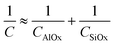
For characterizing the film electrically after calcination or ozonation, we used a metal oxide semiconductor (MOS) capacitance. On an n-type silicon wafer, we prepared a porous film of aluminium oxide onto which we deposited a patterned layer of gold. The resulting MOS structure (Fig. 4E) consisted of two dielectric layers embedded between a semiconductor substrate (i.e. silicon) and a metal electrode (i.e. gate). The top dielectric layer (AlOx in Fig. 4E) was the calcined or ozonized CCL-PAA/Al3+ film we prepared; the lower dielectric was a layer of silicon oxide (SiOx in Fig. 4E) grown naturally on the silicon substrate during calcination/ozonation of the sample in an air atmosphere. The total capacitance (C) of the MOS structure can be obtained by combining the capacitances of each of the dielectric layers (CAlOx and CSiOx) and that of the silicon substrate (CSi) in series:
 | (2) |
We considered the capacitances associated with the dielectric layers (CAlOx and CSiOx) to be constant because the applied voltages were far from the breakdown voltage of these layers. The capacitance of silicon (CSi) depends dramatically on gate voltage (vG), since it determines the charge of the interfacial region of silicon, i.e. the region of the silicon substrate adjacent to the layer of silicon oxide.
In the most general case, the gate voltage has both DC (gate bias, VG) and AC  components:
  . For our measurements, we applied a gate bias (VG) ramping from −3 V to 3 V and back to −3 V at 0.1 V sec−1, and an AC voltage (
 , amplitude of 0.1 V and frequency of 4 MHz), superposed to the DC ramp, as illustrated in Fig. 4G. Each component of the applied gate voltage determines a different type of capacitance. The gate bias sets the quasi-static polarization point of the MOS structure that establishes its static capacitance (Cstat = QT/VG, where QT stands for the total charge of the interfacial layer);
  sets the high frequency conditions for evaluating the differential capacitance (C = dQT/dVG) of the MOS structure. The static and differential capacitances can be very different due to the nonlinear response of an MOS structure to gate voltage.40 Of the two, the differential capacitance is the parameter of interest in applications of signal processing (high operation frequency and small amplitude) because it provides the rate of change of charge with voltage.
Fig. 4H shows a typical curve of the differential capacitance measured for MOS structures containing either a calcined or an ozonized aluminium oxide film. When a positive gate bias (VG > 0) was applied, positive charges collected at the interface between the metal gate and the top dielectric (aluminium oxide, in our case) and attracted negative charges from the silicon substrate to the interface between silicon and the bottom dielectric layer (here, silicon oxide); the dielectric layers prevent the actual flow of charges between gate and silicon. Therefore, after applying VG > 0, electrons (i.e. the majority carriers in n-type silicon) accumulated at the silicon interface layer, which yielded the MOS capacitance under accumulation. At high positive voltages, the density of electrons at the interface was so high that the capacitance associated with the interface became much greater than that of the dielectric layers such that eqn (2) could be simplified to eqn (3):
 | (3) |
As discussed, capacitance of dielectric layers does not depend on the applied gate voltage; at VG > 0, C tended to stabilize to its highest value and the curve in Fig. 4H reached a plateau. As the gate bias decreased, electrons were less attracted to the silicon interface; the charge at the interface decreased, as did the interface capacitance. As CSi became comparable to the capacitance of the dielectric layers, the curve of capacitance started to decrease, leaving the plateau. A negative gate voltage (VG < 0) would accumulate negative charges in the metal gate and repel electrons, thus depleting the interface silicon layer of majority carriers. This situation is known as the depletion state of the MOS capacitor.
By applying a negative voltage of larger magnitude (VG
≪ 0) than that required for repelling the electrons, minority carriers (holes) were attracted to the silicon interface in order to balance the increased negative charge collected at the gate. Thus, large negative voltages created, at the silicon interface, a layer of net charge with sign opposite (positive) to that of the majority carriers (negative), which yielded the MOS capacitance to its inversion state. The bias voltage (VG, DC gate voltage) drove minority carriers to accumulate at the interface, and increased the static capacitance (Cstat) of the silicon interface. The differential capacitance (C), though, is determined by the ability of charges to follow the oscillations of the AC gate voltage  , i.e. by the charge carrier response time, which depends inversely on the local volumetric density of charge carriers. The response time of majority carriers will be much higher than that of minority carriers for a given |VG|. At the frequency we used in our measurements (4 MHz), majority carriers could follow the AC gate voltage
  , but minority carriers could not respond as rapidly as required by
  . The curves shown in Fig. 4H agree with the previous statement: while at positive bias voltages the accumulation of majority carriers at the silicon interface led to a large value of CSi, at negative VG the accumulation of minority carriers resulted in a CSi smaller than that of the dielectric layers. As a consequence, the differential capacitance of the MOS structure reaches its minimum value in inversion, dominated by the capacitance of the silicon interface (eqn (4)):
| C ≈ CSi | (4) |
In order to determine the dielectric constant (k) of the aluminium oxide layer, we used the value of C at VG = 3 V (Fig. 4H), where eqn (3) is valid and C depends only on the capacitance of the dielectric layers. We can model each of the dielectric layers as a planar capacitor, where d stands for the thickness of the dielectric layer, A for the area of the electrode (5.6 × 10⁻⁸ m2), and ε0 for the permittivity of free space (8.85 × 10⁻¹² F m−1) (eqn (5)):
 | (5) |
We determined the thickness of the silica interfacial layers by ellipsometry: d = 10.5 nm for the calcined film and d = 3.2 nm for the ozonized film. First, we obtained CSiOx after substituting kSiO2, ε0, dSiOx, and A in eqn (5).41 Second, we calculated CAlOx from eqn (3) and the values of CSiOx and C at 3 V. Last, we determined the dielectric constant of the aluminium oxide film (kAlOx) from eqn (5): kAlOx ≈ 3.5 for the calcined films, and ≈3.2 for the ozonized films. The dielectric constants we obtained for the aluminium oxide substrates are not considered to be very low (currently 1.5–2.5), but they do represent a > 60% reduction of the dielectric constant from its bulk value (9.34).42 This technique also expands the methods for making low-k dielectrics and the types of inorganic materials that can be used for low-k dielectric substrates.
Fig. 4H shows that the maximum value of capacitance reached by the calcined sample is about twice that reached by the ozonized sample. Since the dielectric constants calculated for both samples are similar (3.5 and 3.2), and according to eqn (5), the difference in the maximum values reached by each sample reflects the fact that the thickness of the aluminium layers in the calcined film is about half the thickness of the ozonized film—as detailed above, ∼23 nm and ∼49 nm, respectively. Also, the calcined film showed less hysteresis than the ozonized film. Hysteresis in measurements of MOS capacitance measurements is the consequence of the presence of dopant impurities trapped in the dielectric layer. These species, after becoming polarized by an initial gate voltage, require a larger gate voltage opposing the initial one in order to reorient. Hysteresis is undesirable for many electronic applications of low-k dielectric films, as it forces a wider operating voltage range to reverse the stored charge across a capacitor.
Current leakage in dielectric materials is quantified by dispersion, which is defined as the ratio of the real to the imaginary component of the complex impedance; an ideal capacitor with no leakage would have a dispersion of zero. We measured lower dispersion values for the calcined film (∼0.6) than for the ozonized film (∼2.8); both values were less than the typically accepted upper limit for current leakage (typically <3). Some of the increased leakage for the ozonized film can be attributed to a thinner underlying SiO2 layer (3.2 nm) than in the calcined samples (10.5 nm).
Conclusions
Using photolithography, we patterned PAA films cross-linked with metal cations. The patterned cross-linked film acts as an ion-exchange resin that allows one cation to be exchanged for another. Also, reduction of these metal cations generates nanoparticles within a patterned polymer matrix. Calcination or ozonation of a metal-containing film creates porous thin films of metal oxide that function as low-k dielectric materials.In comparison to other methods for patterning thin polymer films, the advantages of using this technique to pattern a CCL-PAA film include the ability i) to use standard photolithographic processes to yield CCL-PAA structures as small as 500 nm, ii) to pattern a wide array of both continuous and discontinuous patterns in CCL-PAA, iii) to incorporate a wide range of cross-linking agents, and iv) to exchange the cations reversibly in the matrix without degradation of the pattern. Of course, this technique inherits all of the disadvantages of standard photolithography—e.g. the limitations on resolution and the necessity of clean-room facilities. There is not a single universal procedure for creating CCL-PAA films: empirical optimization of the etching conditions for each cation is required.
A metal-containing ion-exchange resin patterned with high edge resolution could generate patterned catalytic surfaces, tailor surface chemistry for “lab-on-a-chip” devices, or yield fluorescent or optically-active surfaces containing semiconducting or metallic nanostructures. The use of standard photolithographic processes and materials enables this technology to be incorporated easily into current fabrication processing, and expands the types of materials available for microelectronics.
Experimental
All materials were purchased and used as received unless otherwise stated.Formation of the CCL-PAA film
We exposed either a silicon wafer or a glass slide to an oxidizing (air) plasma in a plasma cleaner (∼266 Pa, 100 W, Harrick Scientific Model PDC-32G) for 1 minute. A solution of PAA (Mw ≈ 100![[thin space (1/6-em)]](https://www.rsc.org/images/entities/char_2009.gif) 000; Aldrich) adjusted with KOH (Fluka) to 3.5% w/v and a pH ≈ 2.5 was spun-cast (1500 rpm for 15 seconds) and baked for 15 minutes at 150 °C on a hot plate. A second layer of PAA (3.5% w/v, pH ≈ 7.2) was spun (1500 rpm for 15 seconds) onto the substrate and baked for 2 minutes at 150 °C. We immersed the substrate in an aqueous solution (typically 1 M) containing the cross-linking metal salt for 1 minute, rinsed the film with water and dried it under a stream of N2.
000; Aldrich) adjusted with KOH (Fluka) to 3.5% w/v and a pH ≈ 2.5 was spun-cast (1500 rpm for 15 seconds) and baked for 15 minutes at 150 °C on a hot plate. A second layer of PAA (3.5% w/v, pH ≈ 7.2) was spun (1500 rpm for 15 seconds) onto the substrate and baked for 2 minutes at 150 °C. We immersed the substrate in an aqueous solution (typically 1 M) containing the cross-linking metal salt for 1 minute, rinsed the film with water and dried it under a stream of N2.
Patterning
Onto the CCL-PAA film, we spun-cast a film of positive photoresist (either S1813 or S1805 (Rohm and Haas) depending on the size of our features) at 500 rpm for 5 seconds and 3000 rpm for 30 seconds. After baking the photoresist for 3 minutes at 110 °C, we exposed it for 3 seconds to UV radiation with an AB-M mask-aligner. The substrates were developed in a 0.7 M NaOH solution (Microposit 351 developer (Rohm and Haas) diluted 1 : 1 with water) for 4–10 seconds, or a 0.26 M TMAH solution (MF-26A developer (Rohm and Haas)) for 30–45 seconds, depending on the cross-linking metal. The substrates were rinsed with deionized water and dried under N2. Afterwards, if necessary, the substrates were immersed in an aqueous 0.5 M EDTA solution (pH 8.2, Sigma) in order to etch the CCL-PAA film. Finally, we rinsed the substrates with acetone to remove the undeveloped photoresist and to yield a patterned CCL-PAA film. All optical images were obtained on a Leica DMRX microscope; AFM micrographs were collected in tapping mode with a Digital Instruments Dimension 3100 Nanoscope, and analyzed using the Nanoscope IV v5.12b18 software.Fluorescent imaging
For imaging the films with a fluorescent molecule embedded in the CCL-PAA matrix, a mercury lamp with an arclamp power supply (LEP Ltd.) was used. The images were recorded by a Hamamatsu ORCA-ER camera with exposure times of 200 milliseconds for the rhodamine B film. For imaging the CCL-PAA/DAH films, a CCD camera (Nikon DXM1200) was used with excitation and emission filters of λex = 470–490 nm and λem > 515 nm respectively and exposure times of 20 milliseconds.Cation reduction
The CCL-PAA/Ag+ film was reduced under a UV lamp (long-wave mercury lamp, 100 W) for 20 minutes. An aqueous solution (10 mL) containing 0.1 M borane dimethylamine complex (CAS 74-94-2, Strem Chemicals) and 1 M CaCl2 reduced the CCL-PAA/Pd2+ film in 1 minute.Low-k dielectrics
Before spin-casting the PAA films, the silicon wafers were etched for 1 minute in HF (∼5%) followed by a UV/ozone treatment for 3 minutes. The CCL-PAA/Al3+ films were calcined in a furnace (Thermolyne) at 750 °C for 4 hours. The CCL-PAA/Al3+ films were ozonized for 3 hours. Gold electrodes (with an area of 5.6 × 10⁻⁸ m2, and a thickness of ∼25 nm) were evaporated onto the sample through a hard mask using a sputter coater (Cressington 208HR). A gold contact (∼25 nm) was evaporated onto the back of the silicon substrate to ensure ohmic contact between the Si and the probe during measurements. We measured the capacitance on a probe station (Sigmatone) with a LCR meter (HP 4275A). The thickness of the SiO2 layer was measured by ellipsometry (Rudolph Research AutoEL) at 632.8 nm.Acknowledgements
This research was supported by the NIH award (NIH GM065364) and used the shared Resource Facilities supported by the National Science Foundation under NSEC (PHY-0117795) and MRSEC (DMR-0213805) awards. R. P.-C. gratefully acknowledges the Generalitat de Catalunya (DURSI) for support in the form of a postdoctoral fellowship. M. N. acknowledges funding from an NIH fellowship (T32-GM07598). The authors would like to thank Dr E. Weiss and Mr L. McCarty for useful conversations.References
- L. J. Guo, J. Phys. D: Appl. Phys., 2004, 37, R123 CrossRef CAS.
- S. R. Forrest, Nature, 2004, 428, 911 CrossRef CAS.
- Y. N. Xia and G. M. Whitesides, Annu. Rev. Mater. Sci., 1998, 28, 153 CrossRef CAS.
- H. Ma, A. K. Y. Jen and L. R. Dalton, Adv. Mater., 2002, 14, 1339 CrossRef CAS.
- T. Velten, H. H. Ruf, D. Barrow, N. Aspragathos, P. Lazarou, E. Jung, C. K. Malek, M. Richter and J. Kruckow, IEEE Trans. Adv. Packag., 2005, 28, 533 CrossRef.
- S. I. Stupp, J. Donners, L. S. Li and A. Mata, MRS Bull., 2005, 30, 864 CAS.
- X. Jiang and G. M. Whitesides, Eng. Life Sci., 2003, 3, 475 CrossRef CAS.
- K. E. Gonsalves, L. Merhari, H. P. Wu and Y. Q. Hu, Adv. Mater., 2001, 13, 703 CrossRef CAS.
- D. G. Lidzey, M. Voigt, C. Giebeler, A. Buckley, J. Wright, K. Bohlen, J. Fieret and R. Allott, Org. Electron., 2005, 6, 221 Search PubMed.
- D. B. Wolfe, J. B. Ashcom, J. C. Hwang, C. B. Schaffer, E. Mazur and G. M. Whitesides, Adv. Mater., 2003, 15, 62 CrossRef CAS.
- W. R. Childs and R. G. Nuzzo, J. Am. Chem. Soc., 2002, 124, 13583 CrossRef CAS.
- E. Kim, Y. N. Xia and G. M. Whitesides, Nature, 1995, 376, 581 CrossRef CAS.
- J. A. Rogers, Z. N. Bao and V. R. Raju, Appl. Phys. Lett., 1998, 72, 2716 CrossRef CAS.
- Y. V. X. Lit, W. Hit, Y. Ma, L. B. Zhang, J. Q. Sun, N. Lu and L. C. Shen, Macromol. Rapid Commun., 2006, 27, 505 CrossRef.
- K. Y. Suh, Y. S. Kim and H. H. Lee, Adv. Mater., 2001, 13, 1386 CrossRef CAS.
- G. Tae, R. G. H. Lammertink, J. A. Kornfield and J. A. Hubbell, Adv. Mater., 2003, 15, 66 CrossRef CAS.
- Y. S. Kim, J. Park and H. H. Lee, Appl. Phys. Lett., 2002, 81, 1011 CrossRef CAS.
- I. S. Lee, P. T. Hammond and M. F. Rubner, Chem. Mater., 2003, 15, 4583 CrossRef.
- H. Tokuhisa and P. T. Hammond, Adv. Funct. Mater., 2003, 13, 831 CrossRef CAS.
- B. D. Gates, Q. B. Xu, J. C. Love, D. B. Wolfe and G. M. Whitesides, Annu. Rev. Mater. Res., 2004, 34, 339 CrossRef CAS.
- B. D. Gates, Q. B. Xu, M. Stewart, D. Ryan, C. G. Willson and G. M. Whitesides, Chem. Rev., 2005, 105, 1171 CrossRef CAS.
- M. Husemann, M. Morrison, D. Benoit, K. J. Frommer, C. M. Mate, W. D. Hinsberg, J. L. Hedrick and C. J. Hawker, J. Am. Chem. Soc., 2000, 122, 1844 CrossRef CAS.
- S. J. Martin, J. P. Godschalx, M. E. Mills, E. O. Shaffer and P. H. Townsend, Adv. Mater., 2000, 12, 1769 CrossRef CAS.
- K. Maex, M. R. Baklanov, D. Shamiryan, F. Iacopi, S. H. Brongersma and Z. S. Yanovitskaya, J. Appl. Phys., 2003, 93, 8793 CrossRef CAS.
- S. J. Ding, P. F. Wang, D. W. Zhang, J. T. Wang and W. W. Lee, Mater. Lett., 2001, 49, 154 CrossRef CAS.
- R. Schwodiauer, G. S. Neugschwandtner, S. Bauer-Gogonea, S. Bauer and T. Rosenmayer, Appl. Phys. Lett., 2000, 76, 2612 CrossRef CAS.
- R. Roy, Science, 1987, 238, 1664 CrossRef CAS.
- Y. K. Akimov, Instrum. Exp. Tech., 2003, 46, 287 CrossRef CAS.
- L. Esposito, G. Ottaviani, E. Carollo and M. Bacchetta, Appl. Phys. Lett., 2005, 87.
- J. H. Yim, M. R. Baklanov, D. W. Gidley, H. G. Peng, H. D. Jeong and L. S. Pu, J. Phys. Chem. B, 2004, 108, 8953 CrossRef CAS.
- J. L. Hedrick, T. Magbitang, E. F. Connor, T. Glauser, W. Volksen, C. J. Hawker, V. Y. Lee and R. D. Miller, Chem.–Eur. J., 2002, 8, 3308 CrossRef CAS.
- C. J. Hawker, J. L. Hedrick, R. D. Miller and W. Volksen, MRS Bull., 2000, 25, 54 CAS.
- V. Linder, B. D. Gates, D. Ryan, B. A. Parviz and G. M. Whitesides, Small, 2005, 1, 730 CrossRef CAS.
- Critical Stability Constants, ed. A. E. Martell and R. M. Smith, Plenum, New York, 1974 Search PubMed.
- F. A. Cotton and G. Wilkinson, Advanced Inorganic Chemistry, John Wiley & Sons, New York, 1988 Search PubMed.
- V. Linder, H. K. Wu, X. Y. Jiang and G. M. Whitesides, Anal. Chem., 2003, 75, 2522 CrossRef CAS.
- One parameter that appeared to have no effect on the relative rates of etching or the quality of the resulting structures was the temperature of the etching bath. We tried both cooling the bath (to ∼2 °C) and heating the bath (to ∼28 °C) to improve the resolution of this technique, but the quality of the pattern did not change.
- H. H. Huang, X. P. Ni, G. L. Loy, C. H. Chew, K. L. Tan, F. C. Loh, J. F. Deng and G. Q. Xu, Langmuir, 1996, 12, 909 CrossRef CAS.
- S. Eustis, G. Krylova, A. Eremenko, N. Smirnova, A. W. Schill and M. El-Sayed, Photochem. Photobiol. Sci., 2005, 4, 154 RSC.
- E. H. Nicollian and J. R. Brews, MOS (Metal Oxide Semiconductor) Physics and Technology, John Wiley & Sons, New York, 1982 Search PubMed.
- The value of kSiO2 used was 4 and the value of A used was 5.6 × 10⁻⁸ m2, the area of the gold pad that we evaporated onto our film.
- CRC Handbook of Chemistry and Physics, ed. L. I. Berger, CRC Press LLC, Boca Raton, FL, 85th edn, 2000 Search PubMed.
Footnote |
| † Electronic supplementary information (ESI) available: Schematical representation of under-etched or over-etched CCL-PAA film, and optical, AFM, SEM and TEM images of CCL-PAA films. See DOI: 10.1039/b611630b |
| This journal is © The Royal Society of Chemistry 2007 |