
Enhanced biocompatibility in poly(3-hexylthiophene)-based organic thin-film transistors upon blending with poly(2-(2-acetoxyacetyl)ethyl methacrylate)†
Na Kyung Kim‡
a,
Jin Woo Bae‡b,
Hyeon-Ki Jangc,
Jong-Chan Leea,
Kigook Songb,
Byung-Soo Kimac,
In Jun Parkd,
Jong-Wook Had,
Soo-Bok Leed and
Eun-Ho Sohn*d
aDepartment of Chemical and Biological Engineering, Institute of Chemical Processes, Seoul National University, Shilim-9-Dong, Gwanak-Gu, Seoul 151-744, Republic of Korea
bDepartment of Advanced Materials Engineering for Information and Electronics, Kyung Hee University, Yongin, Gyeonggi-do 446-701, Republic of Korea
cInterdisciplinary Program for Bioengineering, Seoul National University, Shilim-9-Dong, Gwanak-Gu, Seoul 151-744, Republic of Korea
dInterface Chemistry and Materials Center, Korea Research Institute of Chemical Technology, Daejon 305-343, Republic of Korea
First published on 2nd February 2016
Abstract
Polymer blends with both biocompatibility and organic thin film transistor (OTFT) characteristics are developed by mixing a biocompatible polymer, poly(2-(2-acetoxyacetyl)ethyl methacrylate) (PHEMAAA) and a conducting polymer, poly(3-hexyl thiophene) (P3HT) at different weight ratios (i.e. P3HT/PHEMAAA = 75/25, 50/50, 25/75). Their OTFT performances were maintained at a similar level to those of pristine P3HT in spite of adding an insulator in the form of PHEMAAA. On the other hand, the biocompatibility of the P3HT/PHEMAAA blend films was found to be as good as that of PHEMAAA, indicating the successful contribution of the biocompatible polymer. In particular, these combined properties were optimized at a 25/75 weight ratio as described above. These results could be correlated with surface properties such as molecular orientation, morphology, and composition that change upon blending. Such P3HT/PHEMAAA blends are promising materials for applications in biomedical fields where materials come into contact with the human body.
1. Introduction
Organic thin-film transistors (OTFTs) have been investigated by many research groups because of their numerous potential applications, ranging from flexible backings in active matrix displays to item-level radiofrequency identification tags.1–3 Recently, continued research on OTFTs has demonstrated their potential as a sensor platform, utilizing their effective transduction mechanism that can transform even a small induced external stimulus into more amplified electric signals.4 With high sensitivity, OTFT based-sensors are considered to be a strong candidate for disposable miniaturized chips, important for biomedical diagnostics, and can be used in both drug screening and toxicity tests.5,6 This biomedical test system is highly dependent on the biocompatibility and non-toxicity of the active layer for cell cultivation and long-term reporting without an inflammatory response.7,8 Therefore, several attempts to improve the biocompatibility of conducting polymers have been performed by blending the polymers with biomolecules, doping them with bioactive molecules, hydrogelation, and oxygen plasma treatment.9–12Among these techniques, blending is one of the most effective methods and can easily combine the beneficial properties of each component into one blended material. This method generally dominates over other chemical modifications of conducting polymers, in that it does not require any tedious or time-consuming processes. Several drawbacks of conducting polymers, such as low biocompatibility, mechanical strength, air stability, and high costs, could be mitigated by adding insulating polymers with high performance.13–15 However, conducting polymers blended with insulating polymers often suffer from degradation in device performances due to dilution effects.16 The dilution effect, however, can be overcome by connecting the conductive polymeric domains in the insulating polymer matrix through vertical phase-separated structures or nanowire networks.17,18 By controlling the blend structure, blending methods could be even more widely applicable and further reduce semiconductor costs.
P3HT is one of the more commonly used conducting polymers for OTFT systems, because it has high mobility (10−4 to 10−2 cm2 V−1 s−1) and good solubility in common solvents.19 However, the use of P3HT in biomedical applications can be limited due to their poor cell adhesion properties.9 There have been only a few studies of the improvement of biocompatibility of P3HT by blending with biocompatible insulating polymers, but these blends still suffer a loss in the conducting properties of P3HT.20 In this work, we impart biocompatibility into a P3HT-based OTFT system by blending it with poly(2-(2-acetoxyacetyl)ethyl methacrylate) (PHEMAAA), without any loss of the OTFT properties of P3HT. Previously, PHEMAAA was successfully synthesized and its excellent biocompatibility has been demonstrated.21 We believe that this is the first report demonstrating a biocompatible polythiophene system with acceptable OTFT performance created using a blending method.
2. Experimental
2.1. Materials
Poly(2-hydroxyethyl methacrylate) (PHEMA) (Mw = 300![[thin space (1/6-em)]](https://www.rsc.org/images/entities/char_2009.gif) 000 g mol−1) was purchased from Scientific Polymer Products (Ontario, NY, USA). Regioregular P3HT was obtained from Sigma-Aldrich (Mw ≈ 50000). Hexamethyldisilazane (HMDS) (99%) and acetoxyacetyl chloride (97%) were purchased from Sigma-Aldrich. Chloroform (CHCl3, 99.5%) and monochlorobenzene (MCB, 99.5%) purchased from Sigma-Aldrich were used as received. Microscope cover slides (25 mm) were purchased from Marienfeld GmbH & Co. KG (Lauda-Königshofen, Germany). PHEMAAA, as shown in Fig. 1, was synthesized according to previously reported procedures.21 Briefly, PHEMA (500 mg) was dissolved in 3 mL of pyridine, then acetoxy acetyl chloride (1.2 equiv.) diluted with 3 mL of tetrahydrofuran (THF) was added dropwise to the solution. The reaction proceeded for 12 h at room temperature, and the product could be obtained after several precipitation using water and methanol.
000 g mol−1) was purchased from Scientific Polymer Products (Ontario, NY, USA). Regioregular P3HT was obtained from Sigma-Aldrich (Mw ≈ 50000). Hexamethyldisilazane (HMDS) (99%) and acetoxyacetyl chloride (97%) were purchased from Sigma-Aldrich. Chloroform (CHCl3, 99.5%) and monochlorobenzene (MCB, 99.5%) purchased from Sigma-Aldrich were used as received. Microscope cover slides (25 mm) were purchased from Marienfeld GmbH & Co. KG (Lauda-Königshofen, Germany). PHEMAAA, as shown in Fig. 1, was synthesized according to previously reported procedures.21 Briefly, PHEMA (500 mg) was dissolved in 3 mL of pyridine, then acetoxy acetyl chloride (1.2 equiv.) diluted with 3 mL of tetrahydrofuran (THF) was added dropwise to the solution. The reaction proceeded for 12 h at room temperature, and the product could be obtained after several precipitation using water and methanol.
 | ||
| Fig. 1 Chemical structures of P3HT and PHEMAAA. | ||
2.2. Preparation of polymer blend films
1 wt% of P3HT, PHEMAAA, and their mixtures of P3HT and PHEMAAA with different mole ratios of 75/25, 50/50, and 25/75 were dissolved in a 1:1 (v/v) solvent mixture of CHCl3 and MCB. Both P3HT and PHEMAAA are well-dissolved in CHCl3, however, the mixture of CHCl3 and MCB was used as a solvent, because the poor solubility of P3HT in MCB could result in well-aligned P3HT crystal orientation, which can lead to favorable OTFT performance.22 The polymer solutions were sonicated at 40 °C until the solutions become transparent.
Silicon wafers were cleaned in a piranha solution (a mixture of concentrated sulfuric acid and hydrogen peroxide in a 7:3 ratio by volume) for 2 h followed by rinsing with ethanol (EtOH) and drying under nitrogen flow. The cleaned silicon wafers were treated with HMDS at 100 °C for 1 h to make their surfaces hydrophobic. The polymer solutions, filtered through a 0.45 μm PTFE syringe filter, were then spin-coated onto the HMDS-modified silicon wafers for morphology analysis, using a Laurell model WS-400A-6NPP/LITE spin coater at a rate of 3000 rpm for 30 s. The polymer films, having P3HT and PHEMAAA in the ratios of 75/25, 50/50, and 25/75, are named as 75/25 blend, 50/50 blend, and 25/75 blend, respectively. For cell tests, all samples were prepared as described above but on the glass substrates.
2.3. Surface characterization
Grazing incidence wide-angle X-ray diffraction (GIWAXD) was performed using a high-power X-ray beam (photon flux ≈ 1011 photons s−1 mrad−1 per 0.1%, beam size ≤ 0.5 mm2) from a synchrotron radiation source (3C beamline, Pohang Accelerator Laboratory, Korea) at λ = 1.1352 Å. The detection system was equipped with a 2D X-ray detector (PI-SCX4300-165/2, Princeton Instruments). The scattering angles were corrected according to the positions of the X-ray beams reflected from the silicon substrate interface with changing incidence angle (αi), and with respect to pre-calibrated silver behenate (AgC22H43O2).The surface topologies of the polymer films were obtained using tapping-mode atomic force microscopy (AFM; SPA 400 with a SPI 3800 controller, Seiko Instruments Industry, Co. Ltd., Japan) using a silicon nitride cantilever (NCH Point Probe, Nano world, Neuchtel, Switzerland) with a resonance frequency of 320 kHz and a spring constant of 42 N m−1. The root-mean-square (RMS) roughness values were taken from the topography images of a 5 × 5 μm2 area at room temperature.
X-ray photoelectron spectroscopy (XPS) experiments were performed in an UHV multipurpose surface analysis system (Thermo Scientific, Sigma Probe, UK) operating at base pressures <10−10 mbar. For acquisition of photoelectron spectra, the constant analyzer energy (CAE) mode was employed at a pass energy of 40 eV and a step of 0.1 eV at a takeoff angle of 90°.
2.4. OTFT characteristics
Bottom-gate, top-contact devices were fabricated on highly doped p-type Si with a 300 nm SiO2 dielectric layer. Silicon wafers were cleaned by sonication of the substrates in acetone and isopropyl alcohol (IPA), followed by drying with nitrogen. The silicon wafers were then treated with atmospheric oxygen plasma for 5 min at a fixed RF power of 100 W at a frequency of 13.56 MHz (Emitech K1050X). Argon (5 Lpm) and oxygen (20 sccm) were used as the carrier and reactive gases, respectively. After plasma treatment, Si/SiO2 was hydrophobically treated with hexamethyldisilazane (HMDS) to prevent charge trapping by R–OH functional groups. The P3HT and P3HT/PHEMAAA blend solutions with different weight ratios of 75/25, 50/50, and 25/75 were dissolved at a concentration of 1 wt% in MCB/CHCl3 (1:1 v/v). Filtered through a 0.45 μm PTFE syringe filter, the solutions were then spun-cast onto the HMDS-modified silicon wafers at a rate of 3000 rpm for 30 s, using a Laurell model WS-400A-6NPP/LITE spin coater, then annealed at 200 °C for 30 min. All procedures and measurements were carried out in a glove box under dry argon gas. In order to make electrical contact, source drain electrodes were patterned by placing thin steel shadow masks on top of the substrate, and thermally evaporating a 50 nm gold layer on top. The pressure in the chamber was maintained at about 10−6 mbar and the voltage applied across the heating coil controlled to keep evaporation rates of 0.1 Å s−1. The devices were fabricated with variable channel lengths (L) of 20–100 μm and widths (W) of 0.5–2 mm, respectively.
The electrical characteristics of the OTFT devices were measured at room temperature under ambient conditions using an Agilent 4155C semiconductor parameter analyzer. Typically, several output curves were recorded for different gate voltages, and transfer curves were measured in both the linear and saturation regimes of the OTFT. Numerical differentiation of IDS with respect to VGS allows the field-effect transistor mobility (μ) to be calculated in the saturation regimes using eqn (1), where W, L, Ci, and Vt are the channel width, channel length, the capacitance per unit area of the dielectric layer, and the threshold voltage, respectively. The field-effect mobility values in the saturation region were calculated from the slope of the square root of the drain-source current as a function of the gate-source voltage, i.e. |IDsat|1/2 versus Vg plot (eqn (1)). Average data were calculated from analysis of 10 independent devices.
 | (1) |
2.5. Cytotoxicity tests
Human dermal fibroblasts (HDFs) were cultured in Dulbecco's modified Eagle's medium (DMEM, Gibco BRL, Gaithersburg, MD, USA) supplemented with 10% (v/v) fetal bovine serum (FBS, Gibco BRL) and 100 units per mL penicillin (Gibco BRL) and 100 mg mL−1 streptomycin (Gibco BRL). To test the biocompatibility of P3HT, PHEMAAA, and their blend films, cells were seeded on polymer films at a density of 5 × 10³ cells per cm2 and maintained in DMEM (Gibco BRL) supplemented with 10% (v/v) FBS (Gibco BRL), 100 units per mL penicillin (Gibco BRL), and 100 mg mL−1 streptomycin (Gibco BRL).The viability of the HDFs was evaluated using a colorimetric test based on the uptake of neutral red (3-amino-7-dimethylamino-2-methylphenazine hydrochloride) dye into viable cells. In brief, HDFs were rinsed with phosphate-buffered saline (PBS, Sigma Aldrich, St. Louis, MO, USA) and incubated for 3 h at 37 °C in DMEM containing neutral red (50 μg mL−1, Sigma). After removing the medium, a solution of 1% (v/v) acetic acid and 50% (v/v) ethanol was added to extract the dye. After 5 min of incubation at room temperature, the absorbance was read at 540 nm. The viability of the HDFs was expressed as a percentage of the absorbance of a PHEMAAA-positive control. On day 4, the morphology of HDFs was evaluated using light microscopy (IX71, Olympus, Tokyo, Japan).
Live and dead cells were detected with fluorescence microscopy (DS-2U, Nikon, Japan) after staining with fluorescein diacetate (FDA, Sigma Aldrich) and ethidium bromide (EB, Sigma-Aldrich) 4 d after seeding. The cells cultured on the blend films were incubated in FDA/EB (5 μg mL−1, 10 μg mL−1, respectively) for 5 min at 37 °C and then washed twice in PBS (Sigma-Aldrich). Dead cells were stained red due to the nuclear permeability of EB. Viable cells, capable of converting the non-fluorescent FDA into fluorescein, were stained green. The surface images were obtained by using a confocal laser scanning microscopy (CLSM, Eclipse 90i, Nikon, Japan).
3. Results and discussion
3.1. OTFT properties
P3HT and the blend films with different weight ratios of P3HT/PHEMAAA = 75/25, 50/50, and 25/75 were used as an active layer of OTFT devices for determining their electrical properties. Output and transfer curves of OTFTs with the blend films are shown in Fig. S1† and the OTFT characteristics, such as the field-effect mobility (μ), current on/off ratio (Ion/Ioff), and threshold voltage (Vt) obtained from the transfer curve are briefly summarized in Table 1. The hole mobility value based on the P3HT film was observed to be 7.6 × 10⁻³ cm2 V−1 s−1, which is close to the other reported values prepared from P3HT.17 The hole mobility values of OTFT devices prepared using the P3HT/PHEMAAA blend films were found to be only slightly smaller than that from P3HT film, despite the presence of the PHEMAAA insulator. In particular, the value was maintained on the order of 10−3 even when the blend included 75 wt% PHEMAAA (25/75 blend). Since the hole mobility values were calculated using only the dielectric constant of the SiO2 layer, without consideration of the much lower dielectric constant of PHEMAAA, for all blends they are expected to be higher in experimental conditions than in theory. In addition, OTFT devices based on P3HT/PHEMAAA blend films showed on–off current ratios that are greater by two orders of magnitude for all samples, and their threshold voltages (Vt) were in the range of −2.9 to −6.1 V, comparable to those of OTFT devices from P3HT blend systems reported previously.18 This result can be attributed to the formation of effective conductive networks of P3HT molecules, which can help to generate charge transportation.23 Also, this indicates the minimal influence of PHEMAAA on the OTFT properties caused by phase separation between each polymer component. This could be correlated with other surface properties such as molecular orientation, morphology, and composition as discussed below.| d-Spacing | P3HT | P3HT/PHEMAAA (wt%) | ||
|---|---|---|---|---|
| 75/25 | 50/50 | 25/75 | ||
| Mobility, μ (cm2 V−1 s−1) | 7.6 × 10⁻³ | 4.4 × 10⁻³ | 3.9 × 10⁻³ | 3.2 × 10⁻³ |
| Ion/Ioff | 8.2 × 10² | 9.0 × 10² | 1.4 × 10² | 3.4 × 10² |
| Vt | −2.9 | −2.6 | −6.1 | −3.9 |
3.2. Surface properties
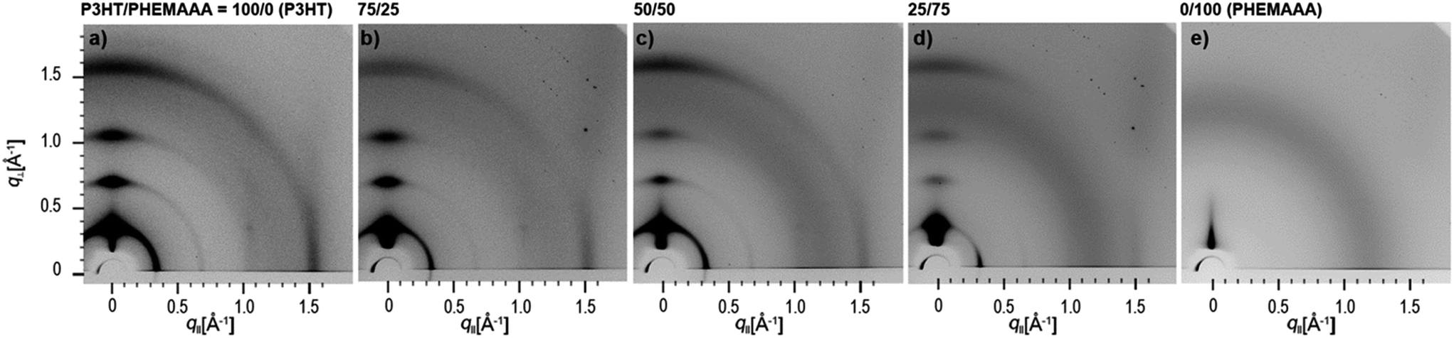 | ||
| Fig. 2 GIWAXD 2D patterns of (a) P3HT, (b) 75/25 blend, (c) 50/50 blend, (d) 25/75 blend, and (e) PHEMAAA films. | ||
 | ||
| Fig. 3 AFM height images (5 μm × 5 μm) of (a) P3HT, (b) 75/25 blend, (c) 50/50 blend, (d) 25/75 blend, and (e) PHEMAAA films, and (f–j) corresponding line profiles. | ||
The phase-separated structures of the polymer blends can be better understood by observing the surface structures obtained after selective dissolution of the P3HT fraction in the blends using MCB. Fig. 4 shows that the island structures of the 75/25 and 50/50 blend surfaces become clearer by removal of the P3HT. Accordingly, the roughness value of the 75/25 blend surface increased from 3.3 nm to 9.1 nm and that of the 50/50 blend also increased from 12.9 nm to 15.1 nm. On the other hand, the 25/75 blend with less P3HT did not show any differences before and after the solvent treatment. These results can be explained by a proposed model, which predicts the configuration of the blend domains according to the blend composition as displayed in Fig. 5. When the P3HT content is relatively high (i.e. in the 75/25 and 50/50 blends), a large amount of P3HT domains might be located at the surface along with PHEMAAA domains. Therefore, the removal of the P3HT domains on the blend surfaces results in a larger roughness value by increasing the height of islands. However, the roughness value of the 25/75 blend remained almost constant, even after selective dissolution of the P3HT, as these domains were mainly located on the lower regions of the film, which are difficult for the etching solvent to access. Due to the phase-separated structure of the blends, P3HT can establish conductive networks with well-ordered lamellar structures in the larger PHEMAAA matrix. The connective networks of P3HT domain were clearly observed from inner parts of all the blend films by investigating SEM images obtained after selective dissolution of PHEMAAA domains (Fig. S2†).
 | ||
| Fig. 4 AFM topographic 3D images of the 75/25 blend, 50/50 blend, and 25/75 blend surfaces (a) before and (b) after selective dissolution of P3HT part with MCB. | ||
 | ||
| Fig. 5 A schematic diagram explaining the change of surface morphology before and after selective dissolution of P3HT according to blend composition: (a) 75/25 blend, (b) 50/50 blend, and (c) 25/75 blend. | ||
![[double bond, length as m-dash]](https://www.rsc.org/images/entities/char_e001.gif) O moiety at 532.5 eV, and a peak from the C–O moiety at 533.9 eV. In addition, the S2p of the C–S moiety was measured at 163.1 and 164.3 eV. Fig. 6b shows the O/S ratios of the P3HT/PHEMAAA blend films before and after dissolution in MCB. Before the selective removal of P3HT domains, the O/S ratios of the 75/25 and 50/50 blend surfaces are similar and smaller than those of 25/75 blend. This result suggests that the 75/25 and 50/50 blend surfaces are mainly occupied by the thiophene groups of P3HT, while in the case of 25/75 blend, a greater amount of PHEMAAA exists in the upper region of the film. After dissolution of the P3HT domains, the O/S ratios of all polymer surfaces increase due to the increased proportion of PHEMAAA content. On the other hand, the relatively low value of the O/S ratio in the 25/75 blend surface arises from the large amount of PHEMAAA covering the P3HT domain on the surface before the solvent etching. These results could be well-correlated with the observations made in Section 3.2.2. These compositional differences might be based on the clear phase separation between P3HT and PHEMAAA with the formation of the different domain size of each polymer part according to the blend composition. On the other hand, the influence of surface energy on the phase-separated structure of the blend films is considered to be marginal because the surface energy of P3HT (34.3 mN m−1) is quite lower than that of PHEMAAA (44.6 mN m−1) as shown in Table S2;† it has been reported that a polymer part with lower surface energy tends to migrate toward the top surface.27,28 On the other hand, quite a few researchers suggested that the phase-separated structure of blends could be determined by various factors, such as solvent choice and polymer–substrate interaction besides surface energy of polymers.29,30
O moiety at 532.5 eV, and a peak from the C–O moiety at 533.9 eV. In addition, the S2p of the C–S moiety was measured at 163.1 and 164.3 eV. Fig. 6b shows the O/S ratios of the P3HT/PHEMAAA blend films before and after dissolution in MCB. Before the selective removal of P3HT domains, the O/S ratios of the 75/25 and 50/50 blend surfaces are similar and smaller than those of 25/75 blend. This result suggests that the 75/25 and 50/50 blend surfaces are mainly occupied by the thiophene groups of P3HT, while in the case of 25/75 blend, a greater amount of PHEMAAA exists in the upper region of the film. After dissolution of the P3HT domains, the O/S ratios of all polymer surfaces increase due to the increased proportion of PHEMAAA content. On the other hand, the relatively low value of the O/S ratio in the 25/75 blend surface arises from the large amount of PHEMAAA covering the P3HT domain on the surface before the solvent etching. These results could be well-correlated with the observations made in Section 3.2.2. These compositional differences might be based on the clear phase separation between P3HT and PHEMAAA with the formation of the different domain size of each polymer part according to the blend composition. On the other hand, the influence of surface energy on the phase-separated structure of the blend films is considered to be marginal because the surface energy of P3HT (34.3 mN m−1) is quite lower than that of PHEMAAA (44.6 mN m−1) as shown in Table S2;† it has been reported that a polymer part with lower surface energy tends to migrate toward the top surface.27,28 On the other hand, quite a few researchers suggested that the phase-separated structure of blends could be determined by various factors, such as solvent choice and polymer–substrate interaction besides surface energy of polymers.29,30
 | ||
| Fig. 6 The representative XPS S2p and O1s core level spectra on the surfaces of (a) 25/75 blend and (b) O/S ratios of P3HT/PHEMAAA blend films before (black square line) and after MCB treatment (red triangle line). | ||
3.3. Cell viability
To investigate the biocompatibility of the P3HT/PHEMAAA blend films, both quantitative and qualitative tests were carried out using HDFs. First, neutral red assays were performed for 4 d to determine the viability of cells cultured on P3HT, PHEMAAA, and the P3HT/PHEMAAA blend films. Since only live cells cultured on the samples can absorb the neutral red dye, cell viability results could be quantitatively obtained by measurement of the optical density. Fig. 7 shows the viability of HDFs, which were cultured on P3HT, PHEMAAA, and the P3HT/PHEMAAA blend films. Here, PHEMAAA was chosen as a positive control because the excellent biocompatibility of PHEMAAA has been fully demonstrated in the past.21 Moreover, the poor viability of cells cultured on P3HT could be observed with optical microscopy (Fig. 7a). It has been previously reported that unmodified P3HT surfaces show poor cell adhesion.9 Fig. 7f shows that only 25 wt% of PHEMAAA is needed to drastically enhance the viability of cells cultured on P3HT. Moreover, the significantly larger surface coverage of HDFs on the P3HT/PHEMAAA blend films supported the enhancement of cell viability owing to the presence of PHEMAAA domains (Fig. 7e). In particular, the 25/75 blend film has the highest content of PHEMAAA among the blend ratios and exhibits almost same cell viability as that of PHEMAAA. | ||
| Fig. 7 Representative optical microscopy images of HDFs cultured for 4 days on (a) P3HT, (b) 75/25 blend, (c) 50/50 blend, (d) 25/75 blend, (e) PHEMAAA films, and (f) the quantitative results (scale bar = 100 μm). | ||
The cytotoxicity of the P3HT/PHEMAAA blend films was also evaluated using a qualitative assay of live/dead cells, wherein live cells are stained green and the nuclei of dead cells are stained red. Fig. 8 shows that most of the cells are alive with no apparent red signals from any of the blend films. This result indicates that none of the P3HT/PHEMAAA blend films shows any cytotoxic behavior on their surfaces, demonstrating their huge potential to be applied as implantable electronic devices. Furthermore, the effects of PHEMAAA content on the biocompatibility of the blend films are consistent with the results discussed for the neutral red assay; the CLSM images also show that increased PHEMAAA content in the blend solutions could improve the cell viability of the blend films. In particular, the surface of the 25/75 blend film is the most abundant in green-stained HDFs, comparable to that observed on PHEMAAA.
 | ||
| Fig. 8 CLSM images presenting FDA/EB staining on HDFs cultured for 4 d on (a) P3HT, (b) 75/25 blend, (c) 50/50 blend, (d) 25/75 blend, and (e) PHEMAAA films (scale bar = 100 μm). | ||
Considering the results of both cell tests, the viability of cells cultured on the P3HT/PHEMAAA blend films was found to increase with the addition of PHEMAAA. Since the surface (which comes in direct contact with the cell) is composed mostly of PHEMAAA, the cells could be more active than when they were cultured on the surface of P3HT. In particular, the 25/75 blend has the highest PHEMAAA content among all the blend films and shows biocompatibility comparable to that of PHEMAAA. Additionally, the greater surface roughness could play a role in accelerating cell adhesion and proliferation, based on previous reports.21
4. Conclusion
In conclusion, we successfully developed biocompatible semiconducting films by blending of a polymer semiconductor (P3HT) and a biocompatible polymer (PHEMAAA). All of the P3HT/PHEMAAA blend films having more than 25 wt% of P3HT showed stable OTFT performances comparable to those of P3HT, which indicates that efficient connective conductive networks could be formed in the blend films without a critical disturbance of PHEMAAA. The biocompatibility of P3HT can be highly enhanced by adding more than 25 wt% of PHEMAAA. In particular, the best cell-adhesion and viability were achieved with the addition of 75 wt% of PHEMAAA (25/75 blend), similar to that of PHEMAAA. Therefore, it is believed that the 25/75 blend is the preferable blend to obtain the best combination of electrical properties and biocompatibility, owing to the phase-separated structure and higher surface roughness.Acknowledgements
This research was supported by the National Research Foundation of Korea funded by the Ministry of Science, ICT & Future Planning (Grant # 2012R1A1A2007893). Experiments at PAL were supported in part by MEST and POSTECH.Notes and references
- C. D. Dimitrakopoulos and P. R. Malenfant, Adv. Mater., 2002, 14, 99 CrossRef CAS.
- M. Fadlallah and G. Billiot, et al., Solid-State Electron., 2007, 51, 1047 CrossRef CAS.
- K. Fukuda and Y. Takeda, et al., Sci. Rep., 2014, 4, 3947 Search PubMed.
- H. U. Khan and M. E. Roberts, et al., Chem. Mater., 2011, 23, 1946 CrossRef CAS.
- P. Lin and F. Yan, et al., Adv. Mater., 2010, 22, 3655 CrossRef CAS PubMed.
- G. Schwartz and B. C.-K. Tee, et al., Nat. Commun., 2013, 4, 1859 CrossRef PubMed.
- E. Bystrenova and M. Jelitai, et al., Adv. Funct. Mater., 2008, 18, 1751 CrossRef CAS.
- D. H. Kim and S. M. Richardson-Burns, et al., Adv. Funct. Mater., 2007, 17, 79 CrossRef CAS.
- G. Scarpa and A. L. Idzko, et al., Macromol. Biosci., 2010, 10, 378 CrossRef CAS PubMed.
- D. Mawad and E. Stewart, et al., Adv. Funct. Mater., 2012, 22, 2692 CrossRef CAS.
- J. A. Goding and A. D. Gilmour, et al., J. Mater. Chem. B, 2015, 3, 5058 RSC.
- X. Cui and V. A. Lee, et al., J. Biomed. Mater. Res., 2001, 56, 261 CrossRef CAS PubMed.
- J.-C. Lin and W.-Y. Lee, et al., J. Mater. Chem., 2012, 22, 14682 RSC.
- M. M. P. Madrigal and M. I. Giannotti, et al., Polym. Chem., 2013, 4, 568 RSC.
- M. M. Pérez-Madrigal and E. Armelin, et al., Polym. Chem., 2012, 3, 979 RSC.
- A. Babel and S. A. Jenekhe, Macromolecules, 2004, 37, 9835 CrossRef CAS.
- L. Qiu and W. H. Lee, et al., Adv. Mater., 2009, 21, 1349 CrossRef CAS.
- X. Wang and W. H. Lee, et al., J. Mater. Chem. C, 2013, 1, 3989 RSC.
- R. J. Kline and M. D. McGehee, et al., Macromolecules, 2005, 38, 3312 CrossRef CAS.
- E. Armelin and A. L. Gomes, et al., J. Mater. Chem., 2012, 22, 585 RSC.
- E. H. Sohn and J. Ahn, et al., Macromol. Biosci., 2012, 12, 211 CrossRef CAS PubMed.
- K. Zhao and Z. Ding, et al., Macromol. Rapid Commun., 2010, 31, 532 CrossRef CAS PubMed.
- S. Goffri and C. Müller, et al., Nat. Mater., 2006, 5, 950 CrossRef CAS PubMed.
- R. Singh and J. S. Meena, et al., RSC Adv., 2014, 4, 29383 RSC.
- B. S. Ong and Y. Wu, et al., J. Am. Chem. Soc., 2004, 126, 3378 CrossRef CAS PubMed.
- L. Qiu and J. A. Lim, et al., Adv. Mater., 2008, 20, 1141 CrossRef CAS.
- S. Y. Heriot and R. A. Jones, et al., Nat. Mater., 2005, 4, 782 CrossRef CAS PubMed.
- A. C. Arias, et al., Appl. Phys. Lett., 2002, 80, 1695 CrossRef CAS.
- E. H. Sohn and B. G. Kim, et al., J. Colloid Interface Sci., 2011, 354, 650 CrossRef CAS PubMed.
- K. Tanaka and K. Takahara, et al., Macromolecules, 1996, 29, 3232 CrossRef CAS.
Footnotes |
| † Electronic supplementary information (ESI) available. See DOI: 10.1039/c5ra21465c |
| ‡ These authors contributed equally to this work. |
| This journal is © The Royal Society of Chemistry 2016 |