Optofluidic microscopy—a method for implementing a high resolution optical microscope on a chip
Xin
Heng
a,
David
Erickson†
a,
L. Ryan
Baugh
b,
Zahid
Yaqoob
a,
Paul W.
Sternberg
b,
Demetri
Psaltis
a and
Changhuei
Yang
a
aDepartment of Electrical Engineering, California Institute of Technology, Pasadena, CA 91125, USA. E-mail: xin@caltech.edu; Fax: +1 (626)3958475
bDivision of Biology, California Institute of Technology, Pasadena, CA 91125, USA
First published on 4th August 2006
Abstract
We report a novel microfluidics-based lensless imaging technique, termed optofluidic microscopy (OFM), and demonstrate Caenorhabditis elegans imaging with an OFM prototype that gives comparable resolution to a conventional microscope and a measured resolution limit of 490 ± 40 nm.
Optical imaging of samples in a biological or clinical setting is generally performed with expensive and bulky microscope systems. The imaging process can be time consuming and labor intensive. A cheaper and automated microscope that is implementable on a microfluidic platform can dramatically simplify and improve imaging procedures and related applications in biomedicine.
The major advantages of microfluidic devices include their compactness and low cost. While excellent solutions to a range of important miniaturization challenges, such as fluidic transportation,1 sample manipulation,2 chemical sensing3 and sample sorting,4 have all been demonstrated, sub-micron on-chip optical imaging remains an unresolved issue. The high resolution imaging requirement in existing microfluidic systems is still fulfilled by using bulky conventional microscopes,5,6 which obviates the cost and size advantages of micro analysis systems. (As a point of reference, a commercial conventional microscope has resolution that ranges from ∼1 µm to 0.2 µm depending on the objective's numerical aperture and the wavelength used.)
One possible low-resolution imaging strategy is to stack the sample directly on top of a two-dimensional sensor array and illuminate the sample with a uniform light field. However, the resolution of the resulting transmission image is governed by the sensor's pitch size, which is typically 5 µm or larger—achieving microscope level resolution is difficult with this method. Using this approach, Lange et al.7 demonstrated a compact, on-chip imaging device with fair resolution (>10 µm).
In this Communication, we report on an on-chip high resolution and high throughput imaging technique, termed optofluidic microscopy (OFM). The OFM's resolution is not limited by the actual pixel size of the detection sensors. Our prototype is able to image micro-organisms with resolution that is comparable to a conventional microscope. Further, the OFM does not require the use of any bulk optical elements and can potentially be used to create compact systems that are only limited in size by the underlying linear array sensor.
The OFM device consists of an opaque metal film with an etched array of submicron apertures and a PDMS microfluidic chip that is bonded onto the metal film. In our experiments, the fabrication of the aperture array and the microfluidic chip was carried out in two separate steps. To fabricate the aperture array, 90 nm thick aluminium was first evaporated onto a quartz wafer. Then the pattern of the aperture array (diameter D = 600 nm; spacing = 5 µm) was defined on a PMMA resist by e-beam lithography (JEOL 9300), and subsequently transferred into the aluminium layer by reactive ion etching. The microfluidic structure was fabricated on a Microchem SU8 resist using photolithography (Karl Suss MA6), and then transferred onto the PDMS elastomer. The microfluidic chip was attached to the metallic layer and their accurate alignment was accomplished with a mask aligner. Note that the aperture array needs to be oriented at a small angle relative to the micro-channel (Fig. 1(a), (c), (d)). The microfluidic channel is 30 µm wide and 15 µm tall in our prototype. A uniform light source (Lamina BL3000 white LED) at normal incidence to the device provided the illumination (∼0.1 W cm−2). The device can be fabricated directly onto a CCD or CMOS array to create a truly compact microscope system (Fig. 1(a)). In this case, the spacing of the apertures should be equal to the array’s pitch size, so that the transmission through each aperture maps uniquely onto a single sensor pixel. The fabrication of the OFM directly onto a sensor array is straightforward7,8 and can be efficiently performed commercially.
 | ||
| Fig. 1 (a) Architecture of the optofluidic microscope (OFM); set of three arrows: illumination; single arrow: flow direction. (b) Photograph of the OFM prototype compared with a U.S. quarter. The actual nanoaperture array is 600 µm long. (c) The top view of the OFM; α denotes the isolated aperture; β denotes the corresponding aperture, as explained in the text. (d) Photograph of the orientation of the aperture array with respect to the channel. (e) Experimental scheme for the OFM prototype. (f) Transmission time traces from aperture α and β associated with the transition of a C. elegans. | ||
For the purpose of demonstrating feasibility, our prototype was not fabricated onto a sensor array directly. Instead, the light transmitted through the aperture array was relayed onto a CCD array (Princeton Instruments, Spec10–100, pitch: 20 µm × 20 µm) via a microscope (Olympus IX-51) (see Fig. 1(e)). Note that the microscope served as a relay system and played no direct role in imaging. This arrangement allowed us to more easily evaluate the performance of the prototype.
Imaging with an OFM device is accomplished by flowing the target across the aperture array. During the transit, the transmission signal through each aperture will vary and the acquired time trace will constitute a line scan across the object. In our prototype, the aperture spacing in the y-direction (perpendicular to the flow direction) is chosen to be 300 nm (half the aperture size), so that the line scans span the entire target without undersampling. The resolution limit along the y-direction is given by the aperture size. The resolution along the x-direction (along the flow direction) is given by the larger of the following two parameters: the aperture size or the product of the sample velocity and the pixel acquisition time.
The skewed aperture array arrangement is the key innovation of this imaging method. In principle, OFM can be patterned as an array of apertures oriented along the y-direction. However, in such a structure, it will be impossible to space the apertures closer than the sensor pixel width without mapping two or more apertures onto the same sensor pixel. The skewed aperture array arrangement enables us to map each aperture onto a different pixel of the sensor array by ensuring that the separation between adjacent apertures is equal to the pixel width (see Fig. 1(c), (d)). At the same time, the spacing of the line scans can be arbitrarily adjusted by simply adjusting the spacing between apertures along the y-direction. This arrangement ensures that the adjacent line scans overlap and all parts of the target will be imaged. In this configuration, the resolution limit of the system is defined by the apertures’ diameter as opposed to the sensor’s pixel size. Finally, we note that OFM's operation requires that the target's orientation and shape remain unchanged as it passes over the apertures.
As the target passes over each aperture at a different time, the compilation of the line scans will form a distorted transmission image. If the flow velocity (V) is known, the line scans can be un-skewed appropriately and an undistorted image can be created. In our implementation, this parameter is determined through the use of an isolated aperture (α) at one end of the array (Fig. 1(c)) and a corresponding aperture β in the aperture array that has the same y coordinate as α. As they share the same y coordinate, this aperture pair should scan the same line across the target. A flowing target passes over aperture α prior to aperture β; V can be calculated by dividing the distance between the two apertures by the time difference between when the target first passes over each aperture. This aperture pair serves an additional function–tumble monitor for the target. If the target tumbles during its passage over the aperture array, the two line scans will appear dramatically different. This enables us to screen out rotating targets. Fig. 1(f) shows a pair of line scans acquired through the apertures during the passage of an un-rotated target.
To demonstrate the OFM's imaging capability, we imaged wild type Caenorhabditis elegans (C. elegans) in their larval stage. The sample was prepared by first euthanizing C. elegans in a 70 °C heat bath for 3 min, and then mixing them with 0.1% Bovine Serum Albumin (BSA) solution. The BSA solution reduced the targets’ adhesion to the channel walls. Pressure driven flow was used to drive the targets through the channel. The concentration was approximately 5 C. elegans nL−1. The average transport speed was 300 µm s−1. Given that the CCD pixel acquisition time is 2.5 ms, this velocity gave an effective pixel size along the x-direction of about 750 nm on average. The maximum achieved image acquisition rate was 40 worms min−1. On average, approximately 45% of the acquired images were rejected due to sample rotation (detected through the aperture pair α, β) and nematode aggregation. Fig. 2(a)–(c) shows several OFM images of the nematodes, and Fig. 2(d) shows the image of a C. elegans acquired with an inverted microscope (Olympus IX-51, 40× non-immersion objective) under similar illumination condition. The nematode pharynges are discernable in the OFM images, providing a clear indication of OFM's ability to image targets with resolution comparable to a conventional microscope.
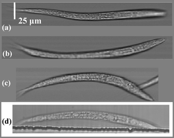 | ||
| Fig. 2 (a)–(c) OFM images of wild-type C. elegans at the first larval stage; white bar = 25 µm. (d) Conventional microscope image (40× objective lens) of a similar nematode. | ||
The OFM can be treated as a set of parallel near-field scanning optical microscopes (NSOM),9 operating in the collection mode. The resolution limit of the OFM can be established by measuring the collection mode point spread function (CPSF) of the aperture. The CPSF is defined as the variation in the transmission through the aperture from a point source that is laterally scanned across the aperture. In other words, the vertical axis of a CPSF plot is the transmission and the horizontal axis is the lateral displacement of the point source from the aperture's center (e.g.Fig. 3(b)). The resolution of the OFM for a target at any given plane above the aperture array is given by the width of the CPSF for that plane. As the CPSF broadens with increasing height from the aperture array, the resolving power of the OFM, likewise, deteriorates with increasing height. The exact relationship between resolution and height is discussed in detail elsewhere.10 The resolution limit of a given OFM is equal to the width of the CPSF at zero height from the aperture array. Practically, this resolution is only attained for parts of the targets that are in near field with the aperture array.
 | ||
| Fig. 3 (a) Illustration of the experimental scheme. A NSOM tip is raster scanned over an aperture. The transmission signal is collected through a relay microscope. D = 600 nm; x: the lateral distance between the NSOM tip and the aperture center. (b) The CPSF extracted from the acquired NSOM image (inset). | ||
We experimentally measured the near-field CPSF of the apertures used in our prototype with a transmission mode NSOM (Alpha-SNOM, WITec Gmbh). The experimental setup is illustrated in Fig. 3(a) where the NSOM tip was taken as a pseudo point object. The illumination is provided by a red laser diode (λ = 650 nm, 30 mW). Given that the NSOM tip is approximately 80 nm wide and the aperture is 600 nm in diameter, the approximation of the NSOM tip as a point source is reasonable. Fig. 3(b) shows the measured CPSF profile of the OFM prototype. Based on the measurements of 8 different apertures, the resolution limit of our OFM prototype is calculated to be 490 ± 40 nm (Sparrow's criterion11). However, we note that to reach this resolution during the imaging process, the target will have to be in contact with the aperture array plane and the CCD pixel acquisition time will have to be sufficiently short. We also note that, as the resolution limit of the OFM is fundamentally constrained by the aperture size, OFM with resolution that is better than the diffraction limit can, in principle, be realized by using smaller apertures.
In addition to nematode research, the OFM can also be applied to image individual cells, e.g. blood cells and cells in suspensions. In such applications, fine microfluidic control based on electrokinetics may be required to ensure uniform translation of the cells with minimal rotation. Fluorescence imaging capability can also be added into the OFM platform by fabricating planar filters8 between the aperture array and the sensor array.
Finally, the simplicity and compact nature of the OFM systems lead to the possibility of fabricating multiple OFMs onto a single microfluidic chip. The microscopes can be used in parallel to increase imaging throughput or linked in serial to perform sequential imaging of the same targets. The latter configuration can be used to perform multispectral imaging of the targets by fabricating a different spectral filter into each OFM unit.
In summary, we presented a new imaging method—the optofluidic microscopy technique, that can be used to create on-chip microscope systems. We demonstrated the feasibility of the method and performed imaging of wild-type C. elegans. The acquired OFM images are comparable to that obtained with a microscope (40× objective lens). In addition, we demonstrated a high throughput imaging rate of about 40 worms min−1.
Acknowledgements
We are grateful for the help from Axel Scherer, P. P. Vaidyanathan, Joerg Schilling, Xiquan Cui and James Adleman. We thank Caltech's Molecular Materials Research Center for providing us with the NSOM system. The assistance from Cornell Nanofabrication Facility and Caltech Watson Clean-room is appreciated. This project was funded by DARPA Center for Optofluidic Integration.Notes and references
- T. Thorsen, S. J. Maerkl and S. R. Quake, Science, 2002, 298, 580–584 CrossRef CAS
.
- P. C. H. Li and D. J. Harrison, Anal. Chem., 1997, 69, 1564–1568 CrossRef CAS
- A. Daridon, M. Sequeira, G. Pennarun-Thomas, H. Dirac, J. P. Krog, P. Gravesen, J. Lichtenberg, D. Diamond, E. Verpoorte and N. F. de Rooij, Sens. Actuators, B, 2001, 76, 235–243 CrossRef
- M. M. Wang, E. Tu, D. E. Raymond, J. M. Yang, H. C. Zhang, N. Hagen, B. Dees, E. M. Mercer, A. H. Forster, I. Kariv, P. J. Marchand and W. F. Butler, Nat. Biotechnol., 2005, 23, 83–87 CrossRef CAS
- D. Akin, H. B. Li and R. Bashir, Nano Lett., 2004, 4, 257–259 CrossRef CAS
- J. B. Salmon, A. Ajdari, P. Tabeling, L. Servant, D. Talaga and M. Joanicot, Appl. Phys. Lett., 2005, 86
- D. Lange, C. W. Storment, C. A. Conley and G. T. A. Kovacs, Sens. Actuators, B, 2005, 107, 904–914 CrossRef
- M. L. Adams, M. Enzelberger, S. Quake and A. Scherer, Sens. Actuators, A, 2003, 104, 25–31 CrossRef
- B. Hecht, B. Sick, U. P. Wild, V. Deckert, R. Zenobi, O. J. F. Martin and D. W. Pohl, J. Chem. Phys., 2000, 112, 7761–7774 CrossRef CAS
-
X. Heng, X. Cui, D. W. Knapp, J. Wu, Z. Yaqoob, E. J. McDowell, D. Psaltis and C. Yang, Opt. Express, 2006, in preparation
-
T. R. Corle and G. S. Kino, Confocal Scanning Optical Microscopy and Related Imaging Systems, Academic Press, San Diego, 1996 Search PubMed
Footnote |
| † Current address: Sibley School of Mechanical and Aerospace Engineering, Cornell University, Ithaca, NY, 14853, USA. |
| This journal is © The Royal Society of Chemistry 2006 |