Structural and optoelectronic properties of C60 rods obtained via a rapid synthesis route†
Yizheng
Jin
a,
Richard J.
Curry
*a,
Jeremy
Sloan
a,
Ross A.
Hatton
a,
Lok Cee
Chong
a,
Nicholas
Blanchard
a,
Vlad
Stolojan
a,
Harold W.
Kroto
b and
S. Ravi P.
Silva
a
aAdvanced Technology Institute, School of Electronics and Physical Sciences, University of Surrey, Guildford, Surrey, UK GU2 7XH. E-mail: r.j.curry@surrey.ac.uk; Fax: +44 (0)1483 689404; Tel: +44 (0)1483 682713
bDepartment of Chemistry and Biochemistry, The Florida State University, Tallahassee, Florida 32306-4390, USA
First published on 21st August 2006
Abstract
High purity single crystal C60 rods with uniform dimensions are synthesized by a rapid and facile approach which can be completed over a timescale of typically a few minutes. The morphology of the fullerene product has been characterized in detail by scanning electron microscopy, scanning transmission electron microscopy, and atomic force microscopy, demonstrating that the resulting materials are solid, hexagonal cross-sectioned rods with novel faceted tips. High resolution transmission electron microscopy investigations reveal that the rods are face-centered cubic packed single crystals. Vibrational and electronic spectroscopy studies provide compelling evidence that the rods are a van der Waals solid since the electronic structure of the component C60 molecules is largely preserved. The structures obtained are found to possess novel optoelectronic properties exhibiting low energy absorption not reported in related structures and materials to date. Furthermore significant room temperature photoluminescence is obtained from the C60 rods accompanied by a small blue shift of the spectra which is also observed for the first ‘allowed’ absorption transitions. Given their rapid synthesis, excellent purity, optical and charge transport properties these fullerene structures are expected to be a promising materials for nanoelectronic devices including thin film organic solar cells and photodetectors.
Introduction
Since its discovery by Kroto et al. in 1985,1 molecular C60 has attracted international research attention due to its high symmetry, its novel conjugated π-system, its unique chemical and physical properties and the potential applications of both C60 and related derived materials.2–6 Theoretical predictions and experimental results indicate that crystals formed from C60 are n-type semiconductors with direct bandgaps that can be further tailored via doping techniques.7 The close packing of C60 molecules in the face-centered-cubic (fcc) crystals results in a relatively high electron mobility (∼0.1 cm−2 V−1 s−1) making it attractive as an n-type material for organic transistors.8 The high ionization potential of C60 and the stability of the anion have resulted in its widespread application as an electron acceptor in heterojunction organic solar cells.9–11 A recent electrical conductivity study on a single tube, ca. 300 nm in diameter, formed from C60 also suggests that the fullerene tube has a large photoconductivity under light illumination, which is promising for optical switching applications.12 Fabrication of one-dimensional C60 structures with sub-micron or nanoscale diameters is therefore fundamentally important for future applications.It has been reported that C60 tubes with diameters of 200–300 nm can be generated via a templated ‘dip and dry’ solvent evaporation route.13 However, the use of a template limits the scale of this preparation, and the C60 tubes obtained are polycrystalline, which degrades their optical characteristics. Miyazawa et al. have described a liquid/liquid interfacial precipitation (LLIP) method for the synthesis of sub-micron sized C60 whiskers and tubes,14,15 a method subsequently applied to the synthesis of similar structures formed from C70 and fullerene derivatives such as C60C3H7N.16–20 It was found subsequently that illumination, in particular at wavelengths between 600 and 625 nm, during crystal growth could significantly promote the growth of needle-like C60 crystals.21,22 A drawback of this method is that it can take up to a week to obtain stable C60 whiskers. To solve this problem, Lee et al. designed a silicon microchannel reactor using a Y-shaped mixer which leads to stable interface reactions thereby speeding up the process but results in larger micron size whiskers being formed.23 However, to date, a rapid, efficient and easily scalable method of producing high purity, high quality one dimensional C60 structures with sub-micron dimensions has been lacking.
In this paper, we report a quick one-step method of making high purity single crystal C60 rods with uniform sub-micron dimensions simply by controlled dropwise addition of a C60/toluene solution into an alcohol solvent. Crucially the synthetic procedure is completed within ∼2 minutes and therefore represents a significant advance over previously reported methods.13–15,21,22 The C60 structures formed using this fast liquid/liquid interface precipitation method (FLLIP) have been fully characterized using scanning electron microscopy (SEM), atomic force microscopy (AFM), scanning transmission electron microscopy (STEM), high resolution transmission electron microscopy (HRTEM), Fourier transform infrared spectroscopy (FTIR), Raman spectroscopy (Raman), X-ray photoelectron spectroscopy (XPS), ultra-violet/visible absorption spectroscopy and photoluminescence spectroscopy (PL), yielding detailed information on the structure, bonding, physicochemical and optical properties.
Experimental
C60 (99.5%, Materials & Electrochemical Research Corporation), toluene (HPLC grade, Aldrich) and isopropyl alcohol (IPA, HPLC grade, Aldrich) were used as received.In a typical experiment 2.0 ml 0.30 wt.% C60/toluene solution was dropped into 8.0 ml IPA at room temperature at a desired rate controlled by a syringe pump. The liquid instantly turned brown upon addition of the C60/toluene solution to the IPA, forming a suspension which was allowed to settle. The solid product was separated by filtration (using 50 nm PTFE filter paper) and dried in vacuum.
SEM (FEI, Quanta 200F), AFM (Digital Instruments, Dimension 3100), STEM (FEI, Quanta 200F), HRTEM (JEOL 3000F, operated at 300 keV), FTIR (Perkin Elmer Spectrum One, KBr disk), Raman (Renishaw 2000 system, 782 nm excitation), XPS, absorption (UV-Vis-NIR, Varian Cary 5000) and PL (514 nm excitation, 60 mW) were used to characterize the fullerene samples. SEM and AFM samples were prepared by depositing a few drops of suspension that contained solid product onto silicon wafers and allowing solvents to evaporate at room temperature. For HRTEM investigations, the suspension was sonicated for 10 min before being transferred to a holey carbon coated copper grid. In order to observe cross-sections of the rods directly, resin was added to the sample and allowed to infiltrate for 24 h prior to observation to achieve resin polymerization. Thin sections were cut on a Leica Ultracut Ultramicrotome and collected onto bare nickel TEM support grids. A manual grinding technique with the aid of a pestle and mortar was also utilized to obtain fragments of rods for HRTEM characterization. XPS experiments were carried out in an Omicron Multiprobe UHV Chamber with a base pressure in the range of 10−9 mbar using Mg Kα radiation from a VG XR3E2 twin anode source coupled to an Omicron HA125 analyzer. The operating power of the X-ray source was set to 300 W. The pass energy was 50 eV for the survey spectra and 20 eV for the higher resolution spectra.
Results and discussion
The brown product was initially characterized by SEM using an electron beam energy of 15 keV. As shown in Fig. 1a, the sample consists principally of an abundance of straight rods, generally orientated with the principle axis arranged parallel to the plane of the substrate. Based on a histogram of 100 randomly selected rods (Fig. 1b), the lengths of the rods are in the range 4–8 µm. The diameters of the rods are typically 200–800 nm, with a small fraction of rods having diameters less than 200 nm. SEM and TEM observations reveal that individual rods possess very uniform diameters along their entire length and the aspect ratios (length/diameter) are >10. Although small particles tens of nanometers in diameter are occasionally observed distributed among the C60 rods, this is rare and in general the surfaces of the rods are clean.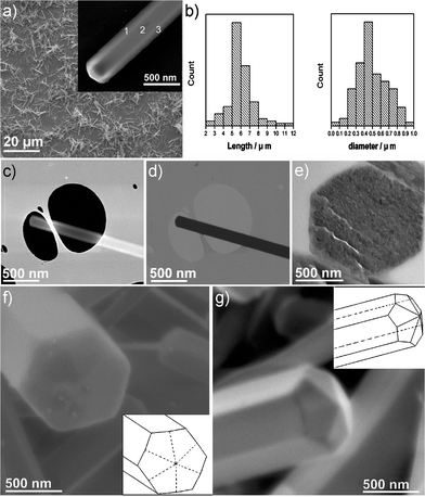 | ||
| Fig. 1 a) SEM image of C60 rods. Inset is a SEM image of a single C60 rod. Note the contrast differences between areas 1 and 2 or areas 2 and 3. b) Histogram showing the respective distributions of lengths (left) and diameters (right) of 100 randomly selected C60 rods. c) SEM image and d) corresponding STEM image of one C60 rod. The latter reveals that the C60 rod is solid rather than hollow (cf. a) inset and c)). e) Representative TEM image of the sample sliced by microtome, confirming the solid hexagonal cross section. f) SEM image showing the end profile of an individual C60 rod. Inset is the schematic structural diagram. g) SEM image recorded from the tip of a second C60 rod showing the faceting more clearly. The inset structural diagram indicates that this faceted tip is symmetrically composed of six rhombuses individually bisected by the faceting present in the body of the C60 rod. | ||
Two features are apparent when imaging single C60 rods by SEM (Fig. 1a inset). Firstly, the tips of the rods are not flat, but are slightly pointed and exhibit faceting relative to an unfaceted or “flat” tip surface. In addition, a significant proportion of rods show clear contrast variations across their cross-sections as indicated in Fig. 1a inset. In order to ascertain the ‘solidity’ of the C60 rods they were probed using STEM. A second SEM image is shown in Fig. 1c and shows similar contrast effects to the example inset in Fig. 1a. The corresponding STEM image is shown in Fig. 1d and, in such an image, the contrast is dominated by the thickness cross-section of the needles, indicating that this C60 rod is solid. The microtome technique was also used to obtain thin cross sections of a statistically significant number of rods. Solid hexagonal cross sections can be observed (Fig. 1e), in agreement with the SEM and STEM observations. As the rods are semi-transparent towards electrons having 15 keV kinetic energy, decreasing the electron beam energy to 1 keV greatly increases the surface sensitivity. Fig. 1f clearly shows the faceted morphology of a C60 rod tip with a hexagonal cross-section. The hexagonal morphology is also supported by AFM measurements (ESI,† Fig. S1). Notably the tip of the C60 rod is not a simple hexagonal pyramid but consists of six facets which are apparently bisected by the longitudinal C60 rod facets as shown in the schematic drawing inset in Fig. 1f. A second example of this unique type of tip morphology, together with its corresponding schematic depiction (inset), is shown in Fig. 1g. The morphology of the tip is similar to that of the multiply twinned fullerene particles.24,25
The detailed crystal structure of the C60 rods has been characterized by HRTEM. Fig. 2a shows a TEM image of a rod, ca. 380 nm in diameter, that had been subjected to 10 min sonication. Note that no breakage or other structural damage can be observed in the TEM image of this sample indicating a significant degree of stability towards this form of physical disturbance. The rods are typically more than 200 nm in thickness, and it is therefore difficult to obtain high quality HRTEM images with reasonable contrast from the solid bodies of the rods. HRTEM images were therefore obtained from the thinnest regions of the rods as indicated in Fig. 2a and c. Two images from the edge of the main body of the C60 rod and from the tip are shown in Fig. 2b and d, respectively. Two sets of spots in a fast Fourier transform (FFT) pattern of Fig. 2b can be indexed as (111) and (220) planes of fcc packing of pristine C60 crystals. The orientation of this FFT with respect to the C60 rod indicates that the growth direction of the rod is parallel to [110]. TEM investigation on the tip (Fig. 2c and d) of the C60 rod suggests that the C60 rod exhibits a long range order throughout the entire tip which is consistent with the results indicated in Fig. 1. The lattice fringes shown in Fig. 2d, indexed as {111} planes of fcc packing C60 crystals, are parallel to edge of the tip which is likely to be the sector boundary. This stacking configuration is coincident with previous reports on multiply twinned fullerene particles.24,25 All the fragments examined in our experiments, which were obtained by the mechanical grinding technique, were similarly well crystallized and presented long-range order. When manipulated using the probes of a nano-manipulator the rods were found to be brittle and invariably cleaved along the same plane of the applied bending force. This is good further evidence for a single crystal structure. To sum up, the present observations indicate that the rods are solid fcc crystals with hexagonal cross-sections and symmetrically faceted tips composed of six rhombuses. The overall crystal habit is illustrated in Fig. 2e and f.
![a) TEM image of one C60 rod. b) HRTEM image recorded at the edge the rod (square area in a)). Inset is the FFT pattern. c) TEM image of the tip of one C60 rod. d) HRTEM image of the square area in c). Inset is the FFT pattern. e) Perspective view and f) end-on cross-sectional view indicating the overall habit of the main body of the C60 needle. The crystal growth direction is [110]. The {111} plane is indicated in e).](/image/article/2006/JM/b609074e/b609074e-f2.gif) | ||
| Fig. 2 a) TEM image of one C60 rod. b) HRTEM image recorded at the edge the rod (square area in a)). Inset is the FFT pattern. c) TEM image of the tip of one C60 rod. d) HRTEM image of the square area in c). Inset is the FFT pattern. e) Perspective view and f) end-on cross-sectional view indicating the overall habit of the main body of the C60 needle. The crystal growth direction is [110]. The {111} plane is indicated in e). | ||
The kinetically favoured or chosen direction of crystal growth (parallel to [110] in this case) is presumably the one which incurs the lowest surface free energy in terms of its formation. This is affected by local crystallisation conditions and we have found that by varying these, the obtained crystalline morphology may differ. This is the subject of a further study and we will comment in more detail on this in a future publication. We note that with regard to the work presented here no twinning was observed in any of the observed C60 rods and our results indicate that they are all apparently single crystal.
The FTIR spectrum of fullerene rods is displayed in Fig. 3a. Four peaks located at 527, 576, 1182 and 1429 cm−1 are characteristic of pristine C60 and the absence of any other prominent features confirms that the rods consist primarily of molecular C60. In particular no additional peaks are distinguishable in the spectra of the C60 rods corresponding to the solvents used during our synthesis in contrast to the previously reported silicon microreactor synthesis method.23 The absence of IR features that would be associated with trapped IPA or toluene is an indication of the very high purity of the samples obtained by this rapid preparative technique.
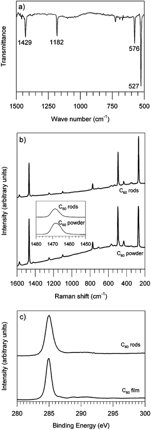 | ||
| Fig. 3 a) FTIR spectra of C60 rods. b) Raman spectra of C60 rods and pristine C60 powder. c) XPS spectra of C60 rods and evaporated C60 film. | ||
Fig. 3b shows the Raman spectrum of C60 rods, which is very similar to that of the pristine C60 powders. The Ag (2) ‘pentagonal pinch’ mode whose peak is located at 1468 cm−1 is known to be sensitive in terms of the intermolecular bonding.26 As displayed in the inset of Fig. 3b, no distinguishable difference of the Ag (2) mode peak can be found between two spectra, which suggests that molecular C60 dominates in the sample and C60 polymerization is not evident.
The molecular nature of the C60 rods is corroborated by the core level electronic spectra measured using XPS. The C1s core-level peak of the C60 rods is shown in Fig. 3c where it is compared with the C1s core-level peak of an ex-situ evaporated C60 film measured on the same instrument. The two spectra show very similar line-shapes, with the main peak attributed to C–C bonds27 lying at 285.0 eV for the rods and 284.9 eV for the evaporated film. Both fitted well to a true Voigt function.28 As can be seen Fig. 3c the main difference is the respective full width at half maximum (FWHM) of the two peaks; the main peak of the evaporated film fitted a synthesized profile with a FWHM of 1.0 eV (at the resolution of the instrument), however the peak of the C60 rod sample required a FWHM of 1.4 eV. This appears to be a significant increase in width and is attributed to the superposition of C1s core-level electrons emitted from the different crystallographic facets of the C60 rods (Fig. 2e). Differences of tenths of electronvolts in the work function of different crystal planes of the same material are common. We found good agreement between our XPS measurements on the evaporated film and the loss structure of the high binding energy tail of the main carbon peak described of Weaver et al.27 (data not shown). The essentially identical peak position and similarity in the high binding energy tail of the spectrum of the rods and the spectrum of the thin film supports the conclusion that they have a common chemical structure.
To further investigate the nature of the C60 rods their electronic structure was probed using optical absorption and photoluminescence spectroscopy. Fig. 4a shows the absorption spectra obtained from a dilute solution of C60, a sublimed thin (90 nm) film of C60, and from C60 rods dispersed in IPA. Intense scattering precluded the measurement of the absorption spectrum of the dry C60 rods. All three spectra have been arbitrarily ‘normalized’ in intensity to the peak at ∼350 nm which corresponds to the first allowed electronic transition in C60. The close resemblance of the prominent absorption peaks at ∼220 nm, ∼265 nm and 340 nm corresponding to allowed intramolecular electronic transitions between the HOMO and LUMO energy levels indicates that the electronic structure of the molecule is largely preserved in both the rods and the film. The absorption of C60 in solution is in close agreement with previous reports exhibiting very weak peaks in the low energy tail at ∼500, 540, 570, 598 and 620 nm assigned to vibrational structure from one or two forbidden electronic transitions (e.g.1Ag to 1F1g).29 Likewise, detailed inspection of the C60 film absorption reveals features at ∼598, 615, 640 and 680 nm similar to previously reported data.29,30 The most intense absorptions in the visible part of the thin film spectra occur at ∼445 nm and ∼500 nm and are attributed to Frenkel and charge transfer excitons respectively.31 Whilst the former is forbidden in the isolated molecule the selection rules for intramolecular transitions are relaxed in the crystal field of the solid and the intensity of the excitonic transition becomes critically dependent on the extent of intermolecular overlap.32 Similarly charge transfer excitations, which result in a final-state hole and electron residing on different C60 molecules, are also characteristic of the condensed phase since to first order approximation they are proportional to the intermolecular overlap integral. The C60 rod spectrum has features common to the spectra of C60 in solution and as a thin polycrystalline film. The solution and C60 rod spectra both exhibit a significant decrease in absorption at ∼435 nm at which there is a local maximum in the C60 film spectrum previously identified as resulting from Frenkel excitonic transitions. Given the crystalline nature of the rods and the polycrystalline nature of the C60 thin film this difference in the absorption spectra might not be expected. It is however important to note that the absorption spectrum of C60 rods in Fig. 4a was obtained for a dilute dispersion of rods in IPA. It is known that crystalline C60 forms solvated structures with many organic solvents on account of its relatively porous structure.17,33 In solvated structures the solid swells to accommodate solvent molecules and so the average intermolecular distance is increased. Since the intensity of Frenkel excitonic transitions which are forbidden in the free molecule is critically dependent on the extent of intermolecular overlap, an increase in intermolecular separation would drastically reduce the intensity of Frenkel excitonic transitions as observed in this case. Conversely, an intense absorption at ∼500 nm in the C60 film, previously attributed to charge transfer exciton transitions, is also present in the C60 rod spectrum with an intensity that is comparable to the first allowed electronic transition. As the intensity of charge transfer excitonic transitions is also dependent on the intermolecular overlap, this is evidence of the condensed phase.
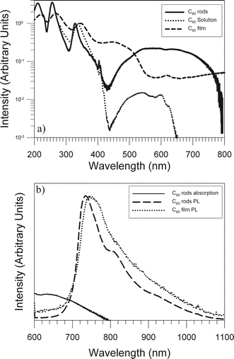 | ||
| Fig. 4 a) Absorption of C60 rods, C60 in solution and a 90 nm C60 sublimed film. b) PL spectra of C60 rods and a thick C60 film (low energy tail of C60 rod absorption also shown). | ||
A proportion of the low energy (>500 nm) absorption that is present in the C60 rod spectrum can be assigned to forbidden Frenkel states with the 0–0 electronic transition occurring at ∼670 nm (1.85 eV).31 The origin of the significant absorption observed in the C60 rod spectrum at wavelengths above 670 nm is therefore unclear. Even at wavelengths above 700 nm (well below the 0–0 electronic transition) the strength of this absorption is still significant and has not previously been observed from C60 single crystals or polycrystalline films. As mentioned above the inability to obtain absorption data from dry C60 rods required the suspension of the rods in IPA which may lead to the inclusion of solvent in the structures modifying the electronic states. This also precluded further measurements in our existing apparatus (e.g. at low temperatures) to gain further information on the origin of this extended absorption. The significantly increased strength of the photoluminescence (see below) obtained from the C60 rods could indicate that the direct absorption into the triplet states maybe allowed through a combination of solvation, inter- and intramolecular effects although this cannot be verified at present.
Also evident within the absorption spectra are slight variations in the position of the peak corresponding to the first allowed electronic transition at ∼350 nm for each of the spectra and also the peaks at ∼220 nm and 265 nm for the thin film and C60 rod spectra. Previous work has shown that following polymerization the first allowed electronic transition is increased in energy by ∼0.1 eV (∼10 nm at 350 nm).29 Whilst a blue shift in the C60 rod spectra as compared to the C60 film is indeed observed, the magnitude of the shift (16 nm) is considerably larger that previously reported. To investigate this discrepancy further and explore the origin of the long wavelength absorption of the C60 rods, PL spectra of the rods dried at room temperature were obtained. The PL spectrum of a thick C60 film (Fig. 4b) is in agreement to that previously reported for C60 originating from the 3F1g to 1Ag phosphorescent transition.29 In both cases the pump wavelength (514 nm) is directly exciting the charge transfer excitonic state present in both samples with similar absorption strength relative to the first allowed electronic transition. The strength of the emission obtained from the C60 rods is however of a significantly higher intensity to that observed from the films under the same excitation conditions. This can be qualitatively observed in Fig. 4b as the level of noise is much reduced in the C60 rod PL spectrum compared to the film. This indicates that Herzberg–Teller coupling between the 3F1g and 1Ag states is stronger in the C60 rod structures and therefore leads to an increase in the intensity of such transitions.29 Such a mechanism could also be responsible for increasing the absorption observed in this wavelength region leading to a substantial overlap between the emission and absorption spectra as observed in Fig. 4b.
This increase in PL intensity is of interest when compared to the effects of bundling on the emission of single-wall carbon nanotubes (CNTs).34 In this case the emission intensity is decreased due to the presence of metallic CNTs. In our C60 rod structures however this mechanism is not available and being formed from identical molecules energy transfer between molecules (leading to a red-shift in PL) is also unlikely. Additionally, our measurements were carried out on ensembles of C60 rods and hence we could not determine if there were any effects relating to the 1-D nature of the structures. If the states from which the PL originates are highly localised we would not expect to observe any significant dependence on rod diameter.
Comparison of the PL spectra of the C60 rods and film shows a slight blue shift of the former similar to that observed in the absorption spectra. If polymerization of the rods had occurred a 0.05 eV (5 nm) red shift of the PL to lower energy would be expected29 ruling out the possibility of polymerization and in agreement with previous results (Fig. 3b). Since the HOMO–LUMO transitions in molecular semiconductors are very sensitive to the proximity of adjacent molecules, we suggest that the blue shift in both the absorption and PL spectra of the C60 rods as compared to the thin films is due to a slight distortion of the fcc structure, such as a fractionally reduced unit cell dimension along the growth direction of the rods. Investigations aimed at testing this hypothesis are under way and will be reported in a subsequent publication.
We also note that all PL studies were carried out in air at ambient temperatures (∼300 K) over a period of days. No degradation of the emission was observed over these time periods and hence we believe the stability of the C60 rods to be suitable for the development of devices.
Conclusions
In conclusion we have demonstrated a rapid and facile method of synthesizing high purity C60 rods of quite uniform dimensions. The rods have hexagonal cross-sectioned prism like morphologies with symmetrically faceted tips composed of six rhombuses. Electron microscopy shows that the rods are fcc packing single crystals with growth directions parallel to [110]. Detailed examination of the C60 rods by a range of techniques including electronic and vibrational spectroscopy have provided compelling evidence that the C60 rods are a molecular crystalline solid and are not polymerized. The approach described herein provides a rapid, simple, and efficient technique for the production of pure C60 rods which can be readily scaled up. The optical properties of the rods obtained demonstrate room temperature photoluminescence and a unique extended absorption at low energies. Coupled with the excellent charge transport characteristics of C60 single crystals and the sub-micron scale infrastructures these materials show significant promise for applications in nanoscale electronic devices including organic solar cells and photodetectors.Acknowledgements
This work was supported by the UK Engineering and Physical Sciences Research Council (EPSRC) Portfolio Research Grant Scheme. We are grateful Dr David Cox and Mr Oliver Wilhelmi for assistance with SEM and STEM facilities. We thank Mr Nanditha Dissanayake for providing the evaporated C60 film.References
- H. W. Kroto, J. R. Heath, S. C. Obrien, R. F. Curl and R. E. Smalley, Nature, 1985, 318(6042), 162–163 CrossRef CAS.
- H. W. Kroto, A. W. Allaf and S. P. Balm, Chem. Rev., 1991, 91(6), 1213–1235 CrossRef CAS.
- C. A. Mirkin and W. B. Caldwell, Tetrahedron, 1996, 52(14), 5113–5130 CrossRef CAS.
- R. Taylor and D. R. M. Walton, Nature, 1993, 363(6431), 685–693 CrossRef CAS.
- F. Diederich, L. Isaacs and D. Philp, Chem. Soc. Rev., 1994, 23(4), 243–255 RSC.
- T. Sakurai, X. D. Wang, Q. K. Xue, Y. Hasegawa, T. Hashizume and H. Shinohara, Prog. Surf. Sci., 1996, 51(4), 263–408 CrossRef CAS.
- W. E. Billups and M. A. Ciufolini, Buckminsterfullerenes. VCH, New York, 1993, p 217 Search PubMed.
- C. D. Dimitrakopoulos and P. R. L. Malenfant, Adv. Mater., 2002, 14, 99–117 CrossRef CAS.
- N. S. Sariciftci, Prog. Quantum Electron., 1995, 19(2), 131–159 CrossRef CAS.
- H. Imahori and Y. Sakata, Adv. Mater., 1997, 9(7), 537–& CAS.
- S. R. Forrest, MRS Bull., 2005, 30, 29–32.
- Y. J. Xing, G. Y. Jing, J. Xu, D. P. Yu, H. B. Liu and Y. L. Li, Appl. Phys. Lett., 2005, 87(26) Search PubMed.
- H. B. Liu, Y. L. Li, L. Jiang, H. Y. Luo, S. Q. Xiao, H. J. Fang, H. M. Li, D. B. Zhu, D. P. Yu, J. Xu and B. Xiang, J. Am. Chem. Soc., 2002, 124(45), 13370–13371 CrossRef CAS.
- K. Miyazawa, Y. Kuwasaki, A. Obayashi and M. Kuwabara, J. Mater. Res., 2002, 17(1), 83–88 CrossRef CAS.
- K. Miyazawa, Y. Kuwasaki, K. Hamamoto, S. Nagata, A. Obayashi and M. Kuwabara, Surf. Interface Anal., 2003, 35(1), 117–120 CrossRef CAS.
- K. Miyazawa and T. Suga, J. Mater. Res., 2004, 19(11), 3145–3148 CrossRef CAS.
- J. Minato and K. Miyazawa, Carbon, 2005, 43(14), 2837–2841 CrossRef CAS.
- K. Miyazawa, K. Hamamoto, S. Nagata and T. Suga, J. Mater. Res., 2003, 18(5), 1096–1103 CrossRef CAS.
- K. Miyazawa, T. Mashino and T. Suga, J. Mater. Res., 2003, 18(11), 2730–2735 CrossRef CAS.
- K. Miyazawa, J. Am. Ceram. Soc., 2002, 85(5), 1297–1299 CAS.
- K. Kobayashi, M. Tachibana and K. Kojima, J. Cryst. Growth, 2005, 274(3–4), 617–621 CrossRef CAS.
- M. Tachibana, K. Kobayashi, T. Uchida, K. Kojima, M. Tanimura and K. Miyazawa, Chem. Phys. Lett., 2003, 374(3–4), 279–285 CrossRef CAS.
- S. H. Lee, K. Miyazawa and R. Maeda, Carbon, 2005, 43(4), 887–889 CrossRef CAS.
- B. Pauwels, D. Bernaerts, S. Amelinckx, G. Van Tendeloo, J. Joutsensaari and E. I. Kauppinen, J. Cryst. Growth, 1999, 200(1–2), 126–136 CrossRef CAS.
- B. W. vandeWaal, J. Cryst. Growth, 1996, 158(1–2), 153–165 CrossRef CAS.
- A. M. Rao, P. Zhou, K. A. Wang, G. T. Hager, J. M. Holden, Y. Wang, W. T. Lee, X. X. Bi, P. C. Eklund, D. S. Cornett, M. A. Duncan and I. J. Amster, Science, 1993, 259(5097), 955–957 CAS.
- J. H. Weaver, J. L. Martins, T. Komeda, Y. Chen, T. R. Ohno, G. H. Kroll, N. Troullier, R. E. Haufler and R. E. Smalley, Phys. Rev. Lett., 1991, 66(13), 1741–1744 CrossRef CAS.
- J. A. Leiro, M. H. Heinonen, T. Laiho and I. G. Batirev, J. Electron Spectrosc. Relat. Phenom., 2003, 128(2–3), 205–213 CrossRef CAS.
- Y. Wang, J. M. Holden, A. M. Rao, P. C. Eklund, U. D. Venkateswaran, D. Eastwood, R. L. Lidberg, G. Dresselhaus and M. S. Dresselhaus, Phys. Rev. B, 1995, 51(7), 4547–4556 CrossRef CAS.
- C. Reber, L. Yee, J. McKiernan, J. I. Zink, R. S. Williams, W. M. Tong, D. A. A. Ohlberg, R. L. Whetten and F. Diederich, J. Phys. Chem., 1991, 95(6), 2127–2129 CrossRef CAS.
- M. Knupfer and J. Fink, Phys. Rev. B, 1999, 60(15), 10731–10734 CrossRef CAS.
- S. Kazaoui, N. Minami, Y. Tanabe, H. J. Byrne, A. Eilmes and P. Petelenz, Phys. Rev. B, 1998, 58(12), 7689–7700 CrossRef CAS.
- M. V. Korobov, E. B. Stukalin, A. L. Mirakyan, I. S. Neretin, Y. L. Slovokhotov, A. V. Dzyabchenko, A. I. Ancharov and B. P. Tolochko, Carbon, 2003, 41, 2743–2755 CrossRef CAS.
- M. J. O'Connell, S. M. Bachilo, C. B. Huffman, V. C. Moore, M. S. Strano, E. H. Haroz, K. L. Rialon, P. J. Boul, W. H. Noon, C. Kittrell, J. Ma, R. H. Hauge, R. B. Weisman and R. E. Smalley, Science, 2002, 297, 593–596 CrossRef CAS.
Footnote |
| † Electronic supplementary information (ESI) available: an AFM image of a single C60 rod (Fig. S1). See DOI: 10.1039/b609074e |
| This journal is © The Royal Society of Chemistry 2006 |