Electrochemically deposited Pd islands on an organic surface: the presence of Coulomb blockade in STM I(V) curves at room temperature
O.
Shekhah
a,
C.
Busse
a,
A.
Bashir
a,
F.
Turcu
b,
X.
Yin
a,
P.
Cyganik†
a,
A.
Birkner
a,
W.
Schuhmann
b and
Ch.
Wöll
a
aLehrstuhl für Physikalische Chemie I, Ruhr-Universität Bochum, D-44780, Bochum, Germany
bAnalytische Chemie – Elektroanalytik & Sensorik, Ruhr-Universität Bochum, D-44780, Bochum, Germany
First published on 5th June 2006
Abstract
Palladium islands with a thickness of a few monolayers were deposited on top of a self-assembled monolayer (SAM) fabricated from 4-mercaptopyridine. In the I(V) curves obtained using the scanning tunneling microscope (STM) clearly the signature of Coulomb blockade is observed, explicitly demonstrating that these islands are coupled to the underlying gold substrate only via a tunneling barrier; this spectroscopic feature also allows to distinguish the palladium islands from similar morphological features present on the gold substrate prior to palladium deposition.
Electronic transport through organic materials is of outstanding scientific and technological interest.1 The key challenge with regard to precisely determining experimentally the transport properties is to reproducibly establish reliable electrical contacts to organic materials and, at the same time, to determine accurate information on the molecular geometry at the metal/molecule junctions. In the past years a number of different strategies have been employed for the formation of such contacts. The most straightforward approach is clearly to take a conductive (e.g. a metal) substrate, deposit a molecular layer on the top of the substrate by organic molecular beam deposition (OMBD)2 and then to form a second contact on top of the organic layer by metal evaporation. Although this method is very often used aiming at the fabrication of organic electronic devices like organic field effect transistors, this approach severely suffers from the fact that the atoms will diffuse into the organic adlayer. Thus metal organic contacts are obtained which are poorly defined and where the first layers of the organic material are potentially doped with metal atoms.3
By far the largest body of previous work on forming well-defined metallic contacts to organic materials is based on self-assembled monolayers (SAMs).4 SAMs are prepared by immersing a gold substrate into a solution of appropriate organic thiols, which then bind with the gold surface by forming a stable covalent thiolate bond. For SAMs the substrate can thus serve as the bottom electrode. The evaporation of a metal on top of the SAM does not yield a well-defined top electrode; detailed previous work has shown also in this case typically a diffusion of the metal atoms down to the substrate.5–7 In recent work by Tai et al.8 this diffusion of the metal atoms down to the substrate could be avoided by previously polymerizing the SAM. However, in this case no electrical characterization of the metal deposits has been carried out. To our knowledge previous successful fabrications of well-defined metal/organic/metal were based on attaching preformed metal particles originating either from a cluster beam,9 by chemical methods,10 or by pulse laser deposition.11 In these approaches the electrical characterization of the metal electrode was carried out by contacting the metal with a tip of a scanning tunneling microscope (STM) or the electrically conducting tip of a contact-probe atomic force microscope (CP-AFM).10
Recently, a major breakthrough has been achieved with regard to forming well-defined metal deposits on top of a SAM by using a two-step electrochemical procedure. This approach, which has been developed by Kolb and coworkers,12–14 starts by immersing a gold single crystal into a solution of 4,4′-dithiodipyridine. This leads to the formation of a 4-mercaptopyridine (4-MP) SAM. In a second step Pd2+ ions are deposited on top of the SAM by immersing the SAM into a PdSO4 solution. After removing the sample from this solution the Pd2+ ions adsorbed on top of the pyridine SAM are reduced using standard electrochemical methods.12,14 After palladium deposition the presence of Pd atoms at the very top of the SAM can be demonstrated using angular dependent X-ray photoelectron spectroscopy (XPS)14 and ion scattering spectroscopy (ISS).15 The XPS data clearly prove the presence of Pd0 on top of the SAM.
It seems to be surprising at first sight that Pd0 and not Pd2+ is observed in the XPS since after removing the samples from the electrochemical solution the palladium atoms have been in ambient conditions for short times. Since palladium is known to be rather reactive with regard to O2 this contact with air should yield palladium oxide and, correspondingly, Pd2+ should be seen in the XPS data. This apparent discrepancy has been explained by the particular electronic structure of the palladium islands present on top of the SAM which do not resemble that of bulk palladium and thus also exhibit different chemical activities.16
Previous attempts to manufacture top metal contacts on SAMs fabricated using electrochemical methods have all suffered from the fact that when using one-step electrochemical processes very often metallic short cuts were formed between the deposited metal and the substrate by mushroom structures formed between the metal and the top contact.17,18 Therefore, the ultimate proof that the Pd islands, deposited using the two-step method described above, are really insulating and do not exhibit short cuts to the substrate has to be provided by contacting these Pd islands and studying their electrical properties.
In the present work we have used the tip of an STM operated under ultra-high vacuum conditions (UHV) to demonstrate that the electrical conductivity of the palladium islands is indeed different from that of the substrate and also from Au islands which are formed during the adsorption process of aromatic thiols on gold substrates. To our knowledge this is the first case where room temperature Coulomb blockade has been observed for electrochemically deposited metal particles.
Experimental
The preparation procedure is in principle the same as that described in ref. 12. In brief, it consists of immersing the freshly annealed Au(111) single crystal for 5 min into an aqueous solution of 20 μM 4,4′-dithiodipyridine (AldrithiolTM-4, Aldrich, 98%). This leads to formation of the 4-mercaptopyridine (4-MP) SAM. The SAM-modified Au(111) single crystal was then thoroughly rinsed with water and immersed for 15 min in 0.1 mM PdSO4 (Aldrich, 99.99%) + 0.1 M H2SO4 (Sigma-Aldrich, 99.99%), to allow Pd2+ adsorption/complexation with the SAM. After rinsing again with water, the Au(111) single crystal was transferred to the electrochemical cell, containing a 0.1 M H2SO4 solution.
The Pd-loaded sample was contacted with the electrolyte in the electrochemical cell at +0.7 V to prevent the unintentional reduction of the adsorbed Pd2+. The potential scan was started from +0.6 V to −0.2 V with a scan rate of 5 mV s−1 in cathodic direction for electro-reduction of the surface-bound metal ions. All potentials are quoted vs. a Ag/AgCl, KCl (3 M) reference electrode. The cyclic voltammograms were recorded with an EcoChemie Autolab PG20 potentiostat. STM measurements in air and in UHV were performed using a JEOL JSPM-4210 and a JEOL JSPM-4500S instrument, respectively. Typically, tunneling voltages around U = 1.0 V were applied (with respect to the sample) and currents around I = 0.1 nA were obtained. STM data were acquired at room temperature.
Results and discussion
In Fig. 1 we show the cyclic voltammogram obtained for the Pd2+-loaded 4-MP SAM-Au(111) in 0.1 M H2SO4. The first cycle shows a cathodic current peak at ≈−0.045 V, which is absent in the second cycle. This indicates that an irreversible process has taken place on the surface, which is the reduction of the adsorbed Pd2+ to Pd0 and that the reduction process was complete.12
 | ||
| Fig. 1 Cyclic voltammetry curve of Pd-loaded 4-MP SAM on Au(111) surface in 0.1 M H2SO4. The first (solid line) and second (dotted line) cycles are shown. Scan rate: 5 mV s−1. | ||
In Fig. 2a we show a typical STM image recorded for a 4-MP SAM deposited on a gold single crystal before Pd deposition. Note that already at this stage many nanometer-sized Au islands are observed on the surface, which are formed during the SAM formation process. These Au islands have an average diameter of l ≈ 10 nm and the same height (h ≈ 0.24 nm) as atomic steps on the Au(111)-substrate. For most organothiols studied before depressions (or etch-pits) are observed instead of these islands19,20 but for organothiols containing an aromatic unit directly connected to the thiol group, the observation of these adatom islands is rather common.21,22 The formation process of these islands is not yet completely understood. Note, however, that the top of these Au adatom-islands is also covered by the SAM (see Fig. 2a and the schematic diagram in Fig. 3).
 | ||
| Fig. 2 (a) STM image of 4-MP SAM on Au(111) single crystal (5 min in solution of 20 μM 4,4′-dithiodipyridine), recorded in air, scan width 130 × 130 nm. (b) STM image after Pd deposition (15 min in 0.1 mM PdSO4 solution) obtained in air. Scan width 130 × 130 nm. The height-scale is the same for both images. (c) Profiles across (a) (black) and (b) (red) as indicated by the respective white lines. | ||
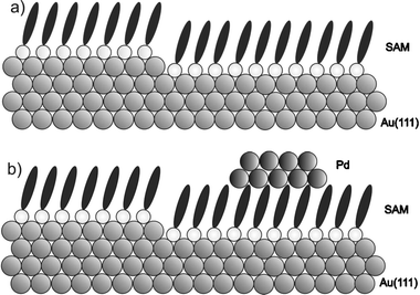 | ||
| Fig. 3 A schematic diagram of (a) the 4-MP SAM islands formed on the Au(111) surface before Pd deposition. (b) Pd islands formed on top of the SAMs after Pd deposition. | ||
Fig. 2b shows an STM image recorded after Pd deposition. Clearly, now a second type of higher islands is seen in the data. The height of these structures shows a rather broad distribution centered at h = 1.5 nm. Their average diameter amounts to l = 18 nm. We identify these structures as palladium islands with a thickness of a few atomic layers (see Fig. 3), in accordance with the previous work.13–15
In order to determine the electrical characteristics of the adsorbed islands we have recorded I(V) curves by using the STM tip as a second electrode. These measurements were carried out in the current imaging tunneling spectroscopy mode (CITS), where along with each pixel of a topographic image an I(V)-spectrum is measured. This allows an exact correlation between I(V) curves and the sample location. Furthermore, by averaging over several I(V) spectra obtained over equivalent positions of the sample, the signal-to-noise ratio of the curves can be drastically enhanced.
A topographic image obtained in CITS mode consisting of 128 × 128 pixels is shown in Fig. 4a. Here, one of the higher Pd islands is seen in the lower left. Fig. 4c shows a typical I(V) curve recorded for the SAM-covered surface (filled circles) and on top of the particle in the lower left (red squares), both curves are obtained by averaging >50 single point spectra. For comparison, the I(V) curve of a bare gold surface is also shown (open circles). It is obvious that the I(V) curves recorded on top of the island reveals significant differences and shows the typical signature of a Coulomb blockade with a threshold value of Ec/e = 0.5 V.10,23
 | ||
| Fig. 4 (a) STM image of Pd-covered sample taken under UHV-conditions, scan width 25 nm × 25 nm, Utunnel = 1 V, Itunnel = 0.1 A. Inset: profile along the white line. (b) Current image of the area shown in (a), tunnel voltage 0.75 V. (c) Model of the double barrier tunnel junction with associated equivalence circuit. (d) I(V) curves (averaged over > 50 single spectra) obtained on the bright particle in the lower left corner (red squares) and somewhere on the unstructured area of the substrate (filled circles), blue line indicates voltage at which the current image (Fig. 4b) was taken. The vertical arrows indicate the width of the Coulomb blockade. For comparison, an I(V) curve taken on the clean Au(111) is shown (open circles). | ||
Fig. 4b shows a current map where the tunneling current measured at a voltage of 0.76 eV (blue line in Fig. 4d) has been used for contrast generation. One can clearly see that the low current is typical for the Pd islands whereas the islands within the SAM (which were already present before Pd deposition, compare with Fig. 3) do not show up when using this contrast mechanism due to the fact that their conductivity is identical to that of the SAM on the flat substrate.
The electrostatic charging energy Ec of the Pd island shown in Fig. 4b amounts to Ec ≈ 0.5 eV (compare Fig. 4d), yielding a tunneling capacitance Ct = e2/2 Ec = 0.15 aF (see Fig. 4c). A crude estimate of the overall geometric capacitance (Ct = C1 + C2) can be obtained by treating both C1 and C2 as parallel plate capacitors with an area A and a separation of d between the plates (C = ε0ε A/d). The area A can be obtained from the STM images and is assumed to be the same for C1 and C2. For the length of the gap between Au(111) and Pd islands we assume d1 ≈ 1 nm (length of 4 MP-molecule plus S–Au and N–Pd separation). The separation d2 was not measured in this experiments but we can assume it to be comparable to d1.24 Neglecting the (unknown) ε of 4 MP, this approximation yields Ct = 0.35 aF for the particle depicted in Fig. 4b (diameter, l ≈ 4.9 nm), the same order of magnitude as obtained from the charging energy Ec. Measurements on other Pd islands with different sizes yielded slightly different charging energies, as expected.24
Conclusions
In conclusion, we have deposited palladium islands on top of a self-assembled monolayer made from a pyridine-terminated organothiols following a previously established procedure by Kolb and coworkers.12,13 The presence of a Coulomb-blockade in the STM I(V) curves recorded at room temperature clearly demonstrates that these palladium islands are insulated from the metal substrate. This characterization using STM spectroscopy also allows distinguishing the palladium island from the gold adatom islands, which are present on the gold-SAM surface prior to palladium deposition.
Acknowledgements
This work was supported by the German DFG (SPP 1121, WO 464/17/3). We are grateful for helpful advice from D. Kolb and V. Ivanova (Ulm) and we would like to acknowledge helpful discussions with J. König (Bochum).References
- C. Joachim, J. K. Gimzewski and A. Aviram, Nature, 2000, 408, 541 CrossRef CAS.
- G. Witte and C. Wöll, J. Mater. Res., 2004, 19, 1889–1916 CrossRef CAS.
- A. C. Dürr, F. Schreiber, M. Kelsch, H. D. Carstanjen and H. Dosch, Adv. Mater., 2002, 14, 961 CAS.
- J. C. Love, L. A. Estroff, J. K. Kriebel, R. G. Nuzzo and G. M. Whitesides, Chem. Rev., 2005, 105, 1103–1169 CrossRef CAS.
- A. W. Czanderna and D. R. Jung, Crit. Rev. Solid State Mater. Sci., 1994, 19, 1 Search PubMed.
- G. L. Fisher, A. V. Walker, A. E. Hooper, T. B. Tighe, K. B. Bahnck, H. T. Skriba, M. D. Reinard, B. C. Haynie, R. Opila, N. Winograd and D. L. Allara, J. Am. Chem. Soc., 2002, 124, 5528 CrossRef CAS.
- A. V. Walker, T. B. Tighe, J. Stapleton, B. C. Haynie, S. Upilli, D. L. Allara and N. Winograd, Appl. Phys. Lett., 2004, 84, 4008 CrossRef CAS.
- Y. Tai, A. Shaporenko, H. Noda, M. Grunze and M. Zharnikov, Adv. Mater., 2005, 17, 745–1749.
- R. P. Andres, T. Bein, M. Dorogi, S. Feng, J. I. Henderson, C. P. Kubiak, W. Mahoney, R. G. Osifchin and R. Reifenberger, Science, 1996, 272, 1323 CrossRef CAS.
- X. D. Cui, A. Primak, X. Zarate, J. Tomfohr, O. F. Sankey, A. L. Moore, T. A. Moore, D. Gust, G. Harris and S. M. Lindsay, Science, 2001, 294, 571 CrossRef CAS.
- E. A. Speets, B. Dordi, B. J. Ravoo, A. Oncel, A.-S. Hallbäck, H. J. W. Zandfliet, B. Poelsema, G. Rijnders, D. H. A. Blank and D. N. Reinhoudt, Small, 2005, 1, 395 Search PubMed.
- T. Baunach, V. Ivanova, D. M. Kolb, H.-G. Boyen, P. Ziemann, M. Büttner and P. Oelhafen, Adv. Mater., 2004, 16, 2024–2028 CrossRef CAS.
- V. Ivanova, T. Baunach and D. M. Kolb, Electrochim. Acta, 2005, 50, 4283–4288 CrossRef CAS.
- M. Manolova, V. Ivanova, D. M. Kolb, H.-G. Boyen, P. Ziemann, M. Büttner, A. Romanyuk and P. Oelhafen, Surf. Sci., 2005, 590, 146–153 CrossRef CAS.
- O. Shekhah, M. Manolova, D. M. Kolb and C. Wöll., to be published.
- J. M. Seminario and J. M. Tour, Ann. N. Y. Acad. Sci., 1998, 852, 68–94 CrossRef CAS.
- I. Thom, G. Hähner and M. Buck, Appl. Phys. Lett., 2005, 87, 024101 CrossRef.
- M. A. Schneeweiss, H. Hagenström, M. J. Esplandiu and D. M. Kolb, Appl. Phys. A: Mater. Sci. Processing, 1999, 69, 537–551 CrossRef CAS.
- K. Edinger, A. Gölzhäuser, K. Demota, C. Wöll and M. Grunze, Langmuir, 1993, 9, 4 CrossRef CAS.
- K. Edinger, M. Grunze and C. Wöll, Ber. Bunsen-Ges. Phys. Chem., 1997, 101, 1811–1815 CAS.
- Q. Jin, J. A. Rodriguez, C. Z. Li, Y. Darici and N. J. Tao, Surf. Sci., 1999, 425, 101 CrossRef CAS.
- G. Yang and G.-Y. Liu, J. Phys. Chem. B, 2003, 107, 8746–8759 CrossRef CAS.
- G. Yang, L. Tan, Y. Yang, S. Chen and G.-Y. Liu, Surf. Sci., 2005, 589, 129 CrossRef CAS.
- C. Busse, A. Bashir, O. Shekhah, A. Birkner, X. Yin, F. Turcu, W. Schuhmann and C. Wöll, 2006, to be published.
Footnote |
| † Permanent address: Smoluchowski Institute of Physics, Jagiellonian University, Krakow, Poland. |
| This journal is © the Owner Societies 2006 |