Can scanning tunnelling spectroscopy measure the density of states of semiconductor quantum dots?
Peter
Liljeroth
*a,
Lucian
Jdira
b,
Karin
Overgaag
a,
Bruno
Grandidier
c,
Sylvia
Speller
b and
Daniël
Vanmaekelbergh
a
aCondensed Matter and Interfaces, Debye Institute, University of Utrecht, P.O. Box 80000, 3508TA, Utrecht, The Netherlands. E-mail: P.Liljeroth@phys.uu.nl; Fax: +31 30 253 2403
bInstitute for Molecules and Materials, Radboud University Nijmegen, P.O. Box 9010, 6500 GL, Nijmegen, The Netherlands
cInstitut d’Electronique, de Microélectronique et de Nanotechnologie, Département ISEN, 41 bd Vauban, 59046, Lille Cedex, France
First published on 2nd June 2006
Abstract
Molecules, supramolecular structures and semiconductor nanocrystals are increasingly used as the active components in prototype opto-electrical devices with miniaturized dimensions and novel functions. Therefore, there is a strong need to measure the electronic structure of such single, individual nano-objects. Here, we explore the potential of scanning tunnelling spectroscopy to obtain quantitative information on the energy levels and Coulomb interactions of semiconductor quantum dots. We discuss the conditions under which shell-tunnelling, shell-filling and bipolar spectroscopy can be performed, and illustrate this with spectra acquired on individual CdSe and PbSe quantum dots. We conclude that quantitative information on the energy levels and Coulomb interactions can be obtained if the physics of the tip/quantum dot/substrate double-barrier tunnel junction is well understood.
Introduction
Structures with dimensions in the nanometre range such as organic molecules, supramolecular aggregates and inorganic nanocrystals (semiconductor quantum dots (QDs)) are used increasingly as the active component in miniaturized prototype optical and electrical devices.1–6 Since the function of such devices is determined by the electronic structure of the active components, there is a need to measure the density of electronic states in detail. Optical techniques, such as absorption and luminescence spectroscopy, have been used extensively for this purpose.7 However, optical spectroscopy probes electronic transitions between two levels of the molecule or QD subject to certain selection rules. Hence, not all energy levels of the system are reflected in the optical resonances. In addition, the spatial resolution of optical spectroscopy is limited to one fourth of the wavelength of light (typically 100–400 nm): it is usually not possible to probe a single nano-object, except in the special case of a two-dimensional system with strong dilution of the molecules or QDs.8–11In contrast, scanning tunnelling microscopy (STM) and spectroscopy (STS) make it possible to address electrically a single nano-object. In addition, selection rules usually do not play a role in resonant electron tunnelling between a metallic system (the tip) and the nano-object (molecule or QD). In the past, it has been shown that STS is extremely useful in detecting the energy levels of molecules, metallic clusters and semiconductor QDs.12–25 While we will focus on semiconductor QDs, the concepts of tunnelling spectroscopy have also been demonstrated with molecules and metallic clusters.21,25–28 Tunnelling spectroscopy on these systems is based on resonant tunnelling across a double-barrier tunnel junction (Fig. 1): the nano-object is attached to a substrate, and the tip of the STM is placed above the nano-object. In order to be able to study the properties of an essentially isolated object, it is required that the electronic coupling to the substrate and STM tip is weak. The current I between the tip and the substrate is then the result of subsequent tunnelling of electrons (holes) from the tip to the object and object to the substrate, or vice versa. When the Fermi level of the tip or the substrate aligns with one of the energy levels of the nano-object, a tunnelling channel opens resulting in a stepwise increase in the measured current and a peak in the tunnelling conductance, dI/dVbias. The setup shown in Fig. 1 is characterized by the tunnelling rates into, Γin, and out of, Γout, the QD (resistances Rtip/QD and RQD/substrate in the equivalent circuit shown in Fig. 1a) and the capacitances of the junctions.13,15,17 The ratio Γin/Γout will determine the number of additional electrons (holes) in the nano-object at a given bias voltage. In the limiting case Γin ≪ Γout, i.e. shell-tunnelling spectroscopy, electrons (holes) tunnel through the nano-object one-by-one and electron–electron interactions do not occur (Fig. 1b).15 In this case, the peaks in the tunnelling spectrum directly reflect the density of states of the object. Γin can be increased by bringing the STM tip closer to the nano-object. When Γin is comparable to or higher than Γout, the degeneracy of the levels is lifted due to interactions between the carriers accumulating in the nano-object (Fig. 1c), i.e. partial shell-filling spectroscopy.17 This results in additional resonances in the tunnelling spectrum. From measurements of spectra with variable Γin, it is, in principle, possible to obtain information on both the single-electron electronic structure and the electron–electron Coulomb interaction energies.
 | ||
| Fig. 1 Schematics of (a) the equivalent circuit of the double-barrier tunnelling junction, (b) shell-tunnelling and (c) shell-filling spectroscopy. | ||
The relative capacitances of both barriers determine the potential distribution in the double-barrier tunnel junction; this is important if quantitative information is to be extracted from the tunnelling spectroscopy experiments. In addition, a nearly symmetric potential distribution can give rise to more complicated tunnelling schemes leading to bipolar transport, i.e. tunnelling through the same energy level of the QD at both negative and positive bias. This type of transport has been very recently observed in molecular assemblies.29–31
Considering the complexity of the double-barrier tunnel junction, one may ask if it is possible to derive quantitative information on the electronic structure of molecules and QDs from tunnelling spectroscopy experiments. In this work, we discuss a number of effects that are directly related to both the relative capacitances and the electronic transparency of the two barriers in the junction. With spectra acquired on semiconductor QDs as examples, we show that quantitative information can be obtained if the junction is understood. We also show that scanning tunnelling spectroscopy is a very versatile technique and that systematically changing the ratio of both capacitances or tunnelling rates across the barriers can be used to extract additional information on the single-particle energy levels and charge interactions. Although all our illustrations are based on semiconductor QDs, we emphasize that several of our results should also hold for other systems, such as molecules and clusters.
Experimental
Colloidal nanocrystals with a high degree of control over size, shape and surface chemistry can be routinely prepared using the so-called hot-injection solvothermal synthesis route.7,32–34 CdSe nanocrystals capped with trioctylphosphine oxide (TOPO) and hexadecylamine (HDA) and PbSe nanocrystals capped with oleic acid were prepared by standard methods.32,35–37 These dots are nearly spherical and have a size dispersion of 5–10%. The surface of the nanocrystals is passivated by organic ligands; prior to the STM sample preparation, the ligand shell of the as-synthesized nanocrystals was exchanged to shorter, more labile molecules such as hexylamine or pyridine. This greatly enhanced the stability of the nanocrystals under STM imaging. A flame-annealed Au(111) substrate with a self-assembled hexanedithiol monolayer was immersed in a dispersion of colloidal QDs for a few minutes. This leads to stable attachment of isolated QDs and the formation of small aggregates of a few nanocrystals. The nanocrystal coverage on the substrate can be controlled by the QD concentration in the solution and/or the immersion time.The scanning tunnelling microscopy work was performed at 5 K in a home-built cryogenic STM with cut Pt/Ir tips (measurements on CdSe nanocrystals) or in a commercial ultra-high vacuum low-temperature STM (Omicron LT-STM) with etched W tips (PbSe measurements). Tunnelling spectra were acquired at 5 K by placing the STM tip above the centre of an isolated dot well-separated from neighbouring nanocrystals and disconnecting the feedback loop. The tunnelling current I was then measured as a function of the tip–substrate potential difference (bias) Vbias. Tunnelling conductance dI/dVbias was obtained either by digitally filtering and differentiating the experimental I–Vbias curve or by a direct measurement using a lock-in amplifier (typically rms modulation 6 mV at 1 kHz). Typically, a large number (∼100 for each set-point current) of curves were acquired above a single dot and checked for their reproducibility. The I–V curves were reproducible, although discrete shifts of the curves along the voltage axis were observed in some cases. The reason for this could be the trapping of a charge in the surroundings of the dot that acts as a local “gate” and leads to a shift of the measured spectrum.
Results and discussion
Shell-tunnelling spectroscopy
Fig. 2 shows a typical shell-tunnelling spectrum of an isolated CdSe nanocrystal with a diameter of 5 nm. This spectrum was measured at a low set-point current, i.e. with the tip relatively far from the nanocrystal. The tip–QD junction is controlled via the STM feedback settings while the barrier between QD and Au(111) substrate is fixed and is due to the hexanedithiol layer. We observe a series of peaks of increasing intensity on the positive (negative) bias corresponding to electron (hole) tunnelling through the discrete conduction (valence) energy levels. The shell-tunnelling conditions can be confirmed by varying the set-point current, i.e. the ratio of Γin to Γout.17 We observe that within a range of set-point currents, the peak positions are not affected, only the peak intensity is increased by decreasing tip–QD separation (increasing set-point current). Semiconductor QDs are the experimental realization of the text-book example of the quantum mechanical particle-in-a-box problem. The peaks correspond to discrete levels which can be labelled by the symmetry of the wave function of the single-electron energy levels.38,39 The energy separations of the levels are in agreement with pseudo-potential and tight-binding calculations, confirming our assignment of the tunnelling resonances.15,17 In the shell-tunnelling regime, the zero-conductivity gap, ΔVSTM, is related to the energies of the first conduction, ESe, and first valence level, ESh, as ηΔVSTM = ESe − ESh + ΣSe + ΣSh, where η is the fraction of the bias voltage that drops between the tip and the QD (see below) and ΣSe (ΣSh) the polarization (charging) energy of an electron (hole) present in an s-type orbital. This energy depends on the dielectric mismatch between the nanocrystal core and its surroundings and can be estimated given the effective dielectric constants.39–41 The zero-conductivity gap can also be correlated with the optical gap, ΔEopt: ηΔVSTM = ΔEopt + Je–h, where Je–h is the electron–hole attraction energy.17,39–41 | ||
| Fig. 2 (a) Shell-tunnelling spectrum of a 5 nm diameter CdSe nanocrystal. The tunnelling resonances corresponding to the quantum confined, discrete energy levels are indicated by labels referring to the symmetry of the envelope wave function. The inset shows the Se and Pe tunnelling resonances (black line) and calculation based on a simple tunnelling model as outlined in the text (grey line). The measurement parameters were: stabilization bias of 2.5 V and set-point of 60 pA. (b) Schematic showing the bias dependence of the tunnelling barrier height. At higher bias, the effective barrier height between the tip and the QD is increased for resonant tunnelling into the discrete energy level of the QD. This can lead to negative conductance on the high-energy side of the resonance, as observed here at Vbias = 1.6 and 1.9 V. | ||
Based on a simple picture of the shell-tunnelling regime shown in Fig. 1, it might be expected that the peak heights are proportional to the degeneracy of the energy levels. After all, the peaks are due to opening of tunnelling channels and it seems logical that degenerate levels should correspond to more channels and consequently, higher peak amplitude. However, experimental evidence does not confirm this expectation. We observe the ratio of Pe to Se peak heights to vary between 1 and 1.5, while a ratio of 3 is expected on the basis of degeneracy. More detailed considerations show that the symmetry of the orbitals has to be taken into account, in analogy with chemical bonding. As can be seen from the schematic shown in Fig. 3, within the triply degenerate P-level, only the pz orbital has significant overlap with the tip and thus gives rise to resonant transmission. The transmission coefficient of electron tunnelling from the tip to the px and py orbitals is likely to be very small at the centre of the nanocrystal. In addition, the overlap integral of px and py orbitals with the substrate (neglecting atomistic details) is zero. In conclusion, the P resonance in the measured spectrum probably corresponds to only tunnelling through the Pz state. The slight difference in the peak heights between the Se and Pe resonance can be due to either the lower effective tunnelling barrier height or higher overlap of the Pz state with the tip and substrate as compared to the Se level. Similar reasoning can be applied to the orbitals at higher energy (de, fe).
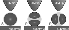 | ||
| Fig. 3 Schematic illustration of the overlap of the different QD orbitals with the tip and the substrate. | ||
Typically, negative differential resistance (NDR) can be observed at positive bias, in particular for resonances corresponding to tunnelling through the S and P conduction levels. This effect can be understood readily by considering a simple tunnelling model. In the shell-tunnelling regime, at 0 K, and assuming constant density of states for the tip, the current for electron tunnelling from the tip into the QD is proportional to42,43
 | (1) |
| T(E,Vbias) ∝ exp (−kz0 (ϕ − E + eVbias/2)1/2) | (2) |
For a quantitative estimate of the energy levels of the QD based on the measured tunnelling spectra, the distribution of the bias in the double-barrier tunnelling junction has to be taken into account. We can calculate this by solving the Laplace equation for a realistic tip–dot–substrate geometry as shown in Fig. 4. Typically, it is found that η = (Vdot − Vtip)/Vbias is close to 0.7 for dot sizes between 3 and 7 nm, and realistic tip-to-dot and dot-to-substrate distances (tip–dot 5–15 Å and dot–substrate 5 Å). There is a weak dependence on the tip radius of curvature, for example, for a 3 nm CdSe nanocrystal with 1 nm tip-to-dot and 0.5 nm dot-to-substrate distances, we obtain η = 0.70, 0.67, and 0.64 for rtip = 5, 10, and 15 nm, respectively. Experimentally, rtip can be estimated from the apparent lateral size of the nanocrystals due to tip convolution and it is usually ∼10 nm. The potential distribution in the double-barrier tunnel junction induces a linear shift of the tunnelling resonances to higher biases: the bias voltage at the resonances is related to the energy levels, Ei, through ηVbias = Ei + Σi. Once the potential distribution has been accounted for, tunnelling spectroscopy in the shell-tunnelling regime can yield quantitative information on the energy level structure of QDs.15,17,22,24,44
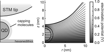 | ||
| Fig. 4 Calculated potential distribution in the STM tip/QD/substrate double-barrier tunnel junction based on the solution of the Laplace equation. Dielectric constants 10.2 CdSe and 2 for organics. Tip radius 10 nm. | ||
Shell-filling spectroscopy
Beyond a certain set-point current, qualitative changes occur in the spectra. Compared to the spectrum shown in Fig. 2, the number of resonances increases considerably indicating that the relative rates of tunnelling into and out of the QD are nearly equal. Fig. 5 shows two tunnelling spectra of a 3 nm CdSe nanocrystal under such conditions, i.e. in the partial shell-filling regime (black lines). This means that electrons accumulate in the dot and the degeneracy of the energy levels is lifted by electron–electron interactions which is reflected in the spectra by the appearance of new peaks. In the partial shell-filling regime, the spectra can be rather complicated and for the assignment of the peaks, a master equation model is used. | ||
| Fig. 5 (a) Partial shell-filling spectroscopy: two examples of tunnelling spectra with a 3 nm diameter CdSe QD (black lines). Stabilization bias 2.5 V and set-point current of 240 pA (lower spectrum) and 380 pA (upper spectrum). The origin of the tunnelling resonances at positive bias marked by (a)–(e) is explained in the text. The two measured spectra exhibit a discrete shift of all the energy levels. The simulated spectra based on the master equation approach with the parameters given in the text are shown in grey lines. The lower panels show schematics of tunnelling of electrons through the Se conduction level both at (b) positive and (c) negative bias. In the schematic diagrams, the position of the Fermi level of the substrate is kept constant. | ||
We will first discuss the resonances at positive bias marked by letters (a)–(e) in Fig. 5a. These peaks are due to electron tunnelling through conduction levels (Fig. 5b) where the degeneracy of the Se and Pe levels is lifted due to electron–electron interactions. We use a master equation approach,44,45 which gives the probability of having n electrons and p holes in the QD, σn,p. These together with the tunnelling rates of electrons and holes across the tip-to-dot and dot-to-substrate junctions allow the calculation of the tunnelling current. The grey lines in Fig. 5 give the simulated tunnelling spectra which were obtained with Γin/Γout = 4 and η = 0.61. The difference between the two spectra is only a shift of all the QD energy levels with respect to the Fermi energy of the tip and the substrate.
The ratio of the tunnelling rates in and out of the QD determines the degree of shell-filling, i.e. electron accumulation. With the help of the master equation simulations, we are able to assign the peaks at positive bias to the following tunnelling transitions: (a) S0P0 → S1P0, (b) S1P0 → S2P0, (c) S0P0 → S0P1, (d) S1P0 → S1P1, and (e) S2P0 → S2P1. For example, peak (c) corresponds to an excited state with electron tunnelling through the P-level with no electrons on the S-level. The peaks (a) and (b) are separated by the electron–electron interaction energy, which in the present case was 120 meV. In contrast to our measurements on CdSe QDs, Millo et al. report complete shell-filling conditions in the spectroscopy of colloidal InAs nanocrystals: the Se and Pe levels are recorded as a doublet and sextuplet, respectively.12,46,47
Simultaneous electron and hole transport
A rather symmetric potential distribution over both barriers (η → 0.5) can lead to simultaneous electron and hole transport. For example, at negative bias, it is possible that before the tip Fermi level reaches resonance with the first valence level of QD, the substrate Fermi level becomes resonant with a conduction band level resulting in tunnelling through this level (Fig. 5c). Then the first tunnelling resonance at both negative and positive bias corresponds to electron tunnelling through the same orbital of the QD. If electrons tunnel on both sides of the zero-conductivity gap, the following relation holds44 | (3) |
 | (4) |
The situation of electron tunnelling on both sides of the gap is illustrated in Fig. 5a. If we compare the upper experimental spectrum with the lower one in Fig. 5a (black lines), it is clear that all the peaks at positive bias have shifted to lower energies whereas the first peak at negative bias has shifted in the other direction. These shifts are due to a sudden change in ESe − EF resulting probably from trapping of an electron in the surroundings of the dot. This charge can act as a local “gate” and lead to a shift of the entire spectrum. Under “normal” conditions, both conduction and valence level peaks shift in the same direction. This confirms that the first resonance at negative bias is actually due to tunnelling through the conduction levels as schematically shown in Fig. 5c. Further support for this assignment of the tunnelling resonances is provided by the master equation approach. The calculated spectra (Fig. 5a, grey lines) agree very nicely with the experiments; the only difference in the parameters between the upper and lower calculated spectra is a constant shift of all the energy levels w.r.t. the Fermi level.
It is also possible to realise transport of holes through the filled valence levels on both sides of the zero-conductivity gap. This requires QDs with high-lying levels, so that the first valence level is close to the Fermi levels of the tip and substrate. PbSe is such a material and Fig. 6a shows an example of tunnelling spectroscopy of PbSe nanocrystals with a diameter of ca. 4 nm (black lines). The top trace is measured on a nanocrystal that exhibits a “normal” spectrum with the conduction levels appearing at positive bias and the valence levels at negative bias, which is the most common case observed experimentally.16 In contrast, the lower spectrum shows distinctly different behaviour: the first valence level is close to zero bias. At positive bias, there is a series of equally spaced peaks of the same amplitude. We observe this type of spectra in a significant minority of cases. These spectra can be understood by considering the schematics shown in Fig. 6b and c. At negative bias, we observe normal hole tunnelling through the valence levels. These processes occur in the shell-tunnelling regime, i.e. the tunnelling rate between the tip and the QD is much smaller than the tunnelling rate between the dot and the substrate. At positive bias, we again observe hole tunnelling through the valence levels. However, now the rate limiting step is the tunnelling between the tip and the QD and hence, holes are accumulating in the QD.
 | ||
| Fig. 6 (a) Tunnelling spectroscopy of 4 nm diameter PbSe nanocrystals (black lines) and a calculated tunnelling spectrum (grey line). Stabilization settings in both experimental spectra were bias 1.2 V and set-point 100 pA. The lower panels show schematics of tunnelling of holes through the Sh valence level both at (b) negative and (c) positive bias. In the schematic diagrams, the position of the Fermi level of the substrate is kept constant. | ||
The reason for the difference between the two experimental spectra shown in Fig. 6a (black lines) is that nanocrystals on the surface can have different binding geometries that may alter the voltage distribution over them. In addition, the local environment (trapped charges etc.) can induce an electrostatic shift of all the energy levels that can vary from QD to QD. Variation of these factors can lead to the conditions required for hole tunnelling at both negative and positive bias: relatively symmetric potential distribution over the double-barrier tunnel junction and high-lying energy levels with the first valence level close to the Fermi levels of the tip and substrate.
PbSe has an interesting band structure with the fundamental gap at the L-point of the Brillouin zone.16,48,49 This means that all the quantum-confined levels have a four-fold higher multiplicity than, for example, in CdSe. Moreover, in contrast to II-VI semiconductors, the effective masses of electron and holes are nearly equal which results in symmetric conduction and valence levels with the two lowest levels having S and P envelope symmetry, respectively. The symmetric levels scheme is reflected in the measured tunnelling spectrum (Fig 6a, top spectrum). The higher multiplicity of the energy levels of PbSe is confirmed by our observation of six equally spaced resonances, indicating subsequent filling of the first, 8-fold degenerate hole level (Fig. 6b lower spectrum). Based on the simulations (Fig. 6a, grey line), we can extract a hole–hole interaction energy of 120 meV. The ratio of the tunnelling rates used in the simulation was Γin : Γout = 1 : 10, confirming the shell-tunnelling conditions. The strong increase of conductance at higher positive bias (Vbias > 1 V) is due to concomitant electron tunnelling through the conduction levels with hole transport. Under such conditions, electrically induced exciton luminescence from a single QD can be expected.
Conclusions
Using colloidal semiconductor QDs as examples, we have shown how scanning tunnelling spectroscopy can be used to extract information on the electronic density of states and Coulomb interactions of individual nano-objects. Obtaining quantitative information requires that the properties of the double-barrier tunnel junction are understood in detail. The relative tunnelling rates into and out of the QD determines the degree of carrier accumulation in the nano-object, and allow us to switch between shell-tunnelling and shell-filling regimes. If the potential distribution over the two barriers is symmetric, it is possible to observe bipolar transport, i.e. tunnelling through the same energy levels at both positive and negative bias. In addition, electron and hole transport through the QD can occur simultaneously at higher bias, which may give rise to single-photon emission.Acknowledgements
Financial support through the European Union (NANOSPECTRA, HPRH-CT-2001-00320) and the Netherlands Foundation for Fundamental Research on Matter (FOM) is gratefully acknowledged. We are thankful to Arjan Houtepen, Celso de Mello Donegá and Stephen G. Hickey for the nanocrystal samples used in this study.References
- D. L. Klein, R. Roth, A. K. L. Lim, A. P. Alivisatos and P. L. McEuen, Nature, 1997, 389, 699 CrossRef CAS
.
- H. Park, J. Park, A. K. L. Lim, E. H. Anderson, A. P. Alivisatos and P. L. McEuen, Nature, 2000, 407, 58 CAS
- J. Park, A. N. Pasupathy, J. I. Goldsmith, C. Chang, Y. Yaish, J. R. Petta, M. Rinkoski, J. P. Sethna, H. D. Abruna, P. L. McEuen and D. C. Ralph, Nature, 2002, 417, 722 CrossRef CAS
- W. J. Liang, M. P. Shores, M. Bockrath, J. R. Long and H. Park, Nature, 2002, 417, 725 CrossRef CAS
- S. J. Tans, A. R. M. Verschueren and C. Dekker, Nature, 1998, 393, 49 CrossRef CAS
- H. S. J. van der Zant, Y. V. Kervennic, M. Poot, K. O’Neill, Z. de Groot, J. M. Thijssen, H. B. Heersche, N. Stuhr-Hansen, T. Bjornholm, D. Vanmaekelbergh, C. A. van Walree and L. W. Jenneskens, Faraday Discuss., 2006, 131, 347 RSC
- C. B. Murray, C. R. Kagan and M. G. Bawendi, Annu. Rev. Mater. Sci., 2000, 30, 545 Search PubMed
- S. Empedocles and M. Bawendi, Acc. Chem. Res., 1999, 32, 389 CrossRef CAS
- M. Nirmal, B. O. Dabbousi, M. G. Bawendi, J. J. Macklin, J. K. Trautman, T. D. Harris and L. E. Brus, Nature, 1996, 383, 802 CrossRef CAS
- W. van Sark, P. Frederix, D. J. Van den Heuvel, H. C. Gerritsen, A. A. Bol, J. N. J. van Lingen, C. de Mello Donegá and A. Meijerink, J. Phys. Chem. B, 2001, 105, 8281 CrossRef CAS
- M. Bayer, P. Hawrylak, K. Hinzer, S. Fafard, M. Korkusinski, Z. R. Wasilewski, O. Stern and A. Forchel, Science, 2001, 291, 451 CrossRef CAS
- U. Banin, Y. W. Cao, D. Katz and O. Millo, Nature, 1999, 400, 542 CrossRef CAS
- U. Banin and O. Millo, Annu. Rev. Phys. Chem., 2003, 54, 465 CrossRef CAS
- D. Steiner, T. Mokari, U. Banin and O. Millo, Phys. Rev. Lett., 2005, 95, 056805 CrossRef CAS
- E. P. A. M. Bakkers, Z. Hens, A. Zunger, A. Franceschetti, L. P. Kouwenhoven, L. Gurevich and D. Vanmaekelbergh, Nano Lett., 2001, 1, 551 CrossRef CAS
- P. Liljeroth, P. A. Zeijlmans van Emmichoven, S. G. Hickey, H. Weller, B. Grandidier, G. Allan and D. Vanmaekelbergh, Phys. Rev. Lett., 2005, 95, 086801 CrossRef
- L. Jdira, P. Liljeroth, E. Stoffels, D. Vanmaekelbergh and S. Speller, Phys. Rev. B, 2006, 73, 115305
- J. Repp, G. Meyer, F. E. Olsson and M. Persson, Science, 2004, 305, 493 CrossRef CAS
- J. Repp, G. Meyer, S. M. Stojkovic, A. Gourdon and C. Joachim, Phys. Rev. Lett., 2005, 94, 026803 CrossRef
- G. V. Nazin, X. H. Qiu and W. Ho, Science, 2003, 302, 77 CrossRef CAS
- G. V. Nazin, S. W. Wu and W. Ho, Proc. Natl. Acad. Sci. U. S. A., 2005, 102, 8832 CrossRef CAS
- T. Maltezopoulos, A. Bolz, C. Meyer, C. Heyn, W. Hansen, M. Morgenstern and R. Wiesendanger, Phys. Rev. Lett., 2003, 91, 196804 CrossRef
- B. J. LeRoy, S. G. Lemay, J. Kong and C. Dekker, Nature, 2004, 432, 371 CrossRef CAS
- B. J. LeRoy, J. Kong, V. K. Pahilwani, C. Dekker and S. G. Lemay, Phys. Rev. B, 2005, 72, 075413 CrossRef
- H. Zhang, G. Schmid and U. Hartmann, Nano Lett., 2003, 3, 305 CrossRef CAS
- R. Wilkins, E. Ben-Jacob and R. C. Jaklevic, Phys. Rev. Lett., 1989, 63, 801 CrossRef CAS
- J. G. A. Dubois, E. N. G. Verheijen, J. W. Gerritsen and H. van Kempen, Phys. Rev. B, 1993, 48, 11260 CrossRef CAS
- J. W. Gerritsen, S. E. Shafranjuk, E. J. G. Boon, G. Schmid and H. van Kempen, Europhys. Lett., 1996, 33, 279 CrossRef
- G. V. Nazin, X. H. Qiu and W. Ho, J. Chem. Phys., 2005, 122, 181105 CrossRef CAS
- N. A. Pradhan, N. Liu, C. Silien and W. Ho, Nano Lett., 2005, 5, 55 CrossRef CAS
- S. W. Wu, G. V. Nazin, X. Chen, X. H. Qiu and W. Ho, Phys. Rev. Lett., 2004, 93, 236802 CrossRef CAS
- C. B. Murray, D. J. Norris and M. G. Bawendi, J. Am. Chem. Soc., 1993, 115, 8706 CrossRef CAS
- C. de Mello Donegá, P. Liljeroth and D. Vanmaekelbergh, Small, 2005, 1, 1152 Search PubMed
- L. Manna, E. C. Scher and A. P. Alivisatos, J. Am. Chem. Soc., 2000, 122, 12700 CrossRef CAS
- C. de Mello Donegá, S. G. Hickey, S. F. Wuister, D. Vanmaekelbergh and A. Meijerink, J. Phys. Chem. B, 2003, 107, 489 CrossRef
- C. B. Murray, S. Sun, W. Gaschler, H. Doyle, T. A. Betley and C. R. Kagan, IBM J. Res. Dev., 2001, 45, 47 CrossRef CAS
- A. J. Houtepen, R. Koole, D. Vanmaekelbergh, J. Meeldijk and S. G. Hickey, J. Am. Chem. Soc., 2006, 128, 6792 CrossRef CAS
- D. J. Norris and M. G. Bawendi, Phys. Rev. B, 1996, 53, 16338 CrossRef CAS
-
C. Delerue and M. Lannoo, Nanostructures: Theory and Modelling, Springer-Verlag, Berlin, 2004 Search PubMed
- A. Franceschetti, A. Williamson and A. Zunger, J. Phys. Chem. B, 2000, 104, 3398 CrossRef CAS
- A. Franceschetti and A. Zunger, Phys. Rev. B, 2000, 62, 2614 CrossRef CAS
- N. D. Lang, Phys. Rev. B, 1986, 34, 5947 CrossRef
- M. Grobis, A. Wachowiak, R. Yamachika and M. F. Crommie, Appl. Phys. Lett., 2005, 86, 204102 CrossRef
- Y. M. Niquet, C. Delerue, G. Allan and M. Lannoo, Phys. Rev. B, 2002, 65, 165334 CrossRef
- D. V. Averin, A. N. Korotkov and K. K. Likharev, Phys. Rev. B, 1991, 44, 6199 CrossRef
- O. Millo, D. Katz, Y. W. Cao and U. Banin, Phys. Rev. B, 2000, 61, 16773 CrossRef CAS
- O. Millo, D. Katz, Y. W. Cao and U. Banin, Phys. Rev. Lett., 2001, 86, 5751 CrossRef CAS
- F. W. Wise, Acc. Chem. Res., 2000, 33, 773 CrossRef CAS
- G. Allan and C. Delerue, Phys. Rev. B, 2004, 70, 245321 CrossRef
| This journal is © the Owner Societies 2006 |