Single-molecule electrical studies on a 7 nm long molecular wire
Geoffrey J.
Ashwell
*a,
Barbara
Urasinska
a,
Changsheng
Wang
b,
Martin R.
Bryce
b,
Iain
Grace
c and
Colin J.
Lambert
c
aThe Nanomaterials Group, School of Chemistry, University of Wales, Bangor, Deiniol Street, Bangor, Gwynedd, UK LL55 2UW. E-mail: g.j.ashwell@bangor.ac.uk
bDepartment of Chemistry, University of Durham, Durham, UK DH1 3LE. E-mail: m.r.bryce@durham.ac.uk
cDepartment of Physics, Lancaster University, Lancaster, UK LA1 4YB. E-mail: c.lambert@lancaster.ac.uk
First published on 26th October 2006
Abstract
A self-assembled arylene–ethynylene molecular wire with a rigid 7 nm long backbone exhibits symmetrical current–voltage (I–V) characteristics and a single-molecule current of 0.35 ± 0.05 nA at 0.3 V; these data are supported by theoretical calculations.
Current research on molecular electronics focuses upon materials that act as diodes,1 switches2,3 and wires4,5 as well as innovative techniques and test-bed structures to contact single molecules and ultra-thin films. These include molecule-inserted nanopores,6 nanowires7,8 break junctions9,10 and crossed-wire geometries in which a monolayer is assembled on one of the wires and contact is magnetically induced via a deflection current in the other.11 There are also recent reports of optical lithographic techniques to produce nanoscale electrode structures for the post-fabrication self-assembly of functionalised nanoparticles12 and molecular wires of precisely defined length.13 These approaches provide a means to overcome the miniaturisation threshold of silicon devices but, despite this, molecule electronics is still in its infancy and considerable effort is required for the design and synthesis of appropriate materials and the development of reliable non-invasive contacting techniques for test-bed characterisation.
In this work, we report the single-molecule electronic properties of a 7 nm long arylene–ethynylene wire (Fig. 1). Its self-assembling precursor, which was synthesised at the University of Durham,14 has an almost linear backbone with hexyloxy side-chains to ensure its solubility, incorporates 9-[di(4-pyridyl)methylene]fluorene and 9-fluorenone moieties to impart electron-accepting characteristics despite being separated by weak dialkoxyphenyl donors, and has cyanoethyl-protected thiol end groups. Monolayers were formed by immersing gold-coated substrates in a tetrahydrofuran solution of the precursor (0.1 mg cm−3) to which sodium methoxide was added to facilitate removal of the protecting groups. Formation of the self-assembled monolayer (SAM) was monitored from the frequency changes following deposition on gold-coated 10 MHz quartz crystals and thorough rinsing with tetrahydrofuran to remove physisorbed material. The frequency became constant after ca. 0.5 h (cf. 4 h in the absence of sodium methoxide) and areas derived from a Sauerbrey analysis15 of the data saturate to ca. 1.3 nm2 molecule−1 both with and without the deprotecting agent. The value is inconsistent with areas calculated from the van der Waals dimensions of the molecular wire but can be explained by partial overlap of these highly tilted molecules in the SAM.
 | ||
| Fig. 1 Molecular structure of the 7 nm long arylene–ethynylene molecular wire. | ||
X-Ray photoelectron spectroscopy confirms the self-assembly: a doublet at 162.1 and 163.5 eV (S 2p1/2 and S 2p3/2) is characteristic of the binding energy of the gold thiolate link and another at 163.7 and 164.6 eV corresponds to the surface based terminal thiol group. Evidence is also provided by the UV/visible spectrum of the SAM on platinum-coated glass: it exhibits a peak at ca. 400 nm when corrected for absorbance of the substrate and mimics the solution spectrum, albeit throughout the limited investigated range (Fig. 2). The absorption band is not shifted, unlike those of many other SAMs, and this probably arises from the conjugated backbones being effectively isolated by hexyloxy side-chains.
 | ||
| Fig. 2 UV/visible spectrum of the self-assembled molecular wire and an outline (broken line) of the solution spectrum where λmax = 400 nm in chloroform. | ||
SAMs of the molecular wire on gold-coated highly oriented pyrolytic graphite (HOPG) were investigated using a MultiMode scanning tunnelling microscope with a Nanoscope IV controller (Veeco Instruments, Cambridge). The SAM was imaged using the STM and, for I–V characterisation, the gold probe was landed at distinct surface features distant from grain boundaries. In each case, the SAMs were investigated at several locations across the surface and the I–V data averaged from multiple scans at each of these sites. They exhibit symmetrical I–V characteristics as expected for symmetrical wire-like molecules located between gold contacts (Fig. 3). We note that to land the probe, the set point current and voltage have little or no effect on the profile of the I–V curves but affect the magnitude of the tunnelling current by influencing the distance between probe and surface. This is demonstrated by other SAMs5 and is a common feature from STM studies on other unreported wire-like molecules in this series.
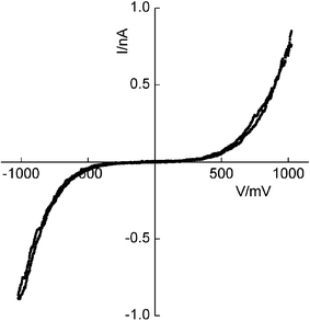 | ||
| Fig. 3 I–V characteristics of the molecular wire deposited as a SAM on gold-coated HOPG and contacted by a gold probe with a set-point current of 0.3 nA and sample bias of 30 mV. The designated polarity relates to the substrate electrode. | ||
Using the method of Haiss et al.,16 single-molecule STM studies were performed by monitoring the current as a function of time at locations across the SAM with the gold probe located at a fixed height and within contacting distance of the surface to chemisorb the thiol-terminated wires. The molecules spontaneously adsorb and desorb with abrupt changes in the tunnelling current (Fig. 4). Each adsorption/desorption event persists for ca. 10 to 300 ms with almost 50% of all current jumps within the range 0.35 ± 0.05 nA for a surface bias of 0.3 V. It is attributed to the single-molecule current and therefore, adsorption via a single thiolate link to the gold probe. Significantly, thirteen of the ninety-nine recorded events exhibit current jumps of 0.65 ± 0.05 nA which is almost double the aforementioned value and probably corresponds to the probe contacting two molecules. There is also tentative evidence of higher multiples with two events centred about 1.05 nA and another centred about 1.45 nA (Fig. 5), these being indicative of three and four-molecule contacts. However, these events correspond to only 3% of the total and we note that the histogram reveals a single high-current event that does not approximate to an integer multiple of the single-molecule value.
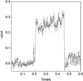 | ||
| Fig. 4 Current jump with the gold STM probe located at a fixed height above the SAM with a sample bias of 0.3 V. The increased current, which is attributed to adsorption of the terminal thiol group to the gold probe, persists for ca. 260 ms in this case and is the longest recorded event. | ||
 | ||
| Fig. 5 Histogram of 99 recorded current jumps at a sample bias of 0.3 V. About 50% (46 events) fall within the range 0.35 ± 0.05 nA with current jumps centred about 0.65 nA (13 events), 1.05 nA (2 events) and 1.45 nA (1 event) approximating to multiples thereof. | ||
The single-molecule current of ca. 0.35 nA at 0.3 V is about six times larger than the value displayed by the I–V plot at this voltage (Fig. 3). It can be explained by the latter being dependent upon the set point conditions which influence the distance between probe and surface whereas the former is independent of the set point current16 as the molecule is chemisorbed by both electrodes. Besides, we note that the upper limiting current exhibited by I–V curves of thiol-terminated molecules approaches the corresponding single-molecule value obtained from the current jump method as the set point conditions are altered to minimise the gap between surface and probe.
In further studies, the electron-accepting 9-[di(4-pyridyl)methyl-ene]fluorene unit has been chemically modified by protonation of both pyridyl units to provide a rectifying junction when combined with an adjacent electron-donating layer of copper phthalocyanine-3,4′,4″,4′″-tetrasulfonate. They exhibit rectification ratios of ca. 20 at ±1 V and the direction of electron flow at forward bias is from the cathode to the electron-accepting layer and from the electron-donating layer to the anode.
We now compare the experimental results with a detailed ab initio simulation of electron transport through the non-protonated self-assembled molecule and show that transport is dominated by the presence of Fano resonances near the Fermi energy. To compute the conductance, we use a combination of the DFT code SIESTA17 and a Green's function scattering approach, as encapsulated in the non-equilibrium molecular electronics SMEAGOL18 code. Starting from the relaxed geometry, obtained from SIESTA, the isolated molecule is extended to include the surface layers of gold leads. A mean-field, DFT, tight binding Hamiltonian of the molecule is obtained, from which a scattering matrix and electron transmission coefficient T(E) are computed. For applied voltages up to approximately 2 V, the voltage dependence of T(E) is found to be insignificant and therefore, the I–V characteristic of Fig. 6 can be found by using formula (1) where μL/R = EF ± eV/2.
 | (1) |
 | ||
| Fig. 6 Theoretical I–V behaviour of the molecular wire contacted by gold. | ||
For the computed electron transmission coefficient T(E) shown in Fig. 7 and a Fermi energy indicated by the dotted line, we obtain the following I–V characteristic, which agrees with the shape of the experimental curve of Fig. 3 and, to within a factor of order unity, agrees with the magnitude of the experimental current (jump) at 0.3 V as shown in Fig. 4.
 | ||
| Fig. 7 Zero bias transmission T(E) versus energy E through the 7 nm molecular wire. | ||
For this wire, T(E) exhibits Fano resonances above the Fermi energy, associated with localised states on the substituent groups attached to the fluorene moieties (i.e. the keto oxygen and dipyridylmethylene). The position of these resonances is sensitive to small perturbations on the side group, which could be induced chemically, geometrically or by gating. This opens up the exciting possibility of using these molecular wires as single-molecule sensors.
We acknowledge the Department of Trade and Industry, QinetiQ, EPSRC, the MCRTN ‘RTNNANO’ and the Royal Society/Wolfson Foundation for support.
Notes and references
- G. J. Ashwell, B. Urasinska and W. D. Tyrrell, Phys. Chem. Chem. Phys., 2006, 8, 3314 RSC.
- E. H. van Dijk, D. J. T. Myles, M. H. van der Veen and J. C. Hummelen, Org. Lett., 2006, 8, 2333 CrossRef CAS.
- A. R. Pease, J. O. Jeppesen, J. F. Stoddart, Y. Luo, C. P. Collier and J. R. Heath, Acc. Chem. Res., 2001, 34, 433 CrossRef CAS.
- J. M. Tour, Acc. Chem. Res., 2000, 33, 791 CrossRef CAS.
- G. J. Ashwell, W. D. Tyrrell, B. Urasinska, C. Wang and M. R. Bryce, Chem. Commun., 2006, 1640 RSC.
- M. A. Reed, J. Chen, A. M. Rawlett, D. W. Price and J. M. Tour, Appl. Phys. Lett., 2001, 78, 3735 CrossRef CAS.
- C. E. Gardner, M. A. Ghanem, J. W. Wilson and D. C. Smith, Anal. Chem., 2006, 78, 951 CrossRef CAS.
- L. T. Cai, H. Skulason, J. G. Kushmerick, S. K. Pollack, J. Naciri, R. Shashidar, D. L. Allara, T. E. Mallouk and T. S. Mayer, J. Phys. Chem. B, 2004, 108, 2827 CrossRef CAS.
- J. Reichert, R. Ochs, D. Beckmann, H. B. Weber, M. Mayor and H. v. Löhneysen, Phys. Rev. Lett., 2002, 88, 176804 CrossRef CAS.
- B. Xu and N. J. Tao, Science, 2003, 301, 1221 CrossRef CAS.
- J. G. Kushmerick, J. Naciri, J. C. Yang and R. Shashidhar, Nano Lett., 2003, 3, 897 CrossRef CAS.
- S. W. Howell, S. M. Dirk, K. Childs, H. Pang, M. Blain, R. J. Simonson, J. M. Tour and D. R. Wheeler, Nanotechnology, 2005, 16, 754 CrossRef CAS.
- G. J. Ashwell, P. Wierzchowiec, C. J. Bartlett and P. D. Buckle, Chem. Commun. Search PubMed , submitted for publication.
- C. Wang, A. S. Batsanov and M. R. Bryce, Faraday Discuss., 2006, 131, 221 RSC.
- G. Sauerbrey, Z. Phys., 1959, 155, 206 CAS.
- W. Haiss, R. J. Nichols, H. van Zalinge, S. J. Higgins, D. Bethell and D. J. Schiffrin, Phys. Chem. Chem. Phys., 2004, 6, 4330 RSC.
- J. M. Soler, E. Artacho, J. D. Gale, A. Garcia, J. Junquera, P. Ordejon and D. Sanchez-Portal, J. Phys.: Condens. Matter, 2002, 14, 2745 CrossRef CAS.
- A. R. Rocha, V. Garcia-Suarez, S. W. Bailey, C. J. Lambert, J. Ferrer and S. Sanvito, Phys. Rev. B, 2006, 73, 085414 CrossRef.
| This journal is © The Royal Society of Chemistry 2006 |