Highly luminescent network films from electrochemical deposition of peripheral carbazole functionalized fluorene oligomer and their applications for light-emitting diodes†
Mao
Li
,
Shi
Tang
,
Fangzhong
Shen
,
Meirong
Liu
,
Weijie
Xie
,
Hong
Xia
,
Linlin
Liu
,
Leilei
Tian
,
Zengqi
Xie
,
Ping
Lu
,
Muddasir
Hanif
,
Dan
Lu
,
Gang
Cheng
and
Yuguang
Ma
*
Key Laboratory for Supramolecular Structure and Materials of Ministry of Education, Jilin University, Changchun, China. E-mail: ygma@jlu.edu.cn; Fax: +86 0431 5168480; Tel: +86 0431 5168480
First published on 11th July 2006
Abstract
Highly luminescent network films on flat indium tin oxide (ITO) substrates are prepared by electropolymerization using an electroactive and fluorescent compound as precursor; the LEDs prepared using these films as a light emitting layer achieve the maximum luminance and external quantum efficiency of 4224 cd/m2 and 0.72%, respectively, which demonstrates that electrochemical synthesis can be a new route to construct the highly luminescent films.
Generally, conjugated polymers prepared by electrochemical synthesis exhibit electrical conductivity,1–4 but weak fluorescence. This is due to a variety of factors, including structure defects and doped counterions present in electrodeposition (ED) films,5–7 which strongly quench the fluorescence. Though a number of investigations have focused on the electrical and charge transport properties of these ED materials,8–11 very little attention has been given to optimizing the optical properties of the emitting layer for organic light-emitting diodes (OLEDs). Previously, the important electroluminescent polymers, poly(p-phenylene) and poly(p-phenylenevinylene) were electropolymerized using cyclic voltammetry (CV) on indium tin oxide (ITO) substrates for OLEDs, but the device performance was very poor due to the very weak fluorescence of the obtained ED films.8–11 Recently, Advincula and his coworkers12 reported a luminescent thin film of conjugated polymers on a flat conducting substrate using the electropolymerization between pendant electroactive carbazole units in a polyfluorene precursor. The large difference in the oxidation potential between polyfluorene and the carbazole unit ensures the electropolymerization of the pendant carbazole groups without affecting the polymer backbone. The fluorescence from these ED films was observed, but the emission exhibited the low energy band at 530 nm and seemed not very strong likely due to the aggregation of the polyfluorene chain and structural defects, such as ketonic and charge doped species.6
In this paper, we report the preparation of highly luminescent network films by electrodeposition of peripheral carbazole functionalized fluorene oligomer TCPC and their applications for light-emitting diodes. Fig. 1 shows a schematic representation of the deposition and patterning of the films by the electrochemical technique and their application for LEDs. The electropolymerizable precursor TCPC was synthesized by Suzuki coupling reaction and fully characterized by NMR, FT-IR and elemental analysis (see ESI). The well-defined trifluorene backbone possessing strong blue fluorescence, plays the role of luminescence units, and peripheral carbazole units with coupling reactivity under anodic oxidation play the role of crossing site during electropolymerization. The cyclic voltammetry (CV) trace from TCPC solution showed the onset and peak potential of oxidation of carbazole units at 0.79 and 0.87 V (vs. Ag/Ag+), respectively, while the oxidation of the trifluorene backbone occurs at a more positive potential of 1.04 V (vs. Ag/Ag+), demonstrating that the trifluorene backbone will not be affected during the ED process within the potential range used in our experiments (−0.5 V – +0.85 V) (see ESI). On subsequent scans in the potential range of −0.5 V to +0.85 V, a newly generated dimeric carbazole reduction peak at low potential of +0.51 V (vs. Ag/Ag+) is observed, and the peak current increased in the successive cycles, indicating cross-linking between the carbazole units and the growth of the film on the electrode (see ESI). The formation of dimeric carbazoles in the film is validated in the FT-IR spectrum by the presence of the trisubstituted carbazole peak13,14 at 798 cm−1(see ESI).
 | ||
| Fig. 1 Schematic representation of the fabricated LED and patterning with TCPC by the electrochemical technique. | ||
Fig. 2 shows the absorption and fluorescence spectra of the TCPC-based ED films on ITO and the spectra of a spin-coating film of TCPC on quartz are also shown for comparison. As shown in Fig. 2(a), two absorption peaks of the spin-coating film of TCPC with λmax at 292 nm and 349 nm are observed, which are attributed to the π → π* transition from carbazole15 and trifluorene backbone respectively. For the ED film, the absorption peaks become broad and red-shifted as compared with that of the spin-coating film. Therein the carbazole peak appears at 300 nm in ED film, which is 8 nm red-shifted compared to the spin-coating film of TCPC and is attributed to the π → π* transition of dimeric carbazole.15,16 For the ED films, the broad tail band extending from 600 to 900 nm is also clearly observed. This low-energy band has been observed in other carbazole-based ED films, and is thought to be related to the dications of dimeric carbazole.15,16 Though this broad tail band in the present ED film is relatively low compared with those of other carbazole-based ED films, it indicates that there is still little cationic dimeric carbazole in TCPC-based ED films. We have tried to depress the content of cationic species in ED films through varying the ED conditions, but the effect is not very obvious. For example, as shown in Fig. 2, the low energy broad tail band in absorption spectra of ED films is almost unchanged for the films prepared using TBABF4 (tetrabutylammonium tetrafluoroborate) and TBAPF6 (tetrabutylammonium hexafluorophosphate) as supporting electrolytes respectively. The photoluminescence experiments demonstrate that the ED films prepared under varied deposition conditions are all highly luminescent. As shown in Fig. 2(b), the ED films excited by a 350 nm light show strong blue emission with peak wavelength at 436 nm, which is 20 nm red-shifted as compared with the spin-coating film (emission peak wavelength at 414 nm). This blue emission is from the trifluorene backbone. The red shift of emission spectra in ED films may be attributed to relative close packing of chromophores in ED films. In addition, the absorption intensities attributed to the trifluorene backbone are increased as scan cycles increase, demonstrating that the thickness of the ED film can be controlled by scan cycles (see ESI). Further optimization of the electropolymerization parameters can enhance the fluorescence. Firstly, too large or small a potential range used during polymerization and its dedoping process may induce useless redox reactions or inefficient cross-linking and dedoping. They all result in lower fluorescence. Secondly, solvents should not undergo any redox reaction within the experimental potential scan range. The solvent should give good solubility for the ED precursor and poor solubility for the resultant ED film. Thirdly, the supporting electrolyte should have the properties of weak ionic bonding with ED films and good dedoping ability. A comparison for frequently used electrolyte TBABF4 and TBAPF6 indicated that the films possess better fluorescence when TBAPF6 is used as supporting electrolyte. We have obtained the ED film using TBAPF6 as supporting electrolyte with the quantum efficiency of 45.5% (scan range: from −0.2 V to 0.85 V, scan rate: 200 mV/s, scan cycles: 52, a mixture of acetonitrile and CH2Cl2 (v/v = 3/2) as solvent, and TCPC content of 1 mg/mL). The AFM investigation showed the RMS (root mean surface roughness) is 2.8 nm after optimizing parameters, which is similar to that of the film fabricated by spin-coating (see ESI). As shown in Fig. 3, the morphology of ED films is unchanged before and after heating at 180 °C, indicating excellent thermal stability of the morphology of these cross-linked ED films.
 | ||
| Fig. 2 The absorption (a) and fluorescence (b) spectra of ED films on ITO and spin-coating film on quartz. The ED films are prepared using TBABF4 and TBAPF6 respectively as supporting electrolytes at a scan rate of 50 mV/s (10 cycles) and a scan range of −0.5 V – 0.85 V. | ||
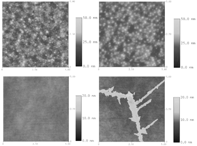 | ||
| Fig. 3 The AFM images of the ED film on ITO and spin-coating film before and after heating at 180 °C and 80 °C for 2 hours, respectively. TBAPF6 was used as supporting electrolyte. Scan rate: 400 mV/s. Scan cycles: 80. Scan range: −0.5 V – 0.85 V. | ||
ED films with a thickness of ∼100 nm can be obtained by multi-cycle CV scans, i.e. 52 scan cycles at a scan rate of 200 mV/s, which require a deposition time of about 12 min. Such ED films washed with acetonitrile and dried in a vacuum oven give a clear surface, then the metal cathode Ba/Al is deposited on the films by vacuum evaporation to construct a prototype electroluminescent device (ITO/ED films/Ba/Al) (see ESI). For ED film obtained by using TBABF4 as supporting electrolyte, the achieved maximum luminescence and luminous efficiency are 134 cd/m2 @ 16.5 V and 0.016 cd/A @ 11 V respectively after optimizing electrochemical parameters. For ED film obtained by using TBAPF6 as supporting electrolyte, the device exhibited a blue electroluminescent (EL) spectrum at λmax 427 with CIE coordinates of (0.16, 0.08), and the achieved maximum luminance and luminous efficiency of the ED film devices are 4224 cd/m2 @ 17 V and 0.47 cd/A @ 11.5 V, respectively (see Fig. 4). The external quantum efficiency for this device is 0.72%. Such device performance is significantly better than that of a TCPC spin-coated device (ITO/PEDOT∶PSS/TCPC/Ba/Al), which has maximum luminance and luminous efficiency of 78 cd/m2 @ 7 V and 0.11 cd/A @ 4.5 V, respectively. The improved performance in the ED film device is likely due to the enhanced thermal stability of morphology and carriers (hole) injection because the dimeric carbazole formed in films as a result of electropolymerization helps hole injection and transport. Though the obtained performance of the ED film device is the best for a single layer OLEDs, an enhancement in brightness and efficiency can be prefigured by utilizing multi-layer ED film involving an emitting layer and a carrier injecting layer. Recently, Roitman and Advincula17 showed that ED films as a hole injecting layer can improve the performance of polymer EL devices.
 | ||
| Fig. 4 Electroluminescent spectra of ED film device. Inset is the relationship between luminance, efficiency and voltage of this device. The ED film used in this device is prepared using deposition parameters: scan range from −0.2 V to 0.85 V, 52 scan cycles at scan rate of 200 mV/s, a mixture of acetonitrile and CH2Cl2 (v/v = 3/2) as solvent, TCPC content of 1 mg/mL and TBAPF6 as supporting electrolyte. | ||
The ED films can be addressed at a well-defined electrode (micrometer size). It provides a new method for fabricating micropatterned polymeric electroluminescent devices, which may have the advantage of simplicity compared with current techniques such as ink-jet printing for polymer-based LEDs18 and shade masking for small-molecular LEDs.19 We have shown a single-color patterning of ED films on ITO (see photo in Fig. 2(b)). In principle, it can be extended to fabricate the “RGB color pixel” by controlling the potential on the ITO strip with state “on” or “off” and changing the electrolytic cell containing various color ED precursors. Extensive ED precursors with green and red fluorescence or phosphorescence and ED films based new precursors or their blends with blue TCPC are being developed by our group.
In summary, the luminescent network films are prepared by a fast and economical electrochemical process. The films exhibit strong blue luminescence, smooth surface morphology and excellent thermal stability of morphology. The OLEDs prepared using these films as a light emitting layer show better performance than the device fabricated by spin-coating films, which demonstrates that the electrochemical synthesis can give highly luminescent film via reasonable molecular design and controlled electrochemical deposition conditions.
We are grateful for financial support from the National Science Foundation of China (grant numbers 20474024, 20573040, 90501001, 50473001), the Ministry of Science and Technology of China (grant number 2002CB6134003) and PCSIRT.
Notes and references
- P. Sigwalt, G. Wegner, J. Morin, M. Leclerc, D. Adès and A. Siove, Macromol. Rapid Commun., 2005, 26, 761 CrossRef CAS.
- C. Weder, Chem. Commun., 2005, 5378 RSC.
- H. Yu, B. Xu and T. M. Swager, J. Am. Chem. Soc., 2003, 125, 1142 CrossRef CAS.
- Y. Liu and C. Tsai, Chem. Mater., 2003, 15, 320 CrossRef CAS.
- J. L. Reddinger and J. R. Reynolds, Adv. Polym. Sci., 1999, 145, 57 CAS.
- E. J. W. List, R. Guentner, P. Scanducci de Freitas and U. Scherf, Adv. Mater., 2002, 14, 374 CrossRef CAS.
- P. Marrec, C. Dano, N. Gueguen-Simonet and J. Simonet, Synth. Met., 1997, 89, 171 CrossRef CAS.
- P. Damlin, T. Östergård, A. Ivaska and H. Stubb, Synth. Met., 1999, 102, 947 CrossRef CAS.
- T. Östergård, C. Kvarnström, H. Stubb and A. Ivaska, Thin Solid Films, 1997, 311, 58 CrossRef CAS.
- L. M. Goldenberg, V. I. Krinichnyi and I. B. Nazarova, Synth. Met., 1991, 44, 199 CrossRef CAS.
- W. Chang, W. Whang and P. Lin, Polymer, 1996, 37, 1513 CrossRef CAS.
- C. Xia, R. C. Advincula, A. Baba and W. Knoll, Chem. Mater., 2004, 16, 2852 CrossRef CAS.
- M. Saçak, U. Akbulut, C. Cheng and D. N. Batchelder, Polymer, 1994, 35, 2495 CrossRef CAS.
- S. A. Saraç, E. Sezer and B. Ustamehmetoglu, Polym. Adv. Technol., 1997, 8, 556 CrossRef.
- Z. H. Wei, J. K. Xu, G. M. Nie, Y. K. Du and S. Z. Pu, J. Electroanal. Chem., 2006, 589, 112 CrossRef CAS.
- F. Tran-Van and C. Chevrot, Electrochim. Acta, 2002, 47, 2927 CrossRef CAS.
- S. Inaoka, D. B. Roitman and R. C. Advincula, Chem. Mater., 2005, 17, 6781 CrossRef CAS.
- B. J. de Gans, P. C. Duineveld and U. S. Schubert, Adv. Mater., 2004, 16, 203 CrossRef CAS.
- Z. Shen, P. E. Burrows, V. Bulovic, S. R. Forrest and M. E. Thompson, Science, 1997, 276, 2009 CrossRef CAS.
Footnote |
| † Electronic supplementary information (ESI) available: Material structure determination, electrochemistry, FT-IR spectra, SEM, AFM and OLEDs fabrication. See DOI: 10.1039/b607242a |
| This journal is © The Royal Society of Chemistry 2006 |