An electrochemical/photochemical information processing system using a monolayer-functionalized electrode†
Ronan
Baron
a,
Avital
Onopriyenko
a,
Eugenii
Katz
a,
Oleg
Lioubashevski
a,
Itamar
Willner
*a,
Sheng
Wang
b and
He
Tian
b
aInstitute of Chemistry, The Hebrew University of Jerusalem, Jerusalem, 91904, Israel. E-mail: willnea@vms.huji.ac.il; Fax: 972-2-6527715; Tel: 972-2-6585272
bLaboratory for Advanced Materials, Institute of Fine Chemicals, East China University of Science and Technology, Shanghai, 200237, P. R. China. E-mail: tianhe@ecust.edu.cn; Fax: 86 21 64252288; Tel: 86 21 64252756
First published on 23rd February 2006
Abstract
An electroactive and photoisomerizable monolayer associated with a Au electrode acts as a Write–Read–Erase information processing system and as a flip-flop Set/Reset memory element.
Photoisomerizable molecular assemblies have been extensively studied in the past two decades as information storage systems.1 For example, spiropyranes,2 azobenzene,3 fulgides,3 and bis-thiophene ethylene4 derivatives were examined as photoactive materials for information processing. Alternatively, the electrochemical storage of information by electroswitchable molecular structures5,6 and the magnetic storage of information using transition metal complexes7 were reported. The readout and erasure of the encoded information is of particular interest to develop ‘Write–Read–Erase’ systems. The electrochemical transduction of photonically-encoded information was accomplished in solution8 as well as on surfaces,9 and electrochemically encoded information could be read out by transient electrochemical means10 or in the presence of hydrophobic magnetic nanoparticles.11 Here we wish to report on a coupled electrochemical/photochemical system using a bis-bipyridinium-bis-thiophene-ethylene derivative as the active material for information encoding and processing. We discuss the functions of the system as a flip-flop Set/Reset memory element, or as a ‘Write–Read–Erase’ information processing unit, and describe the amplification of the readout signals by means of an electrocatalytic process.
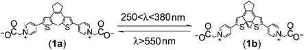
1,2-Bis[2-methyl-5-(4-pyridyl)-3-thienyl]cyclopentene12 was reacted with bromoacetic acid to yield the water-soluble 1,2-bis[2-methyl-5-(4-pyridinium)-3-thienyl]cyclopentene-N,N′-bisacetic acid (1a). A gold electrode was modified with cysteamine hydrochloride and (1a) was covalently linked to the functionalized electrode to yield a monolayer of (2a) (Scheme 1). Fig. 1 shows the cyclic voltammogram of the modified electrode. Two quasi-reversible oxidation waves are observed at +0.1 V and +0.5 V (vs. SCE), respectively. Coulometric assay of the first or the second anodic peak indicates a surface coverage of (2a) that corresponds to 8 × 10⁻¹¹ mole cm−2. This value is very similar to the coverage assayed by microgravimetric quartz-crystal microbalance, QCM, analysis, 7 × 10⁻¹¹ mole cm−2. Fig. 2(A), curve (a), shows the cyclic voltammogram of the (2a)-functionalized electrode in the potential range of −0.1 V to +0.35 V. The quasi-reversible wave for the formation of the radical cation derived from (2a) is observed. The electron transfer rate constant was estimated to be 0.13 s−1 from the peak to peak separation according to Laviron theory.13 Keeping a potential that corresponds to +0.35 V for a time-interval of 90 seconds on the electrode, results in the cyclic voltammogram depicted in Fig. 2(A), curve (b). The peaks are almost depleted. Irradiation of the electrode with filtered visible light, 570 nm, for a time-interval of 15 minutes restores the peaks of the (2a)-functionalized electrode, that reveals cyclic electrochemical/photochemical properties, Fig. 2(A), curve (c). That is, electrochemical biasing of the electrode at +0.35 V results in an interface that lacks electrochemical functions, but irradiation of the interface with visible light restores the (2a)-functionalized surface, Fig. 2(B).
 | ||
| Scheme 1 Assembly of (2a) on the electrode surface, electrochemical ring-closing into (2b) and photochemical ring-opening into (2a). | ||
 | ||
| Fig. 1 Cyclic voltammogram of (2a) immobilized on a Au electrode surface, 0.7 cm2, under Ar, in phosphate buffer, 0.1 M, pH = 7.2, at 100 mV s−1. | ||
 | ||
| Fig. 2 (A) Cyclic voltammogram of the (2a)/(2b)-modified Au electrode, 0.7 cm2, in phosphate buffer, pH = 7.2 at 100 mV s−1; a) the (2a) monolayer-functionalized electrode, b) after application of a potential of +0.35 V for 90 s, c) after irradiation at 570 nm for 15 min. (B) Peak current values obtained upon repetition of the steps described in (A). (C) Optical absorbance of the compounds (1a)/(1b) in solution, a) after electrolysis for 90 min at 0.35 V, b) after irradiation for 90 min at 570 nm. | ||
To account for the electrochemical/photochemical switchable functions of the monolayer interface, we have studied the quantitative electrolysis of (1a) in solution, while following the absorbance features of the electrogenerated product and the subsequently photogenerated species. The electrolysis of (1a) in phosphate buffer solution, pH = 7.2, for 90 min, yielded the absorption spectrum shown in Fig. 2(C), curve (a). Irradiation of the electrogenerated compound for 90 min, λ = 570 nm, yields the spectrum shown in Fig. 2(C), curve (b). The absorbance band at 670 nm decreases in intensity, while the absorbance at 400 nm is intensified. Similar spectral changes were observed upon the well established photochemical isomerization of 1,2-bis[2-methyl-5-(4-pyridyl)-3-thienyl]cyclopentene. The irradiation of (1a) in an aqueous solution with 250–380 nm filtered light yields the closed isomer (1b) that exhibits an identical spectrum to that formed upon the electrochemical oxidation of (1a). Irradiation of (1b) with visible light λ > 550 nm restores the open isomer (1a) and its characteristic absorption spectrum, eqn (1).
 | (1) |
Thus, the (2a)-functionalized electrode undergoes an electrochemically-induced electrocyclic isomerization to form the (2b)-modified surface. The electrocyclized product undergoes photochemical ring-opening to (2a). It should be noted that the electrocyclized product (2b) does not reveal any redox-response in the potential range of 0 V to 0.7 V. Although the mechanism for the electrocyclization of (2a) is not fully understood, it is clear that the electrocyclized radical-cation is derived from (2a). The resulting radical-cation may then undergo cyclization and disproportionation, to yield (2b). In fact, electro-stimulated isomerization of bis-thiophene radical-cation was reported.14
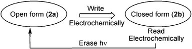
The analysis of the electrochemical/photochemical properties of the monolayer-functionalized electrode reveals a unique system, where electronic or optical signals may lead to Write–Read–Erase functions: the open form (2a) can act as an information recording interface. The information is encoded electrochemically by producing (2b) (Scheme 2). The encoded information is then read out electrochemically (fast scan) and the stored information is erased by a photochemical step that transforms (2b) to (2a).
 | ||
| Scheme 2 ‘Write–Read–Erase’ photo-electrochemical system based on the electrocyclization of (2a) and opening of (2b). | ||
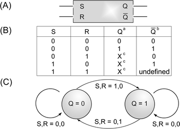
While logic gates provide an output response signal as a result of an input, they do not store the information. Sequential logic operation allows the construction of memory elements. The flip-flop memory elements represent a series of two-state devices that offer memory for sequential logic operations. Among the different flip-flop units the ‘Set/Reset’ is an important memory element, Scheme 3 (A).15 In this memory unit, a logic input Set (S) of ‘1’ and Reset (R) input ‘0’ yields an output of ‘1’ if the memory state is initially either ‘1’ or ‘0’. Similarly, the flip-flop resets to ‘0’ if the input Set is ‘0’ and the Reset input is ‘1’ when the device state is initially either ‘0’ or ‘1’. Set and Reset inputs of ‘0’ do not change the system state, while Set and Reset values of ‘1’ yield an undefined state to define. The truth table for the Set/Reset element is given in Scheme 3(B), and a state diagram for the operation of the Set/Reset flip-flop element is depicted in Scheme 3(C). The photochemical/electrochemical transformations between (2a) and (2b) associated with the electrode also follow the operations of a Set/Reset flip-flop memory unit. The irradiation of the system with a wavelength, λ = 570 nm, corresponds to a Set input ‘1’, whereas the application of a potential of E = 0.35 V on the functionalized electrode corresponds to a Reset input ‘1’. The ‘open’, electrochemically active configuration of the monolayer, (2a), will be considered as the high output memory state of the element, logic ‘1’, while the ‘closed’ photoactive (but electrochemically inactive) monolayer configuration, (2b), will be defined as the logic state ‘0’ of the element. The precise state of the element before or after the application of the respective inputs is read out by applying a rapid cyclic voltammetry scan and examining the electrical response of the system. The operation of the system as a flip-flop Set/Reset memory element is then easily realized; when the system is in the logic state ‘1’, (2a), or when the logic state of the system is ‘0’, (2b), and it is subjected to the S, R inputs (1,0) the system is set to logic state ‘1’. When the system exists in the logic state ‘1’, (2a), or when the system is in the ‘0’, (2b), state and the S, R inputs (0,1) are applied on the system, the reset of the system to state ‘0’, (2b), is accomplished. Obviously, the application of the S, R (0,0) inputs on either state ‘1’ or ‘0’ does not change the system state, while the use of the inputs (1,1) yields a system with an unidentified state since the two inputs contradict one another.
 | ||
| Scheme 3 (A) The flip-flop Set/Reset memory element. (B) Truth table for operations of the Set/Reset, a) element state before and b) after the application of the inputs, c) X means that the output Q will have the same value if Q is either ‘1’ or ‘0’. (C) Graphic representation of the Set/Reset flip-flop device. | ||
The amplification of electrical signals transducing the information storage process is a challenging topic in this field. This is accomplished by the coupling of the electroactive compounds that transduce the storage process to a secondary electrocatalytic16 or biocatalytic process.17 We find that the electrogenerated radical cation formed upon the oxidation of the (2a)-monolayer-functionalized electrode catalyses the oxidation of 1,4-dihydronicotinamide adenine dinucleotide, NADH. Fig. 3(A) shows the cyclic voltammograms of the (2a)-modified-electrode in the presence of different concentrations of NADH. An electrocatalytic anodic current at the potential corresponding to the oxidation of the (2a)-monolayer of the respective radical cation is observed. The derived calibration curve is depicted in Fig. 3(B). Biasing the (2a)-monolayer-modified electrode at +0.35 V for 90 seconds results in the (2b)-functionalized electrode that is inactive towards the electrocatalytic oxidation of NADH. By the photochemical isomerization of the (2b) monolayer to the (2a) state the electro-oxidation of NADH is re-activated. Fig. 3(C) shows the cyclic switchable photochemical/electrochemical activation and deactivation of the electrocatalyzed oxidation of NADH, respectively.
 | ||
| Fig. 3 (A) Cyclic voltammograms of (2a)-modified Au electrode, 0.7 cm2, in phosphate buffer, pH = 7.2 at 20 mV s−1, upon addition of a) 0 mM, b) 1 mM, c) 2 mM and d) 3 mM NADH. (B) Corresponding calibration curve at the potential of 0.27 V. (C) Repetitive measurements of the catalytic current obtained at 100 mV s−1, in the presence of NADH, 5 mM, a) after irradiation at 570 nm for 15 min, b) after application of a potential of +0.35 V for 90 s. | ||
In conclusion, the present study has demonstrated the assembly of a monolayer-functionalized electrode that allows the sequential electrochemical and photochemical storage of information.
This research is supported by the Israel-China Bi-national Program, The Israel Ministry of Science. H. T. acknowledges support by NSFC/China (90401026 and 20476027).
Notes and references
- B. L. Feringa, Molecular Switches, Wiley-VCH, Weinheim, Germany, 2001 Search PubMed; A. N. Shipway and I. Willner, Acc. Chem. Res., 2001, 34, 421 Search PubMed; A. P. de Silva and N. D. McClenaghan, Chem.–Eur. J., 2004, 10, 574 CrossRef CAS.
- I. Willner, R. Blonder and A. Dagan, J. Am. Chem. Soc., 1994, 116, 3121 CrossRef CAS.
- S. Kobatake and M. Irie, Annu. Rep. Prog. Chem., Sect. C: Phys. Chem., 2003, 99, 277 RSC.
- K. Matsuda and M. Irie, J. Photochem. Photobiol., C, 2004, 5, 169 CrossRef CAS.
- C. P. Collier, G. Mattersteig, E. W. Wong, Y. Luo, K. Beverly, J. Sampaio, F. M. Raymo, J. F. Stoddart and J. R. Heath, Science, 2000, 289, 1172 CrossRef CAS.
- E. Katz, O. Lioubashevsky and I. Willner, J. Am. Chem. Soc., 2004, 126, 15520 CAS.
- O. Sato, T. Iyoda, A. Fujishima and K. Hashimoto, Science, 1996, 272, 704 CrossRef CAS.
- S. L. Gilat, S. H. Kawai and J.-M. Lehn, Chem.–Eur. J., 1995, 1, 275 CrossRef CAS; S. H. Kashai, S. L. Gilat, R. Ponsinet and J.-M. Lehn, Chem.–Eur. J., 1995, 1, 285 CrossRef CAS.
- Z. F. Liu, K. Hashimoto and A. Fujishima, Nature, 1990, 347, 658 CrossRef CAS; A. Doron, E. Katz, M. Portnoy and I. Willner, Angew. Chem., Int. Ed. Engl., 1996, 35, 1535 CrossRef CAS.
- I. Willner, V. Pardo-Yissar, E. Katz and K. T. Ranjit, J. Electroanal. Chem., 2001, 497, 172 CrossRef CAS.
- E. Katz and I. Willner, Chem. Commun., 2005, 5641 RSC.
- B. Qin, R. Yao, X. Zhao and H. Tian, Org. Biomol. Chem., 2003, 1, 2187 RSC.
- E. Laviron, J. Electroanal. Chem., 1979, 101, 19 CrossRef CAS.
- Y. Moriyama, K. Matsuda, N. Tanifuji, S. Irie and M. Irie, Org. Lett., 2005, 7, 3315 CrossRef CAS.
- R. J. Tocci, Digital Systems, Prentice-Hall, Ingelwood Cliffs, NJ, 5th edn., 1991 Search PubMed.
- A. Doron, M. Portnoy, M. Lion-Dagan, E. Katz and I. Willner, J. Am. Chem. Soc., 1996, 118, 8937 CrossRef CAS.
- I. Willner, A. Doron, E. Katz, S. Levi and A. J. Frank, Langmuir, 1996, 12, 946 CrossRef CAS; M. Lion-Dagan, E. Katz and I. Willner, J. Chem. Soc., Chem. Commun., 1994, 2741 RSC.
Footnote |
| † Electronic supplementary information (ESI) available: preparation of compound (1a), electrode modification procedure and experimental conditions for electrochemical and light irradiation experiments. See DOI: 10.1039/b518378b |
| This journal is © The Royal Society of Chemistry 2006 |