Zirconium and hafnium oxoclusters as molecular building blocks for highly dispersed ZrO2 or HfO2 nanoparticles in silica thin films
Lidia
Armelao
a,
Christoph
Eisenmenger-Sittner
b,
Matthijs
Groenewolt
c,
Silvia
Gross
*a,
Cinzia
Sada
d,
Ulrich
Schubert
e,
Eugenio
Tondello
a and
Andrea
Zattin
a
aCNR–ISTM and INSTM, Department of Chemical Sciences, University of Padova, via Marzolo, 1- I-35131, Padova, Italy. E-mail: silvia.gross@unipd.it; Fax: ++39-049-8275161; Tel: ++39-049-8275736
bInstitut für Festkörperphysik-Vienna University of Technology, Vienna, Austria
cMax-Planck-Institut für Kolloid- und Grenzflächenforschung, Golm, Germany
dDepartment of Physics, University of Padova, Padova, Italy
eInstitute of Materials Chemistry-Vienna University of Technology, Vienna, Austria
First published on 3rd March 2005
Abstract
A novel synthetic route for the preparation of ZrO2 or HfO2 nanoparticles homogeneously dispersed in SiO2 thin films was developed. This route is based on the copolymerisation of organically modified crystalline oxozirconium or oxohafnium clusters (M4O2(OMc)12, M = Zr, Hf; OMc = OC(O)–C(CH3)![[double bond, length as m-dash]](https://www.rsc.org/images/entities/char_e001.gif) CH2) with (methacryloxymethyl)triethoxysilane (MAMTES, CH2C(CH3)C(O)O–CH2Si(OCH2CH3)3). These crystalline clusters, which are the precursors for the corresponding metal oxides (MO2), were prepared via the sol–gel route by reaction of zirconium or hafnium butoxide (M(OBu)4) with methacrylic acid. The copolymerisation of the clusters with the methacrylate-functionalised siloxane was photoinitaited by Irgacure 184 and allowed the anchoring of the cluster to the forming silica network. The solution was cast into films by dip-coating and UV cured (10 min, 125 W) to promote the copolymerisation of the methacrylate groups of the cluster with those of the silane. Transparent and homogeneous films 200–450 nm thick were obtained after calcination at 800 °C in air. This route allowed the production of a very homogeneous dispersion of the MO2 precursors inside the silica matrix. The surface and in-depth composition of the thin films was investigated through IR, X-ray photoelectron spectroscopy (XPS) and secondary ion mass spectrometry (SIMS). SIMS and XPS depth profiles evidenced a very homogenous distribution of both zirconium or hafnium throughout the silica films and sharp film–substrate interfaces. The surface morphology of the coatings was investigated through atomic force microscopy (AFM), which showed smooth, homogeneous and crack-free surfaces. Through X-ray diffraction (XRD) the crystallisation of hafnium and zirconium oxides was revealed, while the presence of isolated crystalline nanoparticles having a diameter of 5–10 nm was evidenced by transmission electron microscopy (TEM). A pull-off test indicated a very good adhesion of the films to the substrate.
CH2) with (methacryloxymethyl)triethoxysilane (MAMTES, CH2C(CH3)C(O)O–CH2Si(OCH2CH3)3). These crystalline clusters, which are the precursors for the corresponding metal oxides (MO2), were prepared via the sol–gel route by reaction of zirconium or hafnium butoxide (M(OBu)4) with methacrylic acid. The copolymerisation of the clusters with the methacrylate-functionalised siloxane was photoinitaited by Irgacure 184 and allowed the anchoring of the cluster to the forming silica network. The solution was cast into films by dip-coating and UV cured (10 min, 125 W) to promote the copolymerisation of the methacrylate groups of the cluster with those of the silane. Transparent and homogeneous films 200–450 nm thick were obtained after calcination at 800 °C in air. This route allowed the production of a very homogeneous dispersion of the MO2 precursors inside the silica matrix. The surface and in-depth composition of the thin films was investigated through IR, X-ray photoelectron spectroscopy (XPS) and secondary ion mass spectrometry (SIMS). SIMS and XPS depth profiles evidenced a very homogenous distribution of both zirconium or hafnium throughout the silica films and sharp film–substrate interfaces. The surface morphology of the coatings was investigated through atomic force microscopy (AFM), which showed smooth, homogeneous and crack-free surfaces. Through X-ray diffraction (XRD) the crystallisation of hafnium and zirconium oxides was revealed, while the presence of isolated crystalline nanoparticles having a diameter of 5–10 nm was evidenced by transmission electron microscopy (TEM). A pull-off test indicated a very good adhesion of the films to the substrate.
1. Introduction
The need for advanced materials endowed with enhanced properties has progressively focused on composite systems which can involve complex stoichiometries or architectures. In this area, the development of synthetic strategies which enable a precise control over the evolution of the precursor to give the final solid-state system has become a major concern in many technological and scientific fields. Noticeable attention has been focused on mixed oxide materials and on their preparation via the sol–gel process.1,2However, for the preparation of multicomponent oxide systems, a major disadvantage is represented by the different hydrolysis and condensation rates of the precursors, which can lead to heterogeneous mixtures. To circumvent this drawback and to obtain multicomponent materials homogeneous at a molecular level, different strategies have been devised, among which the design of suitable precursors represents a key concern. Different hybrid materials containing both silica and other metal oxides have been formerly prepared by mixing metal alkoxides (e.g. Zr, Ti) with methacrylic acid as complexing ligands bearing the polymerisable moiety, and methacryloxysilanes.3–5 Inorganic–organic hybrid materials in which metal oxide precursors are homogenously embedded into a silica matrix can be conveniently used as “composite precursors” for the preparation of binary oxide systems of the type MOx:SiO2 in which the metal oxide is evenly dispersed in the silica matrix. The thermal calcination of the starting hybrid materials at high temperature (>600 °C) promotes the pyrolysis of the organic parts and the densification of the oxide networks, thus enabling the preparation of pure and homogeneous composite oxide materials, either as bulk or thin films.
Among these oxides, increasing attention has been devoted to zirconium and hafnium oxides. In particular, mixed zirconia–silica and hafnia–silica materials are potentially useful in a wide spectrum of technological applications, for instance in catalysis,6,7 as catalyst supports8 or in optics.3 It has been reported that Zr/Si binary oxides prepared by the sol–gel route show catalytic activity for the selective formation of isobutene.9 Sol–gel ZrO2–SiO2 materials have been catalytically tested for isopropanol and n-butanol dehydration.10 Zr/Si binary oxides having strong acid sites have been also found to exhibit catalytic activity for the dehydrogenation of cyclohexanol.11 These mixed oxides display enhanced physico-chemical properties such as high thermal and chemical stability. Zirconia–silica glasses have also been carefully investigated as structural materials, thanks to their low thermal expansion, high fracture toughness and excellent resistance to chemicals.12,13 Furthermore, binary zirconia–silica and hafnia–silica in the form of thin films are appealing replacements for silicon dioxide as gate dielectric materials for complementary metal-oxide-semiconductor (CMOS) transistors.14–16 Zirconia and hafnia are known to be thermodynamically stable when in contact with silicon.14–16 These binary oxide “alloys” are expected to provide enhanced permittivity with respect to SiO2, while the silica component should impart crystallisation resistance and an electrically neutral interface.17
As already mentioned, the properties of these binary systems are strongly affected by the composition, the microstructure and the degree of mixing of the two oxide components. Consequently, the choice of a suitable synthetic route enabling control of the mentioned features would enable a fine tailoring of the final properties. These binary systems have been recently prepared by chemical solution deposition,18 ultrahigh vacuum molecular beam epitaxy19 and conventional sol–gel processing starting from the corresponding alkoxides.2,20,21
In this study, we propose the implementation of a method based on the use of methacrylate-substituted transition metal oxoclusters M4O2(OMc)12 (M = Zr, Hf) and of a methacryloxysilane for the preparation of silica thin films with embedded hafnia or zirconia. The clusters, which are precursors for the corresponding oxides, are easily prepared by reaction of metal alkoxides with methacrylic acid, as reported elsewhere.22–24 The methacrylate moieties of the cluster and that of the silane are copolymerised, while the alkoxy groups of the silane undergo hydrolysis and condensation reactions to form a silica network. These and similar metal oxoclusters have been already used as inorganic building blocks for the synthesis of a wide variety of inorganic–organic hybrid materials.24–27 The advantage of the approach reported in this article, compared to the processing of mixtures of metal alkoxides, methacrylic acid and methacrylate-substituted silanes (see above) is that the use of the pre-formed clusters allows better structural control on the composite materials obtained. Although the final materials are mixed-metal oxides, our approach allows the use of polymer processing methods, which are particularly useful for the preparation of composite films.
In the present study, the composition, the morphology, and the microstructure of xZrO2–(100![[thin space (1/6-em)]](https://www.rsc.org/images/entities/char_2009.gif) −x)SiO2 and xHfO2–(100−x)SiO2
(x
= molar, 0 < x < 17) thin films were investigated. In particular, the in-depth distribution of the host zirconium and hafnium oxides in the silica matrix was analysed by performing XPS and SIMS depth profiles.
−x)SiO2 and xHfO2–(100−x)SiO2
(x
= molar, 0 < x < 17) thin films were investigated. In particular, the in-depth distribution of the host zirconium and hafnium oxides in the silica matrix was analysed by performing XPS and SIMS depth profiles.
2. Experimental
Chemicals
(Methacryloxymethyl)triethoxysilane (purchased from Gelest); methacrylic acid 99%, anhydrous tetrahydrofuran and anhydrous toluene, purchased from Aldrich, were used as received. The photoinitiator Irgacure 184 (I184) was purchased from CIBA Specialty Chemicals Inc. All the chemicals were stored under argon. The clusters M4O2(OMc)12 (M = Zr, Hf) were synthesised by the previously reported procedure.22,23Precursor solutions
All operations were performed under argon using standard Schlenk techniques. The preparation of the starting solution used for the film deposition can be described as a three step process, which is schematically sketched in the flow chart in Fig. 1.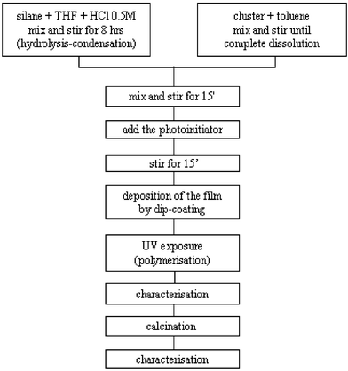 | ||
| Fig. 1 Flow-chart showing the synthesis route. | ||
First, (methacryloxymethyl)triethoxysilane (MAMTES) was dissolved in THF and prehydrolysed with water in the presence of HCl as catalyst for 8 h at room temperature. The typical composition of the sol–gel solution is silane–H2O–HCl 1 : 4 : 0.04 molar ratio. The hydrolysis time was chosen on the basis of time-resolved infra-red studies of the hydrolysis rate of the silane, as reported elsewhere.28 A calculated amount of the crystalline cluster was dissolved in toluene and this solution was then mixed with the prehydrolysed silane and stirred at room temperature for 15 min. To this solution, the radical photoinitiator CIBA Irgacure 184 (1-hydroxycyclohexyl-1-phenylketone) was added (1% w/w with respect to silane) with stirring. When excited to its triplet state by UV radiation, the molecule undergoes α-cleavage to produce benzoyl and 1-hydroxycyclohexyl radicals. The former is primarily responsible for initiating the polymerisation of the methacryloxypropyl group. Different samples were prepared by varying a) the type of cluster (Hf or Zr) and b) the silane : cluster molar ratio. As a reference, the MAMTES silane without addition of hafnium or zirconium clusters was also cast into film and UV cured. Table 1 summarises the different molar ratios used for the preparation of the samples, according to the nominal composition of the solution. In Table 1 and subsequently, the labels “SiZr” and “SiHf” indicate the specimens prepared by using the zirconium and hafnium oxoclusters, respectively, while the number indicates the Si/M (M = Zr, Hf) atomic ratio.
| Sample | Si/M |
|---|---|
| SiHf5 | 5 |
| SiHf11 | 11 |
| SiHf24 | 24 |
| SiHf39 | 39 |
| SiHf0 | without cluster |
| SiZr5 | 5 |
| SiZr17 | 17 |
| SiZr21 | 21 |
Film deposition and UV curing
The prepared solutions were cast into films by a dip-coating procedure. Four different materials were used as substrates: silicon wafers (Si 110), Herasil silica slides, supplied by Hereaus, K-glass slides, supplied by EKOPLUS, consisting of soda–lime–silica on one side, coated with a thin film (<500 nm thick) of fluorine-doped tin oxide (supplied by Isoclima, Este, PD, Italy) and stainless steel plates. Before use, the slides were cleaned and rinsed both in doubly distilled water and 2-propanol. This procedure was repeated several times to remove organic residuals at the surface, thus favouring the best adhesion between coating and substrate. The slides were finally dried in air at room temperature.29Dip-coating film deposition was carried out in air at a constant withdrawal speed of 10 cm min−1, at room temperature with a relative humidity of 30–40% by using home-made equipment. After dip-coating, the films were irradiated under a UV source for 10 min to promote the polymerisation of methacrylate. The irradiation source was a Helios Italquartz s.r.l. lamp with a power of 125 W and an emission range of 250–450 nm. The films were then calcined in air at 800 °C for 3 h to remove the organic groups and to yield the final mixed oxides. Homogeneous and well-adhering films were obtained on all the substrates. Some selected samples were also calcined at 1000 °C for 5 h to investigate their crystallisation behaviour. Transparent and homogeneous films were obtained, having a thickness of 200–450 nm. For some selected samples, the thickness was determined by measuring the crater depth made after the SIMS analysis by a Tencor Alpha Step Profilometer. The values determined for some selected samples are reported in Table 2.
| Sample | Thickness FWHM as prepared/nm | Thickness FWHM after calcination/nm |
|---|---|---|
| SiHf39 | 247 ± 27 | |
| SiHf5 | 198 ± 21 | |
| SiZr17 | 209 ± 18 | |
| SiZr5 | 431 ± 37 | 258 ± 18 |
Thin film characterisation
Transmission FT-IR spectra were recorded with a Nexus 870 FT-IR spectrometer (Nicolet) in the range from 400 to 4000 cm−1, with a resolution of 4 cm−1. The films for the analysis were spun onto a one side of a polished Si wafer.The composition of the films at the surface and in the bulk was investigated by XPS. Photoelectron spectra were run on a Perkin–Elmer Φ 5600ci spectrometer using non-monochromatised Al-Kα radiation (1486.6 eV). The working pressure was <5 × 10⁻⁸ Pa. The spectrometer was calibrated by assuming the binding energy (BE) of the Au4f7/2 line at 83.9 eV with respect to the Fermi level. The standard deviation for the BE values was 0.15 eV. The reported BEs were corrected for the charging effects, assigning the BE value of 285.0 eV to the C1s line of adventitious carbon.30 In the calcined samples, in which no carbon could be detected, charging effects were corrected by assuming that the Si2p peak has the BE typical of silicon in silica, i.e. 103.6 eV. This implies that silicon experiences an environment consisting mostly of oxygen. Considering that, even in the most concentrated sample, the amount of silica is at least 83% at., this assumption can be considered reliable in a first approximation. Survey scans were obtained in the 0–1350 eV range. Detailed scans were recorded for the O1s, Si2p, Zr3d, C1s regions in the case of zirconia–silica films and O1s, Si2p, Hf4f, Hf4d, C1s in the case of hafnia–silica films. The atomic composition was evaluated using sensitivity factors supplied by Perkin–Elmer.31 Depth profiles were carried out by Ar+ sputtering at 3 keV with an argon partial pressure of 5 × 10⁻⁶ Pa. A specimen area of 2 × 2 mm2 was sputtered. A flood gun was used to compensate charging effects on the surface of the irradiated specimens. Samples were introduced directly, by a fast entry lock system, into the XPS analytical chamber.
Glancing incidence XRD patterns were recorded by means of a Bruker D8 Advance diffractometer equipped with a Göbel mirror and a Cu-Kα source (40 kV, 40 mA), at a fixed incidence angle of 1.5°. The average crystallite dimension was estimated from the most intense diffraction peaks by means of the Scherrer equation.
SIMS measurements were carried on a IMS 4f mass spectrometer (Cameca, Padova, Italy) using a 10 kV Cs+ primary beam and by negative secondary ion detection (the sample potential was fixed at −4.5 kV) with a final impact energy of 14.5 keV. The SIMS spectra were carried out under ultra-high vacuum at different primary beam intensities (in the range 30–50 nA) rastering over a nominal 125 × 125 µm2 area. A beam blanking mode was used to improve the depth resolution, interrupting the sputtering process during magnet stabilisation periods. The measurements were performed in high mass resolution configuration to avoid mass interference artefacts. The charge build-up occurring in insulating samples during the in-depth profiling was compensated by an electron gun without any need to cover the surface with a metal film. The erosion speed was evaluated by measuring the depth of the erosion crater at the end of each analysis by means of a Tencor Alpha Step profilometer with a maximum uncertainty of few nanometers. The dependence of the erosion speed on the matrix composition was taken into account for each sample by recording various spectra at different depths in each sample.
AFM images were taken using a Park Autoprobe CP instrument operating in contact mode in air. The micrographs were recorded in 3–4 different areas of each sample, in order to test the film homogeneity. The background was subtracted from the images using the ProScan 1.3 software from Park Scientific.
Transmission electron microscopy (TEM) images were taken with a Zeiss EM 912 at an acceleration voltage of 120 kV. Samples were scraped off from the substrate with a razor blade and brought onto a 400 mesh carbon-coated copper grid. Different areas were investigated in order to check the homogeneity of the material.
3. Results and discussion
Before carrying out the deposition of the films, the UV photoinduced polymerisation process was first monitored by FT-IR to optimise the irradiation time. As the polymerisation process proceeds, the intensity of the acrylate ν(CC) bands at about 1638 cm−1 decreases due to the CC double bond consumption, while the integrated area of the ν(CO) bands remains constant. Consequently, the ν(CC)/ν(CO) area ratio was used as a measure of the degree of conversion. The conversion of the methacrylate moiety was followed by plotting the relative intensity of the double bond vibration versus the irradiation time (Fig. 2).
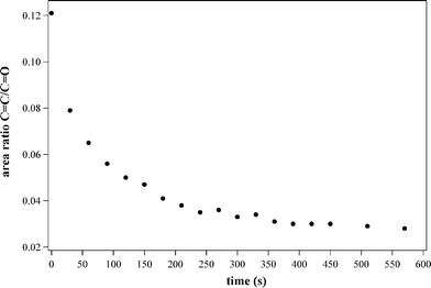 | ||
| Fig. 2 CC/CO intensity ratio as a function of the polymerisation time. | ||
The degree of conversion shows a trend already observed in similar experiments.4 While in the early stage of UV irradiation, the CC bonds are rapidly consumed, a lowering in the reaction rate is observed after about 60 s, since the propagation step requires the diffusion of the monomeric species, which are not highly mobile in the reaction mixture. Although the methacrylate moieties are covalently anchored to an inorganic network already partially crosslinked, a conversion degree of about 70% is reached within about 7 min. After this time, no further decrease of the ν(CC)/ν(CO) ratio is observed and the curve flattens, thus indicating that the polymerisation does not proceed any further. On account of these findings, the deposited films were irradiated for 10 min.
The prepared samples were characterised both as-prepared and after the thermal treatment, to investigate the effect of the temperature on their compositional, microstructural and morphological features. The composition of the thin films containing both zirconium and hafnium clusters was at first investigated through FT-IR spectroscopy. In the following discussion, the spectra of the two systems are considered jointly, since no remarkable difference was observed on going from hafnia- to zirconia-based binary oxides. In Fig. 3 the IR spectra of the sample SiZr21 before (Fig. 3a), and after calcination (Fig. 3b) are compared.
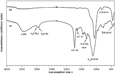 | ||
| Fig. 3 IR spectra of the (a) as-prepared and (b) calcined SiHf11 sample. | ||
The peaks have been assigned according to the values reported in the literature,18,32,33 and the main vibrations are summarised in Fig. 3a and b.
As can be seen in the spectrum reported in Fig. 3a, the typical vibrations of silica are present even in the uncalcined samples. In particular, the typical band of silica at 800 cm−1 was detected, which is ascribed to the symmetric stretching of oxygen in the Si–O–Si group.34 This band is in the same region in which the Si–O–Zr vibration would be expected, and whose wavenumbers, according to literature data, should be found at about 802 cm−1.35 Concerning the as-prepared samples, the intense band at 1118 cm−1 is also evident, which is ascribed to the νas(Si–O–Si) asymmetric stretching of the siloxane group. This band shows a shoulder at 1174 cm−1, whose origin has not yet been clarified. In the literature, shoulders at about 1200 cm−1 have been ascribed to asymmetric stretching in tetranuclear siloxane rings.36 The band ascribed to Si–O–Si is shifted upon calcination and consequent densification to a lower wavenumber, 1069 cm−1, a value close to that reported in the literature, 1080 cm−1. In addition, a further band at 450 cm−1 was also detected, which was ascribed to the rocking vibrations of the Si–O–Si group.34 The peaks at 2960 and 2930 cm−1 are ascribed to the asymmetric stretching νas(CH3) of the not yet completely hydrolysed Si–O–Et groups and to the symmetric νs(CH) stretching of the terminal methylene double bonds respectively.
In the as-prepared samples, the vibrations typical of the organic components of the matrix are also evident. In particular, the sharp band of the CO carbonyl group at 1722 cm−1 and that of the C–O ester group of the methacrylate at 1330 cm−1 are also clearly detected. Due to the overlapping of the bands, the ν(CO) vibration of the methacrylate groups of the cluster could not be identified. In addition, at 1635 cm−1 the band assigned to the CC vibration of the methacrylate double bond was apparent. The fact that this band is still present after UV curing can be ascribed to the lack of complete polymerisation of the methacryloxy moieties of the silane. This can in turn be traced back to the hampered mobility of the methacrylate groups, which are covalently linked to the already partially formed silica network. Furthermore, the steric restrictions imposed by the two isostructural clusters, both bearing 12 methacrylate groups, is also expected to play a role in avoiding the complete copolymerisation of the cluster methacrylate groups with the methacryloxysilane, thus explaining the presence of unreacted double bonds.
In the uncalcined sample, a broad band at 3450 cm−1 was detected. Two different contributions could contribute to the origin of this band: the stretching vibration of the OH groups of water adsorbed on the film surface and the vibration of the Si–OH groups formed upon hydrolysis. In fact, this band disappears upon calcination, which induces a further densification of the matrix through condensation of silanol groups to give Si–O–Si. In the calcined samples, only the silica bands at 1063, 804 and 447 cm−1 are present, while the features typical of the organic parts are completely absent.
On account of these findings, the IR spectra allowed us to conclude that:
• the formation of a polysiloxane network is observed even in the hybrid thin film;
• the methacrylate groups are not completely polymerised, due to the steric hindrance and to the limited mobility imposed by the silica matrix;
• heating induces a complete densification of the matrix and the complete disappearance of the organic components;
• the presence of vibrations ascribable to mixed Si–O–M bonds could not be ascertained.
The surface and in-depth composition of the films was investigated by XPS and SIMS. For the sake of clarity, XPS and SIMS data are discussed together, since the two methods provide complementary and mutually integrated information arising from different depth resolution, erosion capability and speed. Also in this case, for some selected films, the analyses were repeated on the as-prepared as well as on the calcined specimens. For comparison, the surface XPS spectrum of the UV polymerised MAMTES (SiHf0) as-prepared sample was also acquired. This latter sample shows, after calcination, the typical features of a silica network. In particular, the Si2p and O1s regions have binding energies of 103.6 and 533.0 eV respectively. These values are in good agreement with those typical of silicon dioxide, 103.6 and 532.5 eV respectively.31 The O/Si atomic ratio in the analysed specimen is higher than the stoichiometric value, i.e. 2. This finding can be ascribed to the presence of hydroxyl groups on the surface of the silica films.
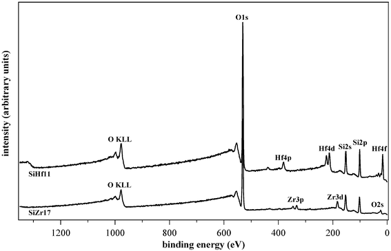
The spectra of as-prepared samples SiZr17, SiHf11 and SiHf0 are shown in Fig. 4, and the spectra of the calcined SiZr17 and SiHf11 samples are shown in Fig. 5.
 | ||
| Fig. 4 Comparision of the as-prepared samples SiHf11, SiZr17 and SiHf0. | ||
 | ||
| Fig. 5 Comparision of the samples SiHf11 and SiZr17 after calcination. | ||
For the elements of interest, detailed scans were also acquired. In the as-prepared samples, all the expected elements (C, Si, O, Zr, Hf) were detected. The composition of the film was analysed on the surface as well as at depth. The samples were sputtered and the analysis of the eroded surface was carried out after each sputtering cycle. By using this operation mode, depth profiles were obtained.
In-depth quantitative analysis performed on both as-prepared and calcined samples reveals an even distribution of the guest zirconium- and hafnium-related species. In Fig. 6, the Si/Zr atomic ratios in the sample SiZr17 before and after the thermal treatment are reported, while in Fig. 7, the Si/Hf atomic ratios in the sample SiHf25 before and after the thermal treatment are plotted.
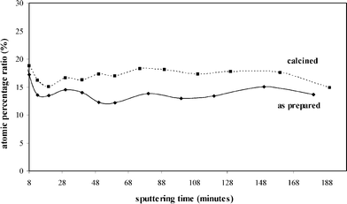 | ||
| Fig. 6 Si/Zr atomic ratio in as-prepared and calcined SiZr17 samples as a function of the sputtering time. | ||
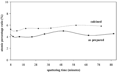 | ||
| Fig. 7 Si/Hf atomic ratio in as-prepared and calcined SiHf11 samples as a function of the sputtering time. | ||
As can be seen in the plots of the ratio of the atomic percentages versus time of sputtering, which can in turn be related to the eroded depth, the guest species are evenly distributed throughout the whole film thickness. It should be pointed out, however, that the lateral distribution of XPS is about 5–10 µm, therefore heterogeneities of a smaller dimension cannot be detected by this technique. This even distribution is observed in both the as-prepared and calcined specimens. These findings confirm that the calcination treatment does not affect the distribution of the species in the samples on the given scale. A significant difference among the two set of samples concerns the carbon content. While in the crude samples, due to the presence of the inorganic–organic hybrid structure, carbon is detected in a considerable amount (40%), a very low content of carbon (<1%) is present after calcination.
Assuming that silicon is mostly present as silica, and by giving Si2p the value of SiO2, i.e. 103.6 eV,31 the binding energy of Zr3d5/2, corrected for charging effects, results in 183.5 eV for sample SiZr17, a value higher than bulk zirconium oxide, i.e. 182.2 eV.31 This finding can be rationalised by considering that in a system consisting of zirconia particles dispersed in a silica matrix, zirconium experiences a chemical environment which is substantially different from that in bulk zirconia. Since Si is more electronegative than zirconium, an Si–O– bond around Zr is expected to withdraw more electron density than a Zr–O environment, which would be expected in the case of a pure zirconium oxide. This in turn implies a shift of the Zr3d BE to higher values, as experimentally observed.
A shift to higher binding energies of the Zr3d peak has already been observed for zirconia–silica binary nanocomposites characterised by a zirconia loading of <20 wt%.37 In particular, in this study, a value of 183.1 eV for a sample containing 9.3 wt% of zirconia was measured, and the shift to higher value was ascribed to the smaller relaxation energy for highly dispersed zirconium oxide species compared to the powdered ZrO2. A similar trend was also observed for the SiHf24 sample, in which the Hf4f is characterised by a BE of 19.3 eV, a value higher than that reported for hafnium oxide, 16.7 eV.31
In the zirconium sample, the atomic percentages obtained by XPS are: 1.7% (Zr), 29.5% (Si), 68.8% (O). These data are in very good agreement with the theoretical ones, i.e. 1.8%, 31.5%, 66.7% for zirconium, silicon and oxygen, respectively. In particular, the experimental Si/Zr atomic ratio is 17, in complete agreement with the calculated ratio (i.e. 17). In the case of the analysed hafnium sample, the measured atomic percentages (3.6% Hf, 66.7% O, 29.4% Si) are also in very good agreement with the nominal composition (2.8% Hf, 66.7% O, 30.5% Si).
The in-depth distribution of zirconium and hafnium in the silica matrix throughout the whole film thickness was further investigated by using SIMS. In particular, SIMS analyses were performed to check the depth profile of the elements and the presence of contaminants in both the as-prepared and calcined samples. Fig. 8a and Fig. 8b report the elemental SIMS profiles of sample SiHf24 before and after thermal treatment, respectively.
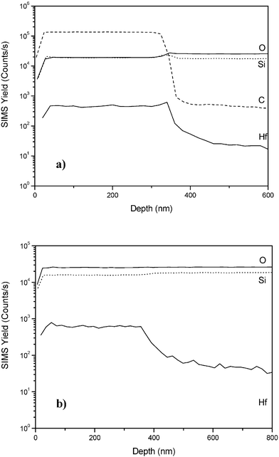 | ||
| Fig. 8 SIMS depth profiles of the sample SiHf24 (a) as-prepared and (b) calcined. | ||
The film thickness in the case of the as-prepared sample was found to be lower than 400 nm and significantly decreased after the calcination treatment due to the densification of the film. The film-to-substrate interface is sharp and the element inter-diffusion layer is lower than 50 nm in the as-prepared sample but increases to 100 nm after calcination. SIMS data also showed that the calcination process does not influence the film composition, since the Hf content appears to remain constant throughout the film, as observed in the as-prepared sample. Similar results were found also in the case of zirconium samples, which are extensively described elsewhere.38
The microstructure of the thin films was investigated through glancing angle X-ray diffraction to minimise the contribution of the silica substrate. The 800 °C calcined samples of both the zirconium- and hafnium-based silica films display a featureless XRD pattern, characterised only by the presence of a broad band peaking at 21.5° and ascribed to amorphous silica. The absence of diffraction peaks can be either ascribed to the presence of amorphous zirconia or hafnia, or to the presence of undetectable crystallites. This latter hypothesis appears more reasonable in our case, since the adopted approach, based on the grafting of the cluster to the forming silica matrix, should favour nucleation and avoid agglomeration of host particles. Selected samples were further calcined twice at 1000 °C for 5 h. After the calcination at 1000 °C, diffraction peaks were observed for both zirconia (Fig. 9a) and hafnia samples (Fig. 9b).
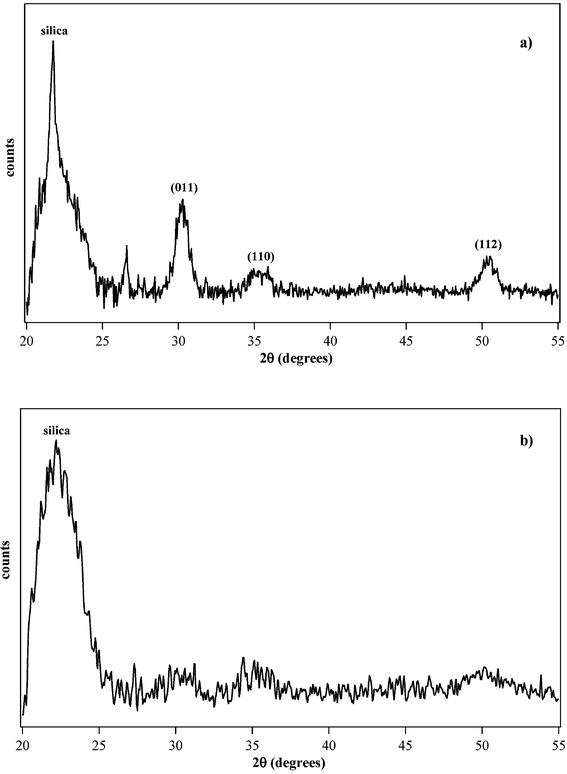 | ||
| Fig. 9 GI-XRD pattern of the samples (a) SiZr5 and (b) SiHf24 calcined at 1000 °C for 5 h. | ||
As far as the SiZr5 zirconia-based sample is concerned, as can be seen in Fig. 9a, sharp peaks were detected which, on the basis of data reported in JCPDS (Joint Commitee on Powder Diffraction Standards), were ascribed to tetragonal zirconia. The most intense peak at 2θ = 22° was ascribed to silica, while the peaks at 30.2° (011), 35.5° (110) and 50.5° (112) were ascribed to tetragonal ZrO2. The second thermal treatment at 1000 °C for 5 h does not remarkably change the diffraction pattern. By applying the Scherrer formula39 to the peak at 30.2°, the zirconia crystallite size was estimated to be 10 nm.
The SiHf24 thin film was calcined as already described for zirconium. In this case, the diffraction pattern, ascribed to the formation of tetragonal hafnia, shows broader peaks than in the case of the zirconia-based sample. The calcination conditions being equal, this fact can be ascribed to a lower content of the guest oxide in the host matrix. While in the case of SiZr5 the zirconium oxide content is about 16.7 mol% with respect to silica, in this latter case the molar amount is 4 mol%.
As already observed in the case of zirconia, a noticeable delay in crystallisation was also observed for the hafnia-based sample.19
The crystallisation of these binary systems has been thoroughly investigated, since, as mentioned, the obtainment of microstructurally homogeneous materials is a key concern to be addressed, and since phase transitions can dramatically affect the properties of the final materials.17,40–48 Generally, the crystallisation of tetragonal zirconia has been reported to occur after calcination at 400 °C,18 while partial transformation from tetragonal to monoclinic was reported to occur at 800–900 °C, and the single monoclinic phase was present at temperatures higher than 1000–1200 °C. In a previous study by Neumayer,18 addition of silica to zirconium and hafnium oxide was found to increase the temperature of crystallisation of zirconium oxide, to stabilise the formation of tetragonal hafnia and to increase the temperature at which the transformation of ZrO2 or HfO2 from the tetragonal to the monoclinic phase occurs. The lower the content of hafnia or zirconia, the higher the crystallisation temperature. As extensively reported by Terry et al.,49 the initial formation of the thermodynamically unstable tetragonal (t) zirconia and the delayed formation of monoclinic (m) zirconia have been explained in terms of surface and strain energies of hafnia or zirconia nanoparticles and in the hindered nucleation of the martensitic t/m transition, which is also slightly displacive. Whenever zirconia or hafnia are homogeneously dispersed in a silica matrix, the crystallisation requires both diffusion as well as grain growth, and a correlation between this delayed crystallisation and the homogeneity of the materials has been established.49 Well-mixed samples display higher crystallisation temperature,50 which in turn make them suitable for high temperature applications thanks to their enhanced resistance to the “thermal shock” associated with the martensitic transformation mentioned.
As described, XPS and SIMS depth profiles show a homogeneous distribution of the host species. A homogeneous depth profile of the species involved (Si, O, Hf/Zr) could be ascribed either to a) a complete intermixing of the host oxide with the guest matrix (formation of a mixed oxide solid solution), or b) to the formation of well-distributed guest clusters in the host matrix smaller than the lateral resolution of the two methods. The TEM micrographs acquired to further investigate the distribution of the clusters into the matrix definitely rule out this former hypothesis and clearly show the presence of isolated clusters. The two calcined samples SiZr5 and SiHf24, characterised by different compositions, were analysed by TEM (Fig. 10 and Fig. 11, respectively).
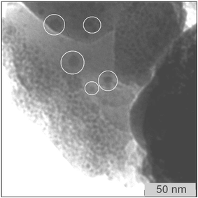 | ||
| Fig. 10 TEM micrograph of the calcined SiZr5 sample. | ||
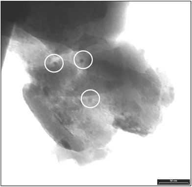 | ||
| Fig. 11 TEM micrograph of the calcined SiHf24 sample. | ||
In both samples isolated nanoparticles having a diameter of 5–10 nm were detected. The average diameter of particles seen in the TEM images correlates well with the crystallite size obtained from the XRD data by the Scherrer equation. The presence of crystalline nanoparticles of hafnia in SiHf24 and zirconia in SiZr5 was proved by electron diffraction (data not shown). The SiZr5 sample, characterised by a quite high concentration of zirconia, shows also some agglomeration, which can be ascribed to the relatively high concentration of zirconia in the silica matrix, leading to some coalescence of the nanoparticles. On the contrary, these agglomeration phenomena are not observed in the more diluted sample containing hafnia clusters.
The morphology of the thin films was analysed by AFM. For each analysed sample, three micrographs of different surface areas were examined to test the topography uniformity of the films. The zirconia- and hafnia-based samples are characterised by a quite smooth, crack-free and homogeneous surface. The surface morphology of the sample SiZr17 before and after calcination is shown in Fig. 12.
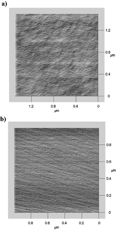 | ||
| Fig. 12 AFM micrographs of the samples SiZr17 (a) as-prepared and (b) calcined. | ||
The average roughness of the specimens was also evaluated; the values obtained for two samples before and after calcination are summarised in Table 3.
| Sample | Thermal treatment | Mean roughness/nm |
|---|---|---|
| SiZr21 | None | 0.5 |
| SiZr17 | 800 °C for 3 h | 0.4 |
| SiHf24 | None | 0.6 |
| SiHf24 | 800 °C for 3 h | 0.4 |
The adhesion of the films on the substrate was evaluated by pull-off tests. Two different series of calcined samples, each consisting of 4 specimens and characterised by two different compositions, namely SiZr0 and SiZr5, were tested. Both series provided an average adhesiveness value of about 650 N cm−2, thus showing that the presence of the cluster does not significantly influence the adhesion. This value can be viewed as a lower bound of the adhesiveness, since in most cases the bonding tape (SCOTCH-WELD™ brand bonding film 588) used to contact the test stud to the coating failed. Direct bonding of the test stud to a glass substrate yielded similar values, so the adhesion of the coating to the substrate can be considered as excellent.
4. Conclusion
ZrO2–SiO2 and HfO2–SiO2 films of different composition were grown by a modified sol–gel procedure, involving the use of a bifunctional siloxane and of Hf- and Zr-oxoclusters as molecular building blocks. The approach adopted has been proved to be effective for obtaining a homogeneous distribution of the two guest oxides in the host silica matrix and to favour the formation of well-dispersed nanosized clusters. In particular, XPS and SIMS depth profiles indicate a very smooth distribution of the two oxides throughout the whole thickness of the layers. From XRD data, the addition of silica to the two oxides was found to increase the crystallisation temperature of the crystalline phase. This has been ascribed to the preservation of the molecular-level homogeneity in the transition from the solution precursors to the final ceramic materials. TEM micrographs confirmed the presence of isolated crystalline clusters of zirconia and hafnia whose size, in agreement with XRD data, is about 5–10 nm.The grafting of the clusters (the molecular precursors for the guest oxides) to the bifunctional silane (the precursor for the host matrix) has been demonstrated to represent an effective route to achieve highly dispersed transition metal oxides in silica. Furthermore, the prepared films are smooth, transparent and characterised by a very high adhesion to the silica substrate.
Acknowledgements
Antonio Ravazzolo, Daniele Camozzo and Fabrizia Poli are gratefully acknowledged for their precious technical assistance. Ministero degli Affari Esteri (Rome, Italy) and the Österreichischer Austauschdienst (ÖAD) (Vienna, Austria), are gratefully acknowledged for the financial support of an Italy–Austria Bilateral Scientific Cooperation (Project 17/2004). A. Z. thanks Whirlpool Europe s.r.l. for a research scholarship. CIBA Specialty Chemicals Inc. for the kind supply of Irgacure 184.References
- C. J. Brinker and G. W. Scherer, Sol-Gel Science - The Physics and Chemistry of Sol-Gel Processing, Academic Press, New York, 1990 Search PubMed.
- G. Mountjoy, M. A. Holland, P. Gunawidjaja, G. W. Wallidge, D. M. Pickup, R. J. Newport and M. E. Smith, J. Sol–Gel Sci. Technol., 2003, 26, 161 CrossRef CAS , and references therein.
- K. Saravanamuttu, D. X. Min, S. I. Najafi and M. P. Andrews, Can. J. Chem., 1998, 76, 1717 CrossRef CAS.
- O. K. Park, J. I. Jung and B. S. Bae, J. Mater. Res., 2001, 16, 2143 CrossRef CAS.
- O. Soppera, C. Croutxé-Barghorn, C. Carrè and D. Blanc, Appl. Surf. Sci., 2002, 186, 91 CrossRef CAS.
- M. Itoh, H. Hattori and K. J. Tanabe, J. Catal., 1974, 35, 225 CrossRef CAS.
- J. B. Miller and E. I. Ko, J. Catal., 1996, 159, 58 CrossRef CAS.
- S. Soled and G. B. McVicker, Catal. Today, 1992, 14, 189 CrossRef CAS.
- Z. T. Feng, W. S. Postula, C. Erkey, C. V. Philip, A. Akgerman and R. G. Anthong, J. Catal., 1994, 148, 84 CrossRef CAS.
- T. Lopez, T. Tzompantzi, J. Navarrete, R. Gomez, J. L. Boldù, E. Munoz and O. Novaro, J. Catal., 1999, 181, 285 CrossRef CAS.
- H. J. M. Bosman, E. C. Kruissink, J. Vanderspoel and F. Vandenbrink, J. Catal., 1994, 148, 660 CrossRef CAS.
- R. G. Simhan, J. Non-Cryst. Solids, 1983, 54, 335 CAS.
- A. Paul, J. Mater. Sci., 1977, 12, 2246 CrossRef CAS.
- G. D. Wilk, R. M. Wallace and J. M. Anthony, J. Appl. Phys., 2000, 87, 484 CrossRef CAS.
- G. D. Wilk and R. M. Wallace, Appl. Phys. Lett., 1999, 74, 2854 CrossRef CAS.
- G. D. Wilk and R. M. Wallace, Appl. Phys. Lett., 2000, 76, 112 CrossRef CAS.
- J. P. Maria, D. Wickaksana, J. Parrette and A. I. Kingon, J. Mater. Res., 2002, 17, 1571 CrossRef CAS.
- D. A. Neumayer and E. Cartier, J. Appl. Phys., 2001, 90, 1801 CrossRef CAS.
- F. Del Monte, W. Larsen and J. D. Mackenzie, J. Am. Ceram. Soc., 2000, 61, 371.
- Z. Zhan and H. C. Zeng, J. Non-Cryst. Solids, 1999, 243, 26 CrossRef CAS , and references therein.
- J. B. Miller and E. I. Ko, Catal. Today, 1997, 35, 269 CrossRef CAS.
- G. Trimmel, S. Gross, G. Kickelbick and U. Schubert, Appl. Organomet. Chem., 2001, 15, 410.
- S. Gross, G. Kickelbick, M. Puchberger and U. Schubert, Monatsh. Chem., 2003, 134, 1053 CrossRef CAS.
- U. Schubert, Chem. Mater., 2001, 13, 3487 CrossRef CAS , and references therein.
- G. Kickelbick, Prog. Polym. Sci., 2003, 28, 83 CrossRef CAS.
- U. Schubert, J. Sol–Gel Sci. Technol., 2003, 26, 47 CrossRef CAS.
- U. Schubert, ‘Polymers Reinforced by Covalently-Bonded Metal Oxide Clusters’, in: Organic/Inorganic Hybrid Materials, Electronic Publ. Services, Hattiesburg, 2003 Search PubMed.
- L. Armelao, S. Gross, U. Lavrencic-Stangar, B. Orel, A. Sassi and A. Zattin, in preparation.
- L. Armelao, R. Bertoncello, S. Coronaro and A. Glisenti, Science and Technology for Cultural Heritage, 1998, 7, 4 Search PubMed.
- D. Briggs and M. P. Seah, Practical Surface Analysis, John Wiley & Sons, New York, 1990 Search PubMed.
- F. Moulder, W. F. Stickle, P. E. Sobol and K. D. Bomben, Handbook of X-Ray Photoelectron Spectroscopy, Perkin–Elemer Corporation, Eden Prairie, MN, 1992 Search PubMed.
- F. Del Monte, W. Larsen and J. D. Mackenzie, J. Am. Ceram. Soc., 2000, 83, 628 CAS.
- T. Nishide, S. Honda, M. Matsuura and M. Ide, Thin Solid Films, 2000, 371, 61 CrossRef CAS.
- P. Innocenzi, J. Non-Cryst. Solids, 2003, 319, 309 CrossRef CAS.
- M. Pauthe, J. Phalippou, R. Corriu, D. Declercq and A. Vioux, J. Non-Cryst. Solids, 1989, 113, 21 CAS.
- P. Innocenzi, G. Brusatin, S. Licoccia, M. L. Di Vona, F. Babonneau and B. Alonso, Chem. Mater., 2003, 15, 4790 CrossRef CAS.
- S. C. Moon, M. Fujino, V. H. Yamashita and M. Anpo, J. Phys. Chem. B, 1997, 101, 369 CrossRef CAS.
- L. Armelao, D. Bleiner, V. Di Noto, S. Gross, C. Sada, U. Schubert, E. Tondello, H. Vonmont and A. Zattin, Appl. Surf. Sci. Search PubMed , in press.
- H. P. Klug and L. E. Alexander, X-Ray diffraction procedures for polycrystalline and amorphous materials, John Wiley & Sons, New York, 1954 Search PubMed.
- M. I. Osendi, J. S. Moya, C. J. Serna and J. Soria, J. Am. Ceram. Soc., 1985, 68, 135 CAS.
- R. C. Garvie, J. Phys. Chem., 1965, 69, 1238 CrossRef CAS.
- R. C. Garvie, J. Phys. Chem., 1978, 82, 218 CrossRef CAS.
- V. S. Nagarajan and K. J. Rao, J. Mater. Sci., 1989, 24, 2140 CAS.
- F. F. Lange, J. Mater. Sci., 1982, 17, 225 CrossRef CAS.
- F. F. Lange, J. Mater. Sci., 1982, 17, 235 CrossRef CAS.
- W. R. Cannon, J. Am. Chem. Soc., 1994, 77, 1706.
- A. H. Heuer, N. Claussen, W. M. Kriven and M. Rühle, J. Am. Ceram. Soc., 1982, 65, 642 CAS.
- G. Skandan, H. Hahn, M. Roddy and W. R. Cannon, J. Am. Ceram. Soc., 1994, 77, 1706 CAS.
- K. V. Terry, C. G. Lugmair and T. D. Tilley, J. Am. Chem. Soc., 1997, 119, 9745 CrossRef CAS.
- M. Nogami, K. Nagasaka, K. Kadono and T. Kishimoto, J. Non-Cryst. Solids, 1988, 100, 298 CrossRef CAS.
| This journal is © The Royal Society of Chemistry 2005 |