Growth of crystalline rubrene films with enhanced stability
D.
Käfer
and
G.
Witte
*
Lehrstuhl für Physikalische Chemie I, Ruhr-Universität Bochum, 44780, Bochum, Germany. E-mail: witte@pc.rub.de
First published on 23rd June 2005
Abstract
The growth of well-oriented crystalline films of rubrene (C42H28) on SiO2 and Au(111) substrates is achieved by employing “hot wall” deposition whereas organic molecular beam deposition (OMBD) only yields rather amorphous layers or poly-crystalline dendritic networks at elevated temperature. This pronounced difference in film growth is related to the conformational change of rubrene molecules involving a loss of chirality upon crystallization and the enhanced diffusion which becomes possible at high temperature and large vapor pressure. Moreover, it is demonstrated that the crystalline rubrene films reveal an enhanced thermal and chemical stability as compared to the OMBD grown films.
1. Introduction
Organic electronic materials are receiving widespread attention because of their promising potential for future device applications such as organic light-emitting diodes1 or organic field effect transistors (OFETs).2 Despite large research efforts in recent years a well-developed microscopic understanding of charge transport and injection properties, especially the interplay between geometric and electronic structure is still lacking. In part this is due to the complexity of charge transport mechanism in van der Waals-bonded organic semiconductors (OSC) including e.g. many-particle interactions involved in polaron formation. Moreover, the resulting electronic properties depend critically on impurities or lattice defects through the formation of trap states. To characterize the fundamental electronic properties of organic semiconductors and OFETs oligomer materials are particular interesting because they allow high purification and can be crystallized with a high degree of ordering. In fact the highest charge carrier mobility and most detailed knowledge of related properties have been obtained from single crystal experiments.3,4 On the other hand attempts to use these superior electronic properties also in thin film devices are frequently hampered by the complexity of organic film growth. Because the intermolecular forces in such materials can be quite different at substrate surfaces a rich variety of structures have been observed for thin films of organic semiconductors.5 Regarding organic electronics applications, rubrene (C42H28, 5,6,11,12-tetraphenylnaphthacene) is a versatile molecular material. In addition to its application as dye or dopant in white OLEDs6,7 an extraordinary large charge carrier mobility of up to 15 cm2 V−1 s−1 at room temperature has been reported for single crystals.8 Attempts to also produce rubrene based thin film OFETs with satisfying electronic properties have not been successful which is related to the inability of growing crystalline films even by organic molecular beam deposition (OMBD).9 This is surprising because for pentacene, the OSC with the highest presently known charge carrier mobility, well ordered crystalline films can be grown on various substrates e.g. SiO210 or metals11 and are well suited for device applications. On the other hand the purification which is required to fabricate devices with large charge carrier mobilities still remains a difficult task in case of pentacene.12 In contrast purification of rubrene is easy due to its high solubility which emphasizes the interest in growth of crystalline rubrene films.In the present study we have analyzed the growth of rubrene films on SiO2 and gold substrates and demonstrate that the resulting film structure and properties depend critically on temperature and vapor pressure upon growth. OMBD at room temperature yielded only amorphous films while poly-crystalline dendritic layers are formed at elevated temperature. Further improvement of such crystallites, however, is limited by competing dewetting and desorption occurring at higher temperatures. In contrast highly ordered crystalline films were obtained on both substrates by using hot wall deposition. Moreover, such films reveal further a strongly enhanced thermal and chemical stability as compared to the OMBD grown films.
2. Experimental
Rubrene films were grown in a multi-technique UHV system13 onto SiO2 wafer and Au(111) samples which had been cleaned before deposition by annealing or cycles of Ar+ sputtering and annealing, respectively. Rubrene (Acros, purity >99%) was deposited from a carefully out-gassed Knudsen cell. To maintain a constant flux, the source temperature was stabilized within ±1 K at typical operation temperatures of 480–550 K yielding incident fluxes of 0.1–10 nm min−1 as monitored by a quartz microbalance. Additional films were grown with a newly developed UHV compatible hot wall-type evaporator which essentially contains a separately heated glass tube between the evaporator cell and the sample holder. Note, that in contrast to conventional gradient sublimation tubes this new evaporator provides deposition at high molecular vapor pressure but still is integrated in the UHV chamber which allows further processing and characterization of the sample without exposure to ambient conditions. After deposition the structure and morphology of the films were characterized by scanning electron microscopy (LEO Gemini), atomic force microscopy (AFM, Digital Instruments Nanoscope III) operated in tapping mode under ambient conditions and polarization microscopy. The thermal stability of the films was characterized by thermal desorption spectroscopy (TDS) and their purity and oxidation properties were measured by X-ray photoelectron spectroscopy (XPS) and laser desorption ionization time-of-flight mass spectroscopy (LDI-TOF MS, Bruker). The quantum chemical calculations were carried out by using the Gaussian98 package14 with a B3LYP/6-31G(d) basis set and tight convergence settings.3. Results
In the first set of experiments rubrene films were grown at room temperature and at 325 K onto SiO2 wafer or Au(111) samples. In all cases homogeneous layers are formed as inferred from an almost exponential attenuation of the XPS signal of the substrate with increasing film thickness. Corresponding SEM measurements revealed no evidence for any crystalline grain formation larger than the typical resolution of about 5 nm thus indicating the presence of amorphous or nano-crystalline films. When increasing the substrate temperature further upon deposition poly-crystalline dendrites are formed. Fig. 1 depicts some typical micrographs obtained for rubrene films grown at a sample temperature of 375 K on both substrates. On gold the rubrene films reveal characteristic dendrites with rather fine ramification while on SiO2 more branched networks of crystalline fibers with typical diameters of 1–3 μm are formed. Attempts to enhance the size of the crystallites by increasing the deposition temperature were not successful and are hampered by the competing dewetting and thermal desorption which completely prevents any film growth by OMBD at sample temperatures above 380 K, even for deposition rates as high as 10 nm min−1.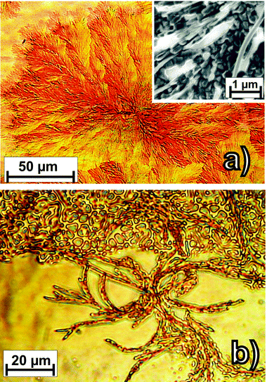 | ||
| Fig. 1 Optical micrographs of rubrene films (nominal thickness 40 nm) grown by OMBD at a rate of 25 Å min−1 and a substrate temperature of 375 K (a) on SiO2 and (b) on Au(111). The inset in (a) shows a SEM micrograph with the microstructure of the dendritic films on gold. | ||
To compensate the loss of rubrene through thermal desorption from the sample and/or the reduced sticking probability at elevated temperature a new hot wall-type evaporator has been designed. By bridging the gap between sample and evaporator cell with a separately heated glass tube a strongly enhanced rubrene vapor pressure in front of the surface is maintained. This allows deposition even at temperatures close to the sublimation point and hence enables growth under thermal equilibrium conditions. As shown by the micrographs depicted in Fig. 2 this deposition technique yields crystalline rubrene films. The average size of the crystallites depends on the actual growth temperature. While rather elongated crystals of about 0.3 μm × 1.5 μm are formed at 395 K larger crystallites with lateral dimensions of more than 25 μm are obtained upon growth at 415 K on SiO2. On Au(111) the latter growth conditions yielded rather laminar crystallites with diameters of up to 40 μm. A comparison of the characteristic oblique shape of the resulting crystallites with the orthorhombic crystal structure of rubrene15 indicates that they are (001)-oriented i.e. their surface consists of ab-planes. The homogeneous orientation of these crystallites on gold is further confirmed by polarization microscopy (Fig. 2d,f) which reveals a uniform switch of the polarization contrast within 1–2°. Tapping mode AFM measurements indicated that the individual crystallites have flat surfaces consisting of molecularly flat terraces extending over several hundred nanometres separated by monomolecular steps with a height of 1.5 ± 0.2 nm. This value is in close agreement with the (001)-layer spacing of d(001) = 1.34 nm in rubrene crystals (see Fig. 3c) and hence corroborates the crystalline orientation.
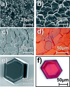 | ||
| Fig. 2 SEM and polarization micrographs of rubrene films grown by hot wall deposition at different temperatures onto SiO2 and Au(111) surfaces: (a) on SiO2 at 395 K, (b) on SiO2 at 415 K, (c), (d) on Au(111) at 415 K and (e), (f) on SiO2 at 423 K. | ||
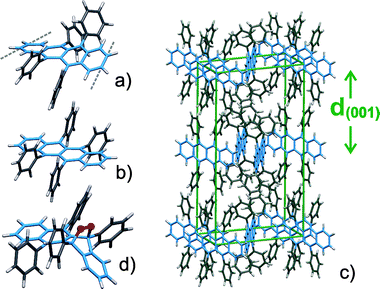 | ||
| Fig. 3 Molecular geometry of rubrene (a) in the gas phase and (b) in the crystalline phase together with (c) the rubrene crystal structure and (d) the molecular structure of rubreneperoxide. For better visualization of the molecular conformation and orientation the tetracene backbone is depicted in blue in the HTML version. | ||
When increasing the substrate temperature slightly to 423 K a different growth mode was observed and instead individual crystallites are formed. A comparison of the resulting crystals grown on both substrates shows that on SiO2 distinct perfectly shaped orthorhombic crystals with dimensions of up to 100 μm are formed (see Fig. 2e,f) while on gold a tendency of clustering of the crystals was observed. Interestingly, a quite different thermal stability has been obtained for the rubrene films prepared by OMBD and hot wall deposition. Whereas a complete thermal desorption of the amorphous films proceeds at temperatures below 416 K the crystalline films can be heated at 428 K for more than an hour without any noticeable loss of material. Compared to other organic semiconductor films the present growth properties appear to be somewhat surprising. For example in case of pentacene, a thoroughly-studied van der Waals-bond organic semiconductor with identical sublimation enthalpy (pentacene: 156.9 kJ mol−1, rubrene: 157.4 kJ mol−1), crystalline films with grain sizes of several micrometres can be grown by OMBD at room temperature.10,11 An important piece of information to unravel the rather different growth properties provides a closer inspection of the molecular structure of rubrene in its gas phase and crystal phase. Using density functional theory (DFT) the geometry of a free rubrene molecule has been calculated yielding D2 symmetry with a twisting of the tetracene-backbone of about 42° as shown in Fig. 3a) thus leading to an axial chirality. In contrast in the crystal phase15 rubrene adopts a conformation with planar tetracene backbone (C2h symmetry) without any chirality. Moreover, effective densities have been estimated from the van der Waals dimensions for both molecular conformations and yielded values of 1.38 g cm−3 for the planar geometry and 1.30 g cm−3 for the twisted geometry. The calculated energy difference of both molecular conformations amounts to 210 meV. In the crystalline phase this energy which is required for planarization of the backbone is compensated by the lattice energy. The results thus indicate that the thermal energy at room temperature is too small to activate the required conformational change and only results in rather amorphous films or the formation of nano-crystallites at elevated temperature. On the other hand the mobility of such nano-crystallites is too small to allow a formation of long range ordered crystalline films. This is in line with the outcome of a recent X-ray absorption study where evidence is found that the twisted geometry of the molecules is preserved for thin films and only above a critical film thickness a change of the molecular conformation takes place which enables the formation of nano-crystallites.16 We speculate that due to the high vapor pressure inside the hot wall evaporator a large number of many body collisions can occur which may assist a conformational change and therefore together with the higher mobility of the molecular entities allow a crystalline growth with long range ordering and a loss of chirality.
As regards the use of organic films for OFET devices a severe problem is their degradation e.g. through oxidation which leads to a reduction of the charge carrier mobility by several orders of magnitude.3,12 This issue is of particular importance for device processing and handling at ambient conditions but also in connection with crystal flip technique which has been used to study the electronic transport properties of molecular single crystals.4,8 To characterize the chemical stability of the present rubrene films their chemical composition after exposure to air has been analyzed by means of LDI-TOF mass spectroscopy. In addition to rubrene only rubreneperoxide17 was identified in the corresponding mass spectra. The quantitative analysis yielded rather different rubreneperoxide concentrations for the various films. Thin amorphous films with a thickness of less than 3 nm are found to oxidize completely upon exposure to air within a few minutes while rubrene crystallites grown by hot wall deposition appear rather inert. The latter analysis was possible by using a laser spot diameter of just a few micrometer which can be focused to individual crystallites. A more quantitative analysis was carried out by measuring the depth profile of the peroxide species for the various rubrene films after keeping them for a week under ambient conditions (without exposure to UV light). As shown in Fig. 4 for the amorphous and dendritic films large peroxide concentrations were found at the surface which reveal a slow decrease with increasing depths. In contrast for the crystallites much smaller peroxide contents were measured but reveal a non negligible amount of oxidation at their surface which needs to be considered when contacting such single crystals. Accompanied DFT calculations of the molecular geometry of rubreneperoxide yielded a bending of the last aromatic ring of the tetracene-backbone by 55° due to the oxygen as shown in Fig. 3d). A comparison of this structure with the molecular geometry and packing of rubrene in its crystal phase suggests that the oxidation of rubrene in single crystals is sterically hindered or requires a repacking. In contrast this reaction becomes possible in the rather loosely packed amorphous films which also provide diffusion channels for oxygen.
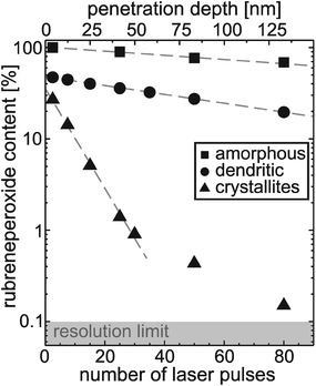 | ||
| Fig. 4 Depth profile of the rubreneperoxide concentration determined by LDI-TOF MS for the various rubrene films after exposure to air for about 1 week. | ||
In summary, it is demonstrated that using hot wall deposition, well-oriented crystalline films of rubrene can be grown which show high thermal and chemical stability and hence are promising for applications in organic electronics. Our inability to prepare crystalline films by OMBD is attributed to an activated conformational change of the molecular structure as compared to the gas phase which is accompanied by a loss of chirality. This property appears to be quite general in film growth of non-planar organic molecules which can adopt different molecular conformations in gas phase and crystalline phase. For example, in the case of para-phenylenes the free molecules reveal considerable twisting of the phenyl units while the molecules crystallize in a planar geometry. Regarding the growth of crystalline films with long range ordering this has only been achieved by hot wall deposition as reported e.g. for the case of para-sexiphenyl.18
Acknowledgements
The authors are grateful to Dr R. D. Neuser, Dr O. Medenbach and R. Breuckmann (University Bochum) for their assistance with SEM, polarization microscopy and LDI-TOF mass spectroscopy measurements and Prof. V. Staemmler (University Bochum) for his support with the calculations. D. K. acknowledges financial support from the Studienstiftung des Deutschen Volkes. This work has been funded by the German Research Council (DFG focus program OFET).References
- L. S. Hung and C. H. Chen, Mater. Sci. Eng. Rep., 2002, 39, 143 CrossRef.
- C. D. Dimitrakopoulos and P. R. L. Malenfant, Adv. Mater., 2003, 14, 99.
- N. Karl, in Organic Electronic Materials, ed. R. Frachioni and G. Grosso, Springer, Berlin 2001, p. 283 Search PubMed.
- R. W. I. de Boer, M. E. Gershenson, A. F. Morpurgo and V. Podzorov, Phys. Status Solidi A, 2004, 201, 1302 CrossRef CAS.
- G. Witte and Ch. Wöll, J. Mater. Res., 2004, 19, 1889 CrossRef CAS.
- H. Aziz and Z. D. Popovic, Appl. Phys. Lett., 2002, 80, 2180 CrossRef CAS.
- C. H. Chuen and Y. T. Tao, Appl. Phys. Lett., 2002, 81, 4499 CrossRef CAS.
- V. C. Sundar, J. Zaumseil, V. Podzorov, E. Menard, R. L. Willett, T. Someya, M. E. Gershenson and J. A. Rogers, Science, 2004, 303, 1644 CrossRef CAS.
- H. H. Fong, S. K. So, W. Y. Sham, C. F. Lo, Y. S. Wu and C. H. Chen, Chem. Phys., 2004, 298, 119 CrossRef CAS.
- C. D. Dimitrakopoulos, A. R. Brown and A. Pomp, J. Appl. Phys., 1996, 80, 2501 CrossRef CAS.
- G. Beernink, T. Strunskus, G. Witte and Ch. Wöll, Appl. Phys. Lett., 2004, 85, 398 CrossRef CAS.
- O. D. Jurchescu, J. Baas and T. T. M. Palstra, Appl. Phys. Lett., 2004, 84, 3061 CrossRef CAS.
- S. Lukas, S. Vollmer, G. Witte and Ch. Wöll, J. Chem. Phys., 2001, 114, 10123 CrossRef CAS.
- GAUSSIAN 98 (Revision A.11.1), Gaussian Inc., Pittsburgh PA, 2001 Search PubMed.
- I. V. Bulgarovskaya, V. M. Vozzhennikov, S. B. Aleksandrov and V. K. Belsky, Latv. PSR Zinat. Akad. Vestis, Kim. Ser., 1983, 4, 53 Search PubMed.
- D. Käfer, L. Ruppel, G. Witte and C. Wöll, submitted.
- R. M. Hochstrasser and M. Ritchie, Trans. Faraday Soc., 1956, 52, 1363 RSC.
- A. Andreev, G. Matt, C. J. Brabec, H. Sitter, D. Badt, H. Seyringer and N. S. Sariciftci, Adv. Mater., 2000, 12, 629 CrossRef CAS.
| This journal is © the Owner Societies 2005 |