Wafer-scale fabrication of periodic polymer attolitre microvial arrays
Peng
Jiang†
*
Corning Science & Technology, Corning Incorporated, Corning, NY 14831, USA
First published on 7th February 2005
Abstract
Wafer-size periodic polymer attolitre microvial arrays of varying depth have been fabricated by templating from spin-coated 2D non-close-packed colloidal crystal-polymer nanocomposites.
Arrays of microvials are of importance in the miniaturization of analytical and bioanalytical techniques.1–7 They allow isolating and handling small volumes of liquids, or even single cells and single molecules.1,4 Standard photolithography6 and soft lithography1 are suited for the fabrication of picolitre microwells. However, these processes are costly and tend to be limited by low resolution when the dimension of microvials is close to the diffraction limitation of photolithography.
Various non-lithographic templating alternatives have been developed to make periodic microvial arrays. Condensed water droplets in the breath figure method,8–10 rod–coil block copolymers,11,12 and two-dimensional (2D) ordered arrays of colloids13–20 have been used as templates. But, the replicated microwells are usually interconnected and post-treatments are needed to seal the interconnecting pores to reduce inter-vial interference.10,18 Additionally, these self-assembly techniques are not compatible with standard batch microfabrication, thus hindering mass-fabrication of practical microanalytical devices, such as microscale total analysis system (µTAS).21
Here we describe a simple and microfabrication-compatible non-lithographic approach for mass-fabricating wafer-size polymer attolitre microvial arrays. We use our recently developed spin-coating technique to make 2D colloidal crystal-polymer nanocomposites as templates.22 Ethoxylated trimethylolpropane triacrylate (ETPTA, SR 454, Sartomer) dispersions of monodisperse silica particles are spin-coated and subsequently photopolymerized to form 2D non-close-packed colloidal crystal-polymer nanocomposites. Wafer-scale (up to 6 inch in diameter) samples can be routinely made within twenty minutes.
Fig. 1 shows the schematic outline of the procedures for creating periodic microvial arrays by using spin-coated nanocomposites as templates. Oxygen plasma etching operating at 40 mTorr oxygen pressure, 100 sccm flow rate, and 100 W working power is carried out on a PlasmaTherm 790 (Unaxis) reactive ion etcher. Other more economic and simpler plasma etchers, such as Plasma-Prep II Plasma Etcher (SPI) for microscope sample preparation, can also be used to etch the top polymer layer. The etching depth can be easily controlled by adjusting the etching conditions and time. The typical etching rate for the conditions as described above using PlasmaTherm 790 is ≈150 nm min−1. The exposed silica spheres can then be dissolved in 2% hydrofluoric acid aqueous solution for several minutes, leaving behind 2D ordered polymer microvial arrays supported on silicon wafers. As silica spheres are not contacting in the original nanocomposite templates,22 the resulting microvials are separated from each other. This is an important advantage over other self-assembly approaches using close-packed spheres as templates, as no further steps are needed to form isolated microwells for potential microscale analytical applications.
 | ||
| Fig. 1 Schematic illustration of the experimental procedures for making periodic polymer microvial arrays by using 2D non-close-packed colloidal crystal-polymer nanocomposites as templates. | ||
Our approach allows for the rapid and large-scale fabrication of wafer-size periodic microwell arrays. Fig. 2A shows a photograph of a 4 inch diameter (81 cm2) polymer microvial arrays templated from 320 nm silica spheres under white light illumination. The sample exhibits striking six-arm diffraction with exact 60° angles between neighbouring arms, indicating wafer-scale hexagonal ordering of microwells.22,23 Different reflected colours are caused by different incident angles of the illuminating white light. To make a sample of such large area takes less than half an hour. This is another big advantage over previous colloidal-crystal-templated syntheses, as it may take days or even weeks for them to produce a centimetre-size crystalline template.24
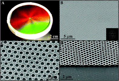 | ||
| Fig. 2 Wafer-size period microvial arrays. (A) Photograph of a 4 inch sample templated from 320 nm silica spheres illuminated with white light. (B) Typical top-view SEM image and its FFT of the sample shown in (A). (C) Higher magnification SEM image. (D) Side-view SEM image. | ||
The long-range hexagonal ordering of the microwells of the 4 inch sample is confirmed by the typical scanning electron microscope (SEM) image and its fast Fourier Transform (FFT) shown in Fig. 2B. Although there are defects, such as point defects and misalignment, the resultant 2D periodic void arrays cover the whole wafer area. From the higher magnification SEM image (Fig. 2C), it is clearly evident that the microvials are well separated and no interconnecting pores, which are characteristic for close-packed templates,10,25–28 are present. The centre-to-centre distance of neighbouring microvials (≈1.4D, where D is the diameter of the templating silica spheres) retains that of spin-coated nanocomposite templates.22 The smoothness of both the inner walls of the voids and the top polymer surface is also obvious from the SEM image. The depth of the microvials can be easily determined by side-view SEM as shown in Fig. 2D. In addition, the final voids are not through-pores, but having a thin (≈100 nm) backing layer between the substrate and the void arrays. Such backing layers have also been observed for thicker nanocomposites made by spin-coating.22
These 2D hexagonally ordered arrays of submicron voids can hold microscopic drops of liquids with volumes as small as ≈17 attolitres well−1 and the void density can be as high as ≈6 × 10⁸ wells cm−2. As the nanocomposite templates can be made from a wide range of particle diameters (from ≈100 nm to ≈2 µm) by the spin-coating technique,22 periodic arrays of microwells with volumes ranging from attolitre to femtolitre can be templated.
Another major merit of this technique is its compatibility with standard semiconductor microfabrication. The on-wafer planar configuration and the wafer-scale uniform thickness of the microvial arrays allow the construction of complex micropatterns with submicron resolution using photolithography and dry etching for potential microanalytical applications. Fig. 3A shows a patterned ETPTA microvial arrays. 2 µm thick AZ 5214E photoresist (Clarian) is used as the etching mask. The PlasmaTherm 790 etcher operating at the same conditions as described above is used to remove unprotected portions of the ETPTA arrays. The higher magnification SEM image in Fig. 3B reveals the good definition of a 16 µm wide line and the preservation of the hexagonal ordering and the centre-to-centre distance of the microvials during the entire patterning process.
 | ||
| Fig. 3 Micropatterned periodic microvial arrays. (A) Low magnification SEM image. (B) Higher magnification SEM image showing a single 16 µm wide line that is a portion of the bottom double-line pattern in (A). | ||
Herein, wafer-scale microvial arrays are made out of ETPTA, which has similar chemical properties to poly(methyl methacrylate) and is chemical and water resistant. The polymer surface can be functionalized to facilitate the covalent coupling of different species.29 By modifying the surface of silica colloids using organosilane agents to make stable colloid/monomer dispersions,30 the as-described spin-coating and oxygen plasma etching processes can be used to fabricate microvial arrays from a large variety of polymeric materials, such as PMMA, polystyrene and polyurethane etc.
In summary, we have developed a non-lithographic procedure for mass-fabricating wafer-size polymer microvoid arrays, with volumes ranging from femtolitres well−1 to attolitres well−1 and densities as high as 109 wells cm−2. 2D ordered non-close-packed colloidal crystal-polymer nanocomposites made by spin-coating are used as templates in fabricating isolated microvials. The opening and the depth of the microvials can be easily adjusted by controlling the oxygen plasma etching conditions. The technique is compatible with standard semiconductor microfabrication and complex micropatterns can be created by photolithography and dry etching for potential microanalytical applications, such as microscale total analytical system (µTAS).
The author would like to thank Dr Lawrence W. Shacklette, Dr Macrae Maxfield, and Dr Michael J. McFarland of Corning Polymer Photonics for many useful discussions and support.
Notes and references
- R. J. Jackman, D. C. Duffy, E. Ostuni, N. D. Willmore and G. M. Whitesides, Anal. Chem., 1998, 70, 2280 CrossRef CAS.
- B. A. Grzybowski, R. Haag, N. Bowden and G. M. Whitesides, Anal. Chem., 1998, 70, 4645 CrossRef CAS.
- R. A. Clark, P. B. Hietpas and A. G. Ewing, Anal. Chem., 1997, 69, 259 CrossRef CAS.
- D. T. Chiu, C. F. Wilson, F. Ryttsen, A. Stromberg, C. Farre, A. Karlsson, S. Nordholm, A. Gaggar, B. P. Modi, A. Moscho, R. A. Garza-Lopez, O. Orwar and R. N. Zare, Science, 1999, 283, 1892 CrossRef CAS.
- J. M. Cooper, Trends Biotechnol., 1999, 17, 226 CrossRef CAS.
- A. L. Grosvenor, A. Feltus, R. C. Conover, S. Daunert and K. W. Anderson, Anal. Chem., 2000, 72, 2590 CrossRef CAS.
- C. C. Meek and P. Pantano, Lab Chip, 2001, 1, 158 RSC.
- M. Srinivasarao, D. Collings, A. Philips and S. Patel, Science, 2001, 292, 79 CrossRef CAS.
- L. Song, R. K. Bly, J. N. Wilson, S. Bakbak, J. O. Park, M. Srinivasarao and U. H. F. Bunz, Adv. Mater., 2004, 16, 115 CrossRef CAS.
- B. Erdogan, L. L. Song, J. N. Wilson, J. O. Park, M. Srinivasarao and U. H. F. Bunz, J. Am. Chem. Soc., 2004, 126, 3678 CrossRef CAS.
- S. A. Jenekhe and X. L. Chen, Science, 1999, 283, 372 CrossRef CAS.
- G. Widawski, M. Rawiso and B. Francois, Nature, 1994, 369, 387 CrossRef CAS.
- P. Jiang, Angew. Chem., Int. Ed., 2004, 43, 5625 CrossRef CAS.
- D. G. Choi, S. G. Jang, H. K. Yu and S. M. Yang, Chem. Mater., 2004, 16, 3410 CrossRef CAS.
- J. E. Barton and T. W. Odom, Nano Lett., 2004, 4, 1525 CrossRef CAS.
- F. Q. Sun, W. P. Cai, Y. Li, B. Q. Cao, Y. Lei and L. D. Zhang, Adv. Funct. Mater., 2004, 14, 283 CrossRef CAS.
- M. Kanungo and M. M. Collinson, Chem. Commun., 2004, 548 RSC.
- M. E. Abdelsalam, P. N. Bartlett, J. J. Baumberg and S. Coyle, Adv. Mater., 2004, 16, 90 CrossRef CAS.
- P. N. Bartlett, J. J. Baumberg, S. Coyle and M. E. Abdelsalam, Faraday Discuss., 2004, 125, 117 RSC.
- J. C. Garno, N. A. Amro, K. Wadu-Mesthrige and G. Y. Liu, Langmuir, 2002, 18, 8186 CrossRef CAS.
- Micro Total Analytical Systems, ed. A. van den Berg and P. Bergveld, Kluwer Academic Publishers, Dordrecht, 1995 Search PubMed.
- P. Jiang and M. J. McFarland, J. Am. Chem. Soc., 2004, 126, 13778 CrossRef CAS.
- R. L. Hoffman, Trans. Soc. Rheol., 1972, 16, 155 Search PubMed.
- P. Jiang, J. F. Bertone, K. S. Hwang and V. L. Colvin, Chem. Mater., 1999, 11, 2132 CrossRef CAS.
- Y. A. Vlasov, X. Z. Bo, J. C. Sturm and D. J. Norris, Nature, 2001, 414, 289 CrossRef CAS.
- Y. N. Xia, B. Gates, Y. D. Yin and Y. Lu, Adv. Mater., 2000, 12, 693 CrossRef CAS.
- A. Blanco, E. Chomski, S. Grabtchak, M. Ibisate, S. John, S. W. Leonard, C. Lopez, F. Meseguer, H. Miguez, J. P. Mondia, G. A. Ozin, O. Toader and H. M. van Driel, Nature, 2000, 405, 437 CrossRef CAS.
- P. Jiang, K. S. Hwang, D. M. Mittleman, J. F. Bertone and V. L. Colvin, J. Am. Chem. Soc., 1999, 121, 11630 CrossRef CAS.
- J. Y. Cheng, C. W. Wei, K. H. Hsu and T. H. Young, Sens. Actuators, B, 2004, 99, 186 CrossRef.
- A. P. Philipse and A. J. Vrij, J. Colloid Interface Sci., 1989, 128, 121 CrossRef CAS.
Footnote |
| † Current address: Department of Chemical Engineering, Princeton University, Princeton, NJ 08544, USA. E-mail: pjiang@princeton.edu; Fax: 609-258-6835; Tel: 609-258-1561. |
| This journal is © The Royal Society of Chemistry 2005 |