DOI:
10.1039/B105644C
(Paper)
J. Mater. Chem., 2002,
12, 86-91
Sol–gel deposition and luminescent properties of oxyapatite Ca2(Y,Gd)8(SiO4)6O2 phosphor films doped with rare earth and lead ions
Received
27th June 2001
, Accepted 8th October 2001
First published on 26th November 2001
Abstract
Rare-earth and lead ions (Eu3+, Tb3+, Dy3+, Pb2+) doped Ca2Y8(SiO4)6O2 and Ca2Gd8(SiO4)6O2 thin films have been dip-coated on silicon and quartz glass substrates through the sol–gel route. X-Ray diffraction (XRD), TG–DTA, scanning electron microscopy (SEM), atomic force microscopy (AFM), FT-IR and luminescence excitation and emission spectra as well as luminescence decays were used to characterize the resulting films. The results of XRD reveal that these films remain amorphous below 700![[thin space (1/6-em)]](https://www.rsc.org/images/entities/char_2009.gif) °C, begin to crystallize at 800°C and crystallize completely around 1000°C with an oxyapatite structure. The grain structure of the film can be seen clearly from SEM and AFM micrographs, where particles with various
shapes and average size of 250 nm can be resolved. Eu3+ and Tb3+ show their characteristic red (5D0–7F2) and green (5D4–7F5) emission in the films with a quenching concentration of 10 and 6 mol%
(of Y3+), respectively. The lifetime and emission intensity of Eu3+ increase with the temperature treatment from 700 to 1100°C, while those of Tb3+ show a maximum at 800°C. Energy transfer phenomena have been observed by activating the oxyapatite film host-lattice Ca2Gd8(SiO4)6O2 with Tb3+
(Dy3+). In addition, Pb2+ can sensitize the Gd3+ sublattice in Ca2Gd8(SiO4)6O2.
°C, begin to crystallize at 800°C and crystallize completely around 1000°C with an oxyapatite structure. The grain structure of the film can be seen clearly from SEM and AFM micrographs, where particles with various
shapes and average size of 250 nm can be resolved. Eu3+ and Tb3+ show their characteristic red (5D0–7F2) and green (5D4–7F5) emission in the films with a quenching concentration of 10 and 6 mol%
(of Y3+), respectively. The lifetime and emission intensity of Eu3+ increase with the temperature treatment from 700 to 1100°C, while those of Tb3+ show a maximum at 800°C. Energy transfer phenomena have been observed by activating the oxyapatite film host-lattice Ca2Gd8(SiO4)6O2 with Tb3+
(Dy3+). In addition, Pb2+ can sensitize the Gd3+ sublattice in Ca2Gd8(SiO4)6O2.
Luminescent thin films have been attracting much attention for their potential application in high-resolution devices such as cathode ray tubes (CRTs), flat panel display devices and field emission displays (FEDs).1–3 Compared with conventional display screens prepared by deposition of fine grain luminescent powders, displays with thin film phosphors have higher contrast, superior thermal conductivity as well as a high degree of uniformity and better adhesion.4 In addition, the uniform thickness combined with smoother surface morphology and smaller grain size make it possible to obtain smaller pixel spot sizes to achieve a higher resolution.5 Efforts have been made in the past decade to develop various types of luminescent films via the sol–gel method. Representative examples are Y2SiO5∶Tb6
and Y3Al5O12∶Tb7 films for cathodoluminescence, Y3Al5O12∶Eu8 and Y3(Al, Ga)5O12∶Tb9 films for field emission displays, Y2O3∶Eu,10 TiO2∶Eu11 and Zn2SiO4∶Mn/Tb12,13 films for photoluminescence, and ZnS∶Mn/Tb14 and Ga2O3∶Eu/Mn15 films for electroluminescence. However, so far the total number of publications in this field has not been over twenty. Recently we have published a review concerning the progress of luminescent films fabricated via the sol–gel method.16
Ca2RE8(SiO4)6O2
(RE = Y or Gd) are ternary rare-earth-metal silicates with oxyapatite structure, which have been used as host materials for the luminescence of various rare earth and mercury-like ions.17–20 The most prominent structural characteristic is the two rare-earth sites in the oxyapatite host lattice, i.e., the nine-coordinate 4f site with C3 point symmetry and the seven-coordinate 6h site with Cs point symmetry. Both sites are very suitable for the luminescence of rare earth ions due to their low symmetry features.17–20 So far no report has been published on luminescent films based on these materials. In order to emphasize the significance of luminescent films prepared by the sol–gel method, we report the structural
and luminescent properties of rare earth (Eu3+, Tb3+) and lead ions (Pb2+)-doped oxyapatite Ca2RE8(SiO4)6O2
(RE = Y or Gd) films deposited by this method.
Experimental
The starting materials used for preparation of the phosphor films were CaCO3
(A.R), Y2O3
(99.99%), Eu2O3
(99.99%), Tb4O7
(99.99%), Dy2O3
(99.99%), Pb(NO3)2
(A.R), Gd2O3
(99.99%) and tetraethoxysilane Si(OC2H5)4
(TEOS). The preparation of the samples consists of three steps: synthesis of the coating solution, film deposition, and subsequent heat treatment.
Synthesis of the coating solutions
The preparation of the coating solutions is as follows. First, stoichiometric amounts of the starting materials were dissolved in dilute HNO3; second, a suitable amount of ethanol was added to this solution under stirring until a homogeneous phase formed; third, a stoichiometric amount of TEOS dissolved in ethanol was added to the above solution with magnetic stirring at room temperature, and the pH value of this solution was kept between one and three. The obtained sol which was highly transparent and remained stable for several weeks if sealed, was then ready for film deposition.
Film deposition
The substrates (quartz glasses and silicon wafers) were pre-cleaned in a 5 wt% KOH ethanol solution for fifteen minutes, followed by a five-minute dipping in 1 M HCl to neutralize the alkali attack on the glass surface, and then soaked in pure water for twenty minutes. Finally they were thoroughly ultrasonicated in ethanol for twenty minutes. The cleaned substrates were then dipped into the coating solution before being slowly withdrawn from the solution with a speed of 0.5 cm s−1. Samples were then baked at 120°C for 5 h immediately after coating. The dried films were then annealed to 500°C for 2 h in a furnace with a heating rate of 60°C h−1. The preheated film samples were then fired at a rate of 100°C h−1 to the desired temperature (700–1100°C) and held at this temperature for 2 h.
Characterization
X-Ray diffraction (XRD) patterns of the film samples were recorded on a Rigaku-Dmax 2500 diffractometer using Cu Kα radiation (λ = 0.15405 nm). FT-IR spectra were measured on a Perkin-Elmer 580B infrared spectrophotometer using the KBr pellet technique. A DT-30 Shimadzu thermal analyzer was used for recording TGA–DTA curves of the gel powders. The morphology of crystalline film samples were inspected using a scanning electron microscope (JEOL JXA-840) and an atomic force microscope (AFM, Seiko) in tapping mode. Excitation and emission spectra were obtained on a SPEX FL-2T2 spectrofluorometer equipped with a 450 W xenon lamp as the excitation source. Luminescence lifetimes were measured with a SPEX 1934D phosphorimeter using a 7 W pulse xenon lamp as the excitation source with a pulse width of 3 µs. All measurements were performed at room temperature (RT).
Results and discussion
Formation process and morphology of the phosphor films
XRD.
Fig. 1 shows XRD patterns of film samples annealed at different temperatures from 700 to 1100°C at intervals of 100°C. For films annealed below 700°C, no diffraction peaks are observed except for a broad band at 2θ = 22°, ascribed to quartz glass substrate. This indicates that the film remains amorphous below this temperature. For the sample fired at 800°C, a weak and broad peak at 2θ = 29.8° is present in the XRD pattern, which is assigned to (210) reflection of oxyapatite Ca2Y8(SiO4)6O2, suggesting the starting of crystallization at this stage. At 900°C, other diffraction peaks at 2θ = 22.6°
(200), 23.7°
(111), 26.9°
(002),
29.1°
(102), 32.7°
(211) 33.3°
(112) and 33.8°
(300) belonging to crystalline oxyapatite are observed (JCPDS Card 27-93). These diffraction peaks increase in intensity with further increase of the annealing temperature, and no difference in width and intensity is observed for the 1000°C and 1100°C sintered samples, indicating that the crystallization of Ca2Y8(SiO4)6O2 is complete at 1000°C. This temperature is about 300°C lower than that of the powder Ca2Y8(SiO4)6O2 sample prepared by solid state reaction of carbonate and oxides, thus illustrating the advantage of the sol–gel method.21
 |
| | Fig. 1
XRD patterns of Ca2Y7.2Eu0.8(SiO4)6O2 films on quartz glass after heat treatment at different temperatures.
| |
TG–DTA.
The thermogravimetric and differential thermal analysis (TG–DTA) curves of the gel sample dried at 70°C are shown in Fig. 2. The gel sample shows rapid weight loss around 140°C, with endothermic peaks at 119 and 152°C, which result from the evaporation of residual water and ethanol in the powder gel. The endothermic peaks at 325 and 455°C correspond to the decomposition of the organic compounds and nitrates in the gel. No weight loss occurs beyond 500°C. The exothermic peak at 915°C is due to the crystallization of the gel, agreeing well with the results of XRD analysis.
 |
| | Fig. 2
TGA–DTA curves of the dry gel powder obtained from the coating sol.
| |
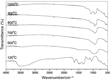
FT-IR spectra.
FT-IR spectra were recorded for the films on silicon wafers at various stages of heat treatment, as shown in Fig. 3. For the gel film after heat treatment at 120°C, the IR spectrum shows three main regions of interest: the first (a broad band) in the range 2750–3750 cm−1 with a maximum at 3488 cm−1, arises from the absorption of O–H groups; the second region in the range 1250–1750 cm−1, which originates from the absorption of H2O (1640 cm−1) and NO3− groups (1480, 1320 cm−1); and the third region with peaks at 1000–1170 cm−1, which are assigned to the absorption of Si–O–Si asymmetric stretching vibrations. Significant changes are observed with
further heat treatment. After heating at 500°C, the absorption peaks from –OH, H2O and NO3− almost disappear, and a new broad absorption band peaking at 950 cm−1 is present, which arises from the asymmetric stretching vibration of SiO4 groups. After heat treatment at 700°C, the absorption of H2O and NO3− disappear completely, indicating the complete evaporation of H2O and the pyrolysis of nitrate; meanwhile, a new absorption peak at 553 cm−1 due to bending vibration of O–Si–O bonds is present, and the absorption bands of SiO4 groups remain broad implying the amorphous character of the film. Heat treatment between 800 to 1000°C leads the absorption peaks of SiO4 to be more structured, suggesting that crystallized silicate oxyapatite has formed in the film. Note that the
broad absorption peak at 1076 cm−1 becomes stronger with increasing the heat treatment temperature after 900°C. In fact, in the IR spectrum of pure silicon wafer without any film, this peak also exists and its intensity increases with raising the treatment temperature. Therefore, this peak can be attributed to the absorption of Si–O–Si bonds in SiO2, which formed on the surface of the silicon wafer due to the oxidation of silicon at high temperatures.
Morphology of the films.
The morphology of a Ca2Y8(SiO4)6O2∶Eu film deposited on quartz glass was investigated by SEM and AFM. The grain structure of the film can be seen clearly from SEM and AFM. The SEM images of the surface and cross-section of an opaque Ca2Y8(SiO4)6O2∶Eu film sintered at 1000°C are shown in Fig. 4(a) and (b), respectively. From the surface image of the film we can observe that the film consists of fine closely packed particles with an average size of 250 nm (Fig. 4(a)). From the SEM image for the cross-section of the film (Fig. 4(b)) it is evident that the film is uniform in thickness, ca. 2.66 µm.
The surface morphology can be observed more clearly by AFM as shown in Fig. 5, where different shapes ( triangular, spherical etc.) of particles can be resolved.
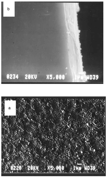 |
| | Fig. 4
SEM images of the surface (a) and cross-section (b) of a Ca2Y7.2Eu0.8(SiO4)6O2 film sintered at 1000°C.
| |
 |
| | Fig. 5
AFM image of Ca2Y7.2Eu0.8(SiO4)6O2 film sintered at 1000°C.
| |
Photoluminescence properties.
The photoluminescence properties of the films were studied by excitation and emission spectra as well as luminescence decays.
Ca2Y8(SiO4)6O2∶Eu3+ films.
Fig. 6 shows the excitation and emission spectra for Ca2Y7.2Eu0.8(SiO4)6O2 films. The excitation spectrum (Fig. 6(a)) consists of a broad intense band with a maximum at 269 nm and some weak lines. The former is due to the charge transfer band (CTB) of Eu3+–O2−, and the latter are from the f–f transitions within the Eu3+ 4f6 electron configuration. The emission spectra were recorded as a function of annealing temperature (Fig. 6(b)). Upon excitation into the CTB at 269 nm, all the emission spectra are composed of 5D0–7FJ
(J = 1,
2, 3, 4) emission lines of Eu3+, with the hypersensitive red emission transition 5D0–7F2
(616 nm) being the most prominent group, agreeing well with the low local symmetry (C3 and/or Cs) for Eu3+ in the host lattice. Influenced by the background of the films, i.e. non-crystalline silica glass substrate, the spectral bands of Eu3+ seem to be broader than those in the crystalline powders, and the 5D0–7F0 transition line of Eu3+ is hidden by the broad 5D0–7F1 transition band.17 In addition, no emission from higher 5DJ
(J > 0) levels is observed. This can be ascribed to the fact that the energy gaps between 5D2
and 5D1 and between 5D1 and 5D0 of Eu3+ are 2500 and 1750 cm−1 respectively, and so silicate groups with a maximum vibration energy of 950 cm−1 (evidenced by FT-IR spectra in Fig. 3) are able to bridge the gaps between the higher lying levels of the Eu3+ and the 5D0 level.17 With the increase of annealing temperature, the Eu3+ emission intensity increases and more spectral lines can be resolved. This is in accord with the fact that the crystallinity of the film increases with firing temperature, as shown in the XRD patterns (Fig. 1).
 |
| | Fig. 6
Excitation (a) and emission (b) spectra of Ca2Y7.2Eu0.8(SiO4)6O2 films (annealed at various temperatures for emission).
| |
Photoluminescence decay curves of Eu3+ in Ca2Y7.2Eu0.8(SiO4)6O2 films sintered at various temperatures are shown in Fig. 7. In general, all these curves can be well fitted to a single exponential function as I = I0 + Aexp[−(t − t0)/τ]
(A is constant, τ is the lifetime), from which the lifetimes of Eu3+ are determined and shown in Fig. 7. It is found that the lifetime of Eu3+ increases with the annealing temperature. This is due to the fact that the content of impurities in the film such as –OH, –OR, H2O, NO3−etc. decreases
with increase of annealing temperature. The quenching of the luminescence of Eu3+ by excitation of the vibrations of these impurities decreases, resulting in the increase of the lifetimes of Eu3+. In addition, the lifetimes of Eu3+ have also been studied as a function of Eu3+ doping concentration in the films, as shown in Fig. 8. The lifetimes of Eu3+ first increase with dopant concentration, reaching a maximum at 10 mol%, and then decrease with further increasing the dopant concentration. This indicates concentration quenching of the luminescence of Eu3+ in the film host. The optimum concentration of Eu3+ is 10 mol% that of Y3+ in the Ca2Y8(SiO4)6O2 host film.
 |
| | Fig. 7
Decay curves of Eu3+ luminescence in Ca2Y7.2Eu0.8(SiO4)6O2 thin films annealed at different temperatures. The values of lifetimes are indicated.
| |
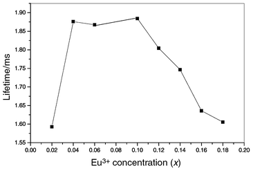 |
| | Fig. 8
Lifetimes of Eu3+ luminescence as a function of its doping concentration (x) in Ca2Y8(1 − x)Eu8x(SiO4)6O2 films.
| |
Ca2Y8(SiO4)6O2∶Tb3+ films.
Fig. 9 shows the excitation and emission spectra of a Ca2Y7.84Tb0.16(SiO4)6O2 thin film. The excitation spectrum (Fig. 9(a)) of Tb3+ contains an intense broad band with a maximum at 246 nm with a shoulder at 277 nm and some weak excitation lines in the longer wavelength region within the Tb3+ 4f8 electron configuration. The strong excitation band at 246 nm is due to the spin-allowed 4f8–4f75d transition (ΔS = 0) and the shoulder is from the spin-forbidden component of 4f8–4f75d transition (ΔS = 1),
respectively.18 Excitation into the spin-allowed 4f8–4f75d band at 246 nm yields the characteristic blue and green emission lines of Tb3+5D3, 4–7FJ
(J = 3, 4, 5, 6) transitions, with the 5D4–7F5
(545 nm) green emission as the most prominent feature (Fig. 9(b)). Due to the cross-relaxation betwwen 5D3–5D4 and 7F0–7F6, the blue emission of 5D3–7FJ transition is weak.
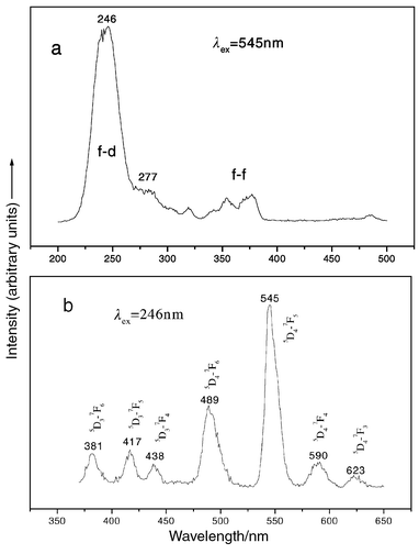 |
| | Fig. 9
Excitation (a) and emission (b) spectra of a Ca2Y7.84Tb0.16(SiO4)6O2 film.
| |
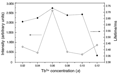
Fig. 10 shows the dependence of the intensity of Tb3+5D4–7F5 green emission and the lifetimes of the Tb3+5D4 excited state on its concentration (x) in Ca2Y8(1 − x)Tb8x(SiO4)6O2 films. Both the emission intensity and lifetimes of Tb3+ first increase with its doping concentration, reaching a maximum at x = 6 mol%, and then decrease with increasing Tb3+ concentration due to concentration quenching. Thus the optimum concentration for the Tb3+ green emission is 6 mol% that of Y3+ in Ca2Y8(SiO4)6O2 films.
 |
| | Fig. 10
Dependence of the relative emission intensity and lifetimes of Tb3+ luminescence on its doping concentration (x) in Ca2Y8(1 − x)Tb8x(SiO4)6O2 films.
| |
Furthermore, the lifetimes (5D4) and emission intensity of Tb3+(5D4–7F5) have also been studied as a function of the annealing temperature for the Ca2Y7.84Tb0.16(SiO4)6O2 film, as shown in Fig. 11. Differently from the results obtained with Eu3+
(the lifetime and emission intensity increase with an increase of the annealing temperature), both the Tb3+ lifetimes and emission intensity first increase sharply from 700 to 800°C and then decrease sharply above 900°C. This is because the Tb3+ is easily oxidized to Tb4+ at high temperature, with the latter acting as a quenching center for the luminescence of Tb3+.
 |
| | Fig. 11
Lifetimes and emission intensity of Tb3+ luminescence in Ca2Y7.84Tb0.16(SiO4)6O2 thin films as a function of annealing temperatures.
| |
Ca2Gd8(SiO4)6O2∶Pb2+, Tb3+
(Dy3+) films.
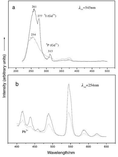
For comparison purposes, we also prepared Tb3+ and Pb2+-codoped Ca2Gd8(SiO4)6O2 films on quartz glass substrates. Under 254 nm excitation, the film shows bright green emission. Fig. 12 shows the excitation and emission spectra of Tb3+ and Pb2+-codoped Ca2Gd8(SiO4)6O2 and Ca2Y8(SiO4)6O2 thin films. The excitation spectrum of Tb3+- and Pb2+-codoped Ca2Gd8(SiO4)6O2 film consists of a strong absorption
band with a maximum at 261 nm, which corresponds to the Pb2+1S0–3P1 transition, followed by Gd3+8S–6I and 8S–6P transitions peaking at 277 and 313 nm, respectively. The presence of both Pb2+ and Gd3+ excitation indicates that energy transfer processes Pb2+–Tb3+ and Gd3+–Tb3+ occur in this film. Upon excitation into Pb2+ at 254 nm, the emission spectrum consists of a very weak Pb2+ emission band (background in the blue region) and a strong emission of Tb3+ with a maximum at 545 nm. However, energy transfer from Pb2+ to Tb3+ is far from complete at identical Pb2+ and Tb3+ concentrations for the Ca2Y8(SiO4)6O2
film. The emission intensity of Tb3+ in Ca2Gd8(SiO4)6O2 film is more than twice as strong as that in Ca2Y8(SiO4)6O2 under excitation into Pb2+ at 254 nm. Thus the role of Gd3+ as an intermediate in the energy transfer process from Pb2+ to Tb3+ is clearly seen, i.e., an energy migration process Pb2+–Gd3+–(Gd3+)n–Tb3+ occurs in the Ca2Gd8(SiO4)6O2 film. Dy3+ and Pb2+-codoped Ca2Gd8(SiO4)6O2 and Ca2Y8(SiO4)6O2 thin films were also prepared
on quartz glass, and showed similar behavior as above. These results for the film samples are similar to those obtained for powder samples of Pb2+ and Mn2+-codoped Sr2Gd8(SiO4)6O2.22
 |
| | Fig. 12
Excitation (a) and emission (b) spectra of Ca1.96Pb0.04RE7.9Tb0.1(SiO4)6O2
(RE = Gd; Y) thin films: (—) RE = Gd; (– – –) RE = Y.
| |
Conclusions
Luminescent thin films Ca2Y8(SiO4)6O2 and Ca2Gd8(SiO4)6O2 doped with rare earth and Pb2+ ions can be successfully deposited on quartz glass and silicon wafers by the sol–gel dip coating method. The films are uniform and crack free. They contain grains with an average size of 250 nm. From 700 to 1100°C, the lifetimes and emission intensity of Eu3+ increase with the annealing temperature, while those of the Tb3+ show a maximum at 800°C. The optimum concentrations of Eu3+ and Tb3+ in Ca2Y8(SiO4)6O2 films are 10 and 6 mol% of Y3+, respectively. The Pb2+ can sensitize the Gd3+-sublattice in Ca2Gd8(SiO4)6O2
films and enhance greatly the emission intensity of the codoped rare earth ions (Tb3+, Dy3+).
Acknowledgements
This project is financially supported by the foundation of “Bairen Jihua”of Chinese Academy of Sciences, the Outstanding Youth Fund of Jilin Province, and Personnel Ministry as well as Educational Ministry of China.
References
- X. Ouyang, A. H. Kitai and T. Xiao, J. Appl. Phys., 1997, 71, 404.
- G. A. Hirata, J. Mckittrick, M. Avalos-Borja, J. M. Siquetros and D. Devlin, Appl. Surf. Sci., 1997, 113/114, 509 CrossRef CAS.
- S. L. Jones, D. Kumar, R. K. Singh and P. H. Holloway, Appl. Phys. Lett., 1997, 71, 404 CrossRef CAS.
- L. Z. Meznar, B. Pracek, B. Orel and P. Bukovec, Thin Solid Films, 1998, 317, 336 CrossRef CAS.
- C. Feldman and M. O'Hara, J. Opt. Soc. Am., 1957, 47, 300 Search PubMed.
- E. M. Rabinovich, J. Shmulovich, V. J. Fratello and N. J. Kopyov, Am. Ceram. Soc. Bull., 1987, 6, 1505 Search PubMed.
- J. Y. Choe, D. Ravichandran, S. M. Biomquist, D. C. Morton, K. W. Kirchner, M. H. Ervin and U. Lee, Appl. Phys. Lett., 2001, 78, 3800 CrossRef CAS.
- D. Ravichandran, R. Roy, A. G. Chakhovsoi, C. E. Hunt, W. B. White and S. Erdei, J. Lumin., 1997, 71, 291 CrossRef CAS.
- S. Chadha and J. J. Alwan, US Pat., 1995, 5695809 Search PubMed.
- P. Rao, Solid State Commun., 1996, 99, 439 CrossRef.
- A. Conde-Gallardo, M. Garcia-Rocha, I. Hemandez-Calderon and R. Palomino-Merino, Appl. Phys. Lett., 2001, 78, 3436 CrossRef CAS.
- J. Lin, D. U. Saenger, M. Mennig and K. Baerner, Mater. Sci. Eng. B, 1999, 64, 73 Search PubMed.
- H. X. Zhang, C. H. Kam, Y. Zhou and X. Q. Han, Thin Solid Films, 2000, 370, 50 CrossRef CAS.
- W. Tang and D. C. Cameron, Thin Solid Films, 1996, 280, 221 CrossRef CAS.
- T. Minami, T. Miyata, T. Shirai and T. Nakatani, Mater. Res. Soc. Symp. Proc., 2000, 621, Q431 Search PubMed.
- J. Lin, M.
L. Pang, Y. H. Han, Y. H. Zhou, M. Yu and H. J. Zhang, Chin. J. Inorg. Chem., 2001, 17, 153 Search PubMed.
- J. Lin and Q. Su, Mater. Chem. Phys., 1994, 38, 98 CrossRef CAS.
- J. Lin and Q. Su, J. Mater. Chem., 1995, 5, 1151 RSC.
- M. J. J. Lammers and G. Blasse, J. Electrochem. Soc., 1987, 134, 2068 CAS.
- J. Lin and Q. Su, Phys. Status Solidi B, 1996, 196, 261 CAS.
- T. J. Isaacs, J. Electrochem. Soc., 1973, 120, 654 CAS.
- H. S. Kiliaan and G. Blasse, J. Electrochem. Soc., 1989, 136, 562 CAS.
|
| This journal is © The Royal Society of Chemistry 2002 |
Click here to see how this site uses Cookies. View our privacy policy here.