
Using hematite for photoelectrochemical water splitting: a review of current progress and challenges
Andebet Gedamu
Tamirat
a,
John
Rick
a,
Amare Aregahegn
Dubale
a,
Wei-Nien
Su
 b and
Bing-Joe
Hwang
*ac
b and
Bing-Joe
Hwang
*ac
aNanoElectrochemistry Laboratory, Department of Chemical Engineering, National Taiwan University of Science and Technology, Taipei, 106, Taiwan. E-mail: bjh@mail.ntust.edu.tw; Fax: +886-2-27376644
bNanoElectrochemistry Laboratory, Graduate Institute of Applied Science and Technology, National Taiwan University of Science and Technology, Taipei 106, Taiwan
cNational Synchrotron Radiation Research Center, Hsinchu, 30076, Taiwan
First published on 4th February 2016
Abstract
Photoelectrochemical (PEC) water splitting is a promising technology for solar hydrogen production to build a sustainable, renewable and clean energy economy. Hematite (α-Fe2O3) based photoanodes offer promise for such applications, due to their high chemical stability, great abundance and low cost. Despite these promising properties, progress towards the manufacture of practical water splitting devices has been limited. This review is intended to highlight recent advancements and the limitations that still hamper the full utilization of hematite electrodes in PEC water splitting systems. We review recent progress in manipulating hematite for PEC water splitting through various approaches, focused on e.g. enhancing light absorption, water oxidation kinetics, and charge carrier collection efficiency. As the morphology affects various properties, progress in morphological characterization from thicker planar films to recent ultrathin nanophotonic morphologies is also examined. Special emphasis has been given to various ultrathin films and nanophotonic structures which have not been given much attention in previous review articles.
1. Introduction
Photoelectrochemical (PEC) water splitting using semiconductor electrodes has received much attention and is considered to be the “holy grail” of solar energy conversion and storage revolution. However, most PEC water splitting systems that have been exploited so far have faced numerous challenges. Hematite (α-Fe2O3) based photoelectrodes have been intensively studied on account of hematite's abundance, non-toxicity, high photochemical stability, and narrow bandgap (1.9–2.2 eV). With a band gap of 2.1 eV hematite can achieve a theoretical maximum solar-to-hydrogen (STH) efficiency of 15%, which exceeds the STH benchmark efficiency of 10% required for practical applications. However, the practical maximum efficiency is still far from both the benchmark and theoretical maximum STH efficiencies. Several reviews have been published highlighting significant achievements in hematite photoanode performance using various approaches. For example in 2011 Grätzel's group presented a review focusing on new insights into its basic properties, attractive aspects, and the challenges in using it for photoelectrochemical (PEC) water splitting.1 A year later, Wheeler et al. provided another review dealing with progress towards the synthesis and characterization of nanostructured hematite, with an emphasis on charge carrier dynamics and photoelectrochemical properties.2 In this review, we aim to present the research effort made in recent years, with a view to providing up-to-date approaches and inspiring new ideas for tackling the remaining challenges. Starting with a brief introduction, first, we briefly discuss important recent progress in morphology determination and its relationship with the material's resulting properties, e.g. light absorption, water oxidation kinetics, and charge carrier collection, and progress in morphology from thicker planar films to recent ultrathin nanophotonic morphologies is examined. Special emphasis is given to ultrathin film approaches which offer the promise of improving the tradeoff between the poor carrier collection and the poor light absorption of hematite. The poor oxygen evolution reaction kinetics (charge injection efficiency) of the hematite electrode are a major challenge limiting solar conversion efficiency, i.e. they require a large applied potential to drive water oxidation. We discuss three different approaches to minimize the oxygen evolution overpotential e.g. using earth abundant catalysts, surface passivation layers and surface chemical corrosion techniques. The discussion finishes with another issue that limits the PEC efficiency of hematite; namely, the low charge separation efficiency, which results from its very short excited-state lifetime (3–10 ps) and small hole diffusion length (2–4 nm). Extreme doping, the formation of heterojunctions, incorporation of charge separating scaffolds are some approaches that are considered to improve poor charge separation efficiency.2. Towards sunlight-driven photocatalysts
The mismatch between increasing world population, growing energy demand and declining fossil fuel reserves all highlight the need for sustainable energy sources. To date, much effort has been put into the search for renewable and environmentally friendly energy sources. It has been established that the efficient utilization of solar energy would have the potential to alleviate many energy and environmental issues, as the solar energy that irradiates earth's surface (1.3 × 10⁵ TW) exceeds current global human energy consumption (1.6 × 101 TW in 2010) by roughly four orders of magnitude.3 However, the intermittency of solar energy together with the temporal and geographical divergence between production and demand mean that solar energy harvesting and storage must be made more efficient and cost effective. PEC water splitting using earth abundant semiconductor electrodes, long considered to be the “holy grail” of the solar energy conversion and storage revolution, has received much attention.4 Such a quest if successful could pave the way for the broad use of hydrogen as a clean, green fuel. PEC water splitting dates back to the early 1970s, when pioneering research on catalysts, triggered by the work of Fujishima and Honda, demonstrated overall water splitting using a PEC cell consisting of a single crystalline TiO2 (rutile) anode and a Pt cathode under ultraviolet (UV) irradiation and an applied external bias.5 Since then various metal oxide photoelectrode materials, such as α-Fe2O3, WO3, BiVO4, Cu2O, ZnO, CdS, TaON, GaP, MoS2, and Ta3N5, have been extensively used for PEC water splitting. Despite these promising applications and many significant achievements, most of the PEC water splitting systems that have been exploited so far still face numerous challenges – meaning that the search for efficient water splitting photoelectrode materials is still in progress.For a semiconductor electrode to be employed as a PEC water splitting device, it should meet some critical requirements such as suitable band gap and appropriate valence and conduction band positions relative to water oxidation and reduction potential, high visible light absorption, chemical stability in dark and illumination, commercial viability etc. The band gap and band edge positions of various semiconductor photocatalysts are shown in Table 1. For an ideal overall water splitting semiconductor, the valence band and conduction band edge positions must straddle the water oxidation and reduction potentials (i.e. Ec > Ered,water and Ev < Eox,water), Fig. 1 shows the band edge positions of some photoelectrodes relative to water redox potentials. Although most PEC water splitting devices reported to date have suffered from low solar-to-hydrogen (STH) efficiencies, a single ideal semiconductor light absorber with a band gap of 1.6 eV can reach as high as 30% STH. However, due to several stringent requirements, it is very difficult to find an ideal semiconductor material for PEC water splitting. As a result, most of these semiconductor electrodes still suffer from low solar-to-hydrogen conversion efficiencies. There are some factors that lower STH efficiency, e.g. limited photon absorption, lower charge separation efficiency (ηsep), low charge injection efficiency (ηinj), and the back reaction of photoelectrons. The most challenging issue is to improve efficiency by collectively alleviating these limitations.
| Photo-catalyst | Band gap | C BE | V BE | Ref. |
|---|---|---|---|---|
| C BE: conduction band edge. VBE: valence band edge. | ||||
| Fe2O3 | 2–2.2 | 0.3–0.6 | 2.4–2.7 | Barroso et al.,6 Huda et al.,7 Krol et al.8 |
| TiO2 (rutile) | 3.0–3.7 | −0.05–0.15 | 2.92–2.95 | Aragaw et al.,9 Alonso et al.,10 Scanlon et al.,11 Luan et al.12 |
| TiO2 (anatase) | 3.2 | −0.1 | 3.1 | Alonso et al.,10 Scanlon et al.11 |
| WO3 | 2.6–2.8 | 0.24, 0.4, 0.73 | 2.99, 3.2, 3.45 | Bledowski et al.,13 Wang et al.,14 Liu et al.15 |
| BiVO4 | 2.4 | 0.46 | 2.86 | Ding et al.16 |
| ZnO | 3.2, 3.3 | −0.25, −0.2 | 2.95, 3.1 | Sheng et al.,17 Lee et al.18 |
| Si | 1.1 | −0.25 | 0.85 | Chen et al.,19 Tran et al.20 |
| Ta3N5 | 2.1 | −0.55, −0.53 | 1.55, 1.57 | Chen et al.,19 Hisatomi et al.3 |
| TaON | 2.4 | −0.4, −0.35 | 2, 2.15 | Chen et al.,19 Hisatomi et al.3 |
| MoS2 | 1.73 | −0.04 | 1.69 | Pan et al.21 |
| CuO | 1.55 | −0.51 | 1.04 | Nakaoka et al.22 |
| GaAS | 1.4 | −0.4 | 1 | Gratzel et al.23 |
| Cu2O | 2 | −0.7 | 1.3 | Paracchino et al.24 |
| GaP | 2.25 | −0.71 | 1.54 | Liu et al.25 |
| CdSe | 1.7 | −0.54 | 1.16 | Kudo et al.26 |
| SiC | 3.26 | 2.99 | −0.27 | Kim et al.27 |
| CdS | 2.4 | −0.5 | 1.9 | Kohtani et al.28 |
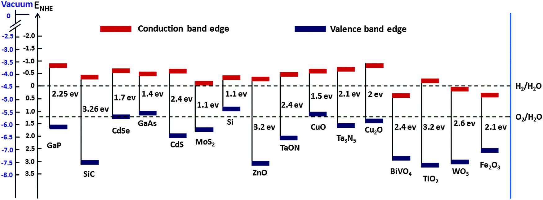 | ||
| Fig. 1 Band edge positions of semiconductors in contact with the aqueous electrolyte at pH = 0 relative to NHE and the vacuum level. For comparison the HER and OER redox potentials are also presented. | ||
As visible-light-driven photoelectrode materials, much attention has been paid to the development of oxides, especially Fe2O3, BiVO4, and WO3, because they are generally inexpensive, stable, and easily prepared on a large scale. Fe2O3 (α is omitted henceforth) based photoelectrodes have been studied most intensively on account of several promising properties. Fe2O3 is earth abundant, non-toxic, photochemically stable with a narrow bandgap (1.9–2.2 eV);29 thus, with an average band gap of 2.1 eV it can achieve a theoretical maximum STH of 15%, which exceeds the STH benchmark efficiency of 10% required for practical applications.30 All these properties make it a potential candidate as a water splitting photoanode for the main proof-of-concept demonstrations. However, several limitations such as a relatively low absorption coefficient (due to an indirect band gap), a very short excited-state lifetime (∼10−12 s), poor oxygen evolution reaction kinetics, a short hole diffusion length, and poor electrical conductivity still hinder the PEC activity of hematite. To overcome these shortcomings various efforts have been made, e.g. nanostructuring, passivating surface localized electron trap states using co-catalysts and thin overlayer coatings, using more than one absorber (heterostructures), using localized surface plasmons, quantum dot sensitization, reduction of film thickness, doping, and introducing electron collecting scaffolds.
3. Scope of the review
This review comprises four main sections, organized as follows: the first part gives details about the electronic structure, the morphology, the photoelectric properties and the photocatalytic reaction mechanisms of hematite. The second part presents a detailed review of the mismatch between the hole diffusion length and light harvesting efficiency in ultrathin hematite nanostructures. Significant emphasis has been given to recent experimental approaches, such as superior light harvesting photonic structures that simultaneously enhance photon absorption and hole diffusion lengths. In the third part great emphasis is paid to the recent emerging strategies employed to improve the water oxidation reaction kinetics that promise to split water at low applied potentials. The outcome of surface passivation layers on charge transfer processes across semiconductor–liquid interfaces will be also discussed in accordance with different approaches. One of the main factors that limit lowering of the practical water oxidation photocurrent (JH2O) is charge separation efficiency (jsep). Therefore, strategies such as doping, the formation of heterojunctions and the application of electron conductive scaffolds to improve the jsep are studied in the fourth part of this review.4. Hematite (α-Fe2O3)
4.1. Magnetic, optical and electronic properties of hematite
In this section we discuss the crystal structure, and magnetic, optical and electronic properties of hematite and band bending in hematite/electrolyte interfaces. In keeping with the theme and motivation of this article, we restrict our discussion to matters relevant to solar energy conversion devices. According to literature reports, polycrystalline n-type iron oxide electrode films were first investigated by Hardee and Bardl using chemical vapor deposition (CVD) onto Ti and Pt substrates.31 Hematite, which is iso-structural with corundum (α-Al2O3),32 is the most thermodynamically stable form of iron oxide under ambient conditions and also the most common form of crystalline iron oxide. The hematite structure has two formula units per unit cell, the trigonal–hexagonal and the primitive rhombohedral unit cells (Fig. 2).33 It contains iron and oxygen atoms arranged in a trigonal–hexagonal unit cell structure with space group R![[3 with combining macron]](https://www.rsc.org/images/entities/char_0033_0304.gif) c and lattice parameters a = b = 0.5034 nm, and c = 1.375 nm, with six formula units per unit cell. For the rhombohedral unit cell, arh = 0.5427 nm and α = 55.3°.
c and lattice parameters a = b = 0.5034 nm, and c = 1.375 nm, with six formula units per unit cell. For the rhombohedral unit cell, arh = 0.5427 nm and α = 55.3°.
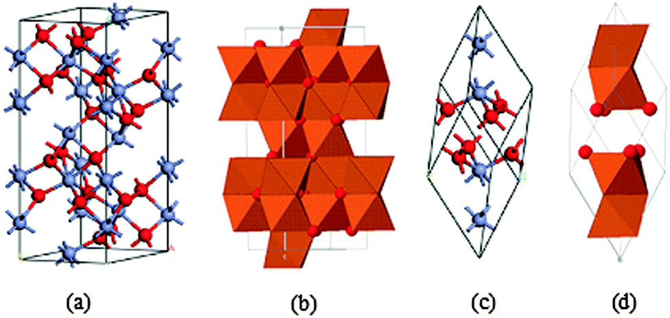 | ||
| Fig. 2 Schematic illustration of the crystal structure of hematite: (a) hexagonal unit cell and (c) rhombohedral primitive cell. The face-sharing octahedra in (a) and (c) are shown in (b) and (d), respectively. The Fe3+ ion is along the c-axis. Color scheme: Fe = grey and O = red. Adapted from J. Phys.: Condens. Matter, 2012, 24, 325504 and Dzade et al., Minerals, 2014, 4, 89–115. | ||
It is easy to understand the hematite structure based on the packing of the anions, O−2, which are arranged in a hexagonal closed-packed lattice (hcp) along the [001] direction with the cations (Fe3+). Two thirds of the sites are filled with Fe3+ ions which are arranged regularly with two filled sites being followed by one vacant site in the (001) plane thereby forming six fold rings.32,34 The arrangement of the cations produces pairs of FeO6 octahedra that share edges with three neighboring octahedra in the same plane with one face in an adjacent plane in the [001] direction (Fig. 2(b)).33 Octahedral face sharing, which occurs along the c-axis, is responsible for the distortion, from ideal packing, of the cation sub-lattice; Fe atoms in the octahedra which share faces are repelled along the direction normal to [001], causing the cations to shift closer to the unshared faces.32,35
Even though the magnetic properties of hematite are not pertinent to its photoelectrochemical performance, the iron spin configuration does influence its optoelectronic and carrier transport properties. These attributes should be properly understood prior to its use as a solar water splitting semiconductor.1 Various studies have shown that the magnetic features of hematite depend on two factors, i.e. temperature1,33,36,37 and particle size.36–38 At room temperature hematite is weakly ferromagnetic, while at above 956 K (Tc) it is paramagnetic. At 263 K it undergoes a magnetic phase transition to an antiferromagnetic state.36–38 This lower temperature transition is called the Morin temperature (TM), below which the two magnetic sub-lattices are oriented along the rhombohedral [111] axis and are exactly antiparallel.37,38 Above TM the magnetic moments lie in the basal (111) plane with a slight canting away from the antiferromagnetic axis resulting in a small net magnetization in the plane.38 Above TM, the Fe3+ ions are antiferromagnetically coupled across the shared faces along the c-axis. The anti-ferromagnetic (AFM) structure is shown in Fig. 3 where iron atoms are coupled ferromagnetically within a single octahedral layer, and alternating layers are coupled anti-parallel along the [0001] direction.39 However, as all iron atoms have an equivalent octahedral environment, the electronic and magnetic properties will be the same at each iron site. A study by M. Chirita et al. observed the strong dependence of the Morin temperature on the size of the particles, generally decreasing with it and tending to disappear below a diameter of ∼8 nm for spherical particles.37 They showed that hematite nanoparticles below 8 nm in diameter have superparamagnetic properties. Another similar study by F. Bødker and coworkers also found that for particles smaller than 8–20 nm, the transition temperature is below 4 K.38 This effect has been explained by a lattice expansion in the small particles, but strain and defects may also be important. In particular, it is known that the spin reorientations in hematite are determined to a large extent by the presence of impurities or substitutions and by the particle's size and morphology.36 Therefore, the magnetic features of hematite are influenced by the method of preparing the sample, which in turn influences the particle size and morphology.
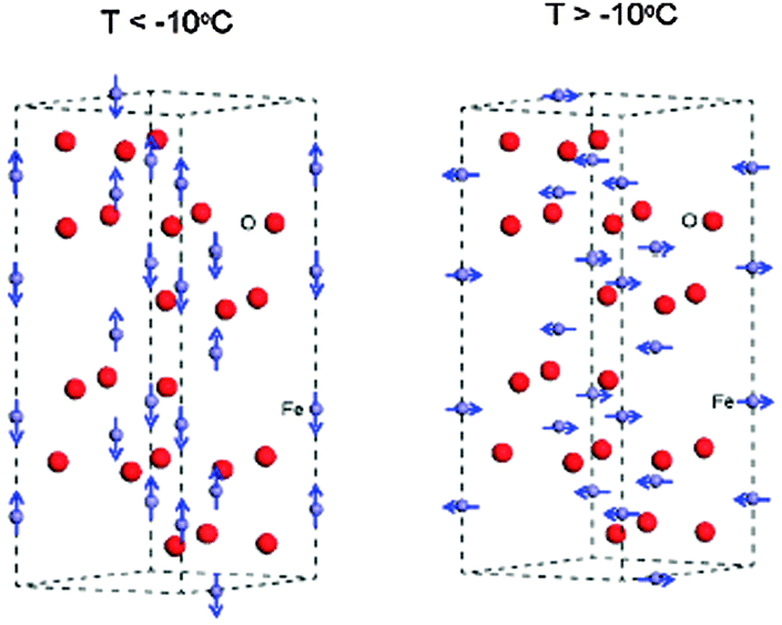 | ||
| Fig. 3 Magnetic order around iron atoms in the hematite hexagonal cell below and above the Morin temperature. Color scheme: Fe = grey and O = red. Adapted from J. Phys. Chem. C, 2013, 117, 3779–3784. | ||
The optoelectronic properties of hematite must be understood to optimize its performance as a solar energy conversion material. The optical absorption bands of hematite begin in the near-infrared spectral region and extend into the UV region.30,40 The optical spectrum of Fe3+ in hematite results from three types of electronic transitions:41,42 (1) ligand field transitions (i.e. d–d transitions), (2) ligand-to-metal charge transfer transitions (LMCT) from the O (2p) non-bonding valence bands to the Fe (3d) ligand field orbitals and (3) pair excitations resulting from the simultaneous excitation of two adjacent Fe3+ cations which occupy adjacent sites.
4.2. Photoelectrochemical water splitting on the hematite photocatalyst
When a semiconductor absorbs photons with energy equal to or greater than its band gap, electrons will be excited from the valence band (VB) to the conduction band (CB), leaving the holes in the VB. Then the electrons and holes migrate to the photoelectrode's surface and are injected into the electrolyte through the co-catalyst to generate hydrogen and oxygen respectively. This electron–hole pair generation process in Fe2O3 can be expressed as follows:| Fe2O3 + hν → (Fe2O3)e− + (Fe2O3)h+ |
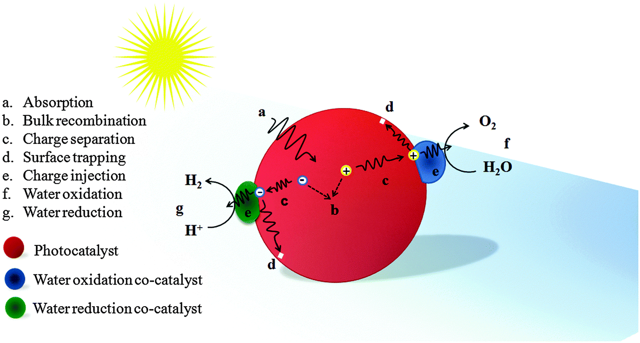 | ||
| Fig. 4 Schematic illustration of an ideal phototocatalyst loaded with water oxidation and reduction co-catalysts with possible photoelectrochemical processes. | ||
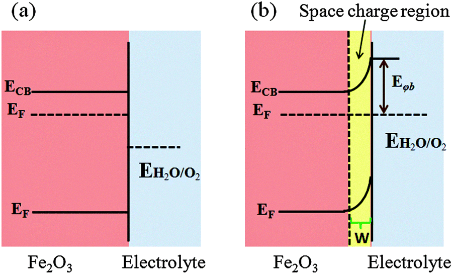 | ||
| Fig. 5 Dark equilibration of hematite (n-type semiconductor) with an electrolyte containing a redox couple potential E. (a) Before equilibration; (b) departure from equilibration. The potential barrier height Φb sets the upper limit to the energy that can be extracted from the junction. | ||
Theoretically, the maximum water oxidation photocurrent (Jmax) for a Fe2O3 photoanode, at a band gap of 2.1 eV under Air-Mass 1.5 Global (AM 1.5G) solar illumination, is 12.5 mA cm−2, which is equivalent to 15.4% STH. However, the practical water oxidation photocurrent (JH2O) is lower due to the limited light absorption (Jabs), charge separation (ηsep), and surface charge injection efficiency (ηinj) of the material, according to JH2O = Jabs × ηsep × ηinj.44,45 Hematite has a light penetration depth of 118 nm at 550 nm which is longer than its hole diffusion length (2–4 nm).46–50 Hence, effective charge generation and separation cannot be achieved in a flat geometry of hematite because increasing the film thickness would lead to more charge carrier accumulation and decreasing the film thickness would lead to less light absorption. The practical consequence is that only holes generated within a few nanometers of the semiconductor liquid junction (SLJ) can reach the interface and be used for water oxidation. The rest recombines with electrons and generates only heat. Charge separation efficiency is limited by both the short hole diffusion length and the very short excited state lifetime (1 ps).51–53 An ultrafast transient absorption measurement showed that the very fast decay of charge carriers in hematite is possibly due to a high density of intrinsic mid-band gap electronic states, internal defect induced trap states, and, to a lesser extent, surface defects.52 Moreover, the poor electrical conductivity of hematite (in the order of 10−2 cm2 V−1 s−1 at room temperature), which is associated with the Fe3+/Fe2+ valence alternation on spatially localized 3d orbitals, also affects the charge separation efficiency greatly. A third limiting factor is the sluggish oxygen evolution reaction (OER) at the electrode/solution interface. This might be due to the rapid capture of holes by the Fe3+ e2g level, which lies above the top of the O 2p6 band, instead of the O 2p6 band itself.54 It has been also shown that surface trap states preferentially trap holes before they reach the electrolyte interface and oxidize water.55 Using transient absorption measurements, Barroso et al. also showed that the existence of interband states can trap holes at the surface.6 Indeed, in the absence of an applied bias, or under a cathodic bias close to flatband potential, these intraband states are largely occupied by electrons and therefore photoholes can rapidly become trapped in these sites. Various strategies have been developed to overcome these limitations. To improve light absorption and photon-to-current conversion efficiency, nanophotophotonic structures, using more than one absorber, with reflective coatings, plasmonic structures, etc., have been employed. Different approaches have been used to enhance the charge separation efficiency such as nanostructuring, doping, using heterojunctions, and incorporating conducting scaffolds. Co-catalysts, surface passivation layers and surface chemical corrosions have been used to facilitate charge injection at the SLJ and reduce the required overpotential.
5. Progress in morphological design
Despite having several advantages, the small carrier harvesting depth of hematite greatly limits its photoelectrochemical performance. Several studies have demonstrated various highly photoactive Fe2O3 morphologies to offset this limitation. In the case of thicker planar Fe2O3 films a majority of photogenerated carriers vanish due to recombination. Therefore, most of the carriers generated far away from the semiconductor–electrolyte interface cannot be collected, resulting in a negligible photocurrent. In addition to this, Souza et al. argued that in thicker films the strong interaction between the film and the substrate induces stress which generates defects in the crystal lattice of the hematite film, increasing the e−–h+ recombination process.56 On the other hand, stacked thin films are considered to be effective approaches to extend the hole transport distance. However, the surface area and photon absorption of this type of photoanode are not high enough.57 A means of resolving this problem is to construct nanostructured electrodes, such as nanoparticles, nanoflowers, nanowires (NWs), nanotubes, or nanocones. For PEC water splitting, the nanostructured materials can offer a large interfacial area between the photocatalyst and the electrolyte, which is favorable for the transportation and separation of charge carriers.58–61 Nanoparticles, dendrites and mesoporous hematite films often suffer from recombination and poor transport across grain boundaries between particles.62 In this regard, one dimensional (1D) nanostructures such as nanowires, nanotubes, and nanorods with high aspect ratios and large surface areas can improve charge carrier collection by minimizing hopping transport and thus reduce recombination losses at grain boundaries.63 Moreover, 1D hematite nanostructures with smaller diameters can minimize the distance needed for the holes to diffuse to the electrolyte–semiconductor interface, thereby avoiding the poor charge transport limitation. Beermann and co-workers recently reported the use of hematite nanorod arrays as photoanodes in a PEC cell and demonstrated that 1D nanostructures could potentially address some of the fundamental PEC issues and increase the device's efficiency.64 Cauliflower nanostructures grown via atmosphere pressure chemical vapor deposition (APCVD) in combination with doping and surface modification with more efficient oxygen evolution catalysts have shown significantly improved performances and made nanostructured hematite a more promising photoanode material. For example Andreas et al. reported cauliflower-like structured hematite with an incident photon current efficiency (IPCE) of 42% at 370 nm at 1.23 VRHE.59 The detailed comparison of nanofilm and 1D nanostructures for water splitting application was reported by Warren's group, in which the better photo-response was obtained by the 1D nanostructured electrode.65 Most recently, an ultrathin hematite photoanode grown on a 3D nanophotonic structure was considered to be an ideal promising morphology.66,67 It has been reported that the 3D nanophotonic structures provided excellent light-trapping capability, ensuring sufficient light absorption with a thin hematite film and a short carrier transport distance. (A detailed account of nanophotonic hematite structures is given in the next section.) Fig. 6 and Table 2 summarize the progress of the morphological evolution of hematite nanostructures for photoelectrochemical water splitting.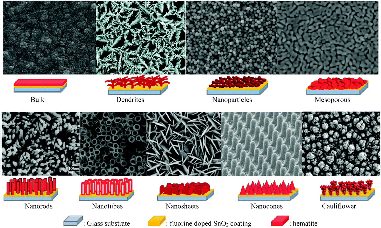 | ||
| Fig. 6 SEM images and representative schemes of different hematite nanostructures grown on the FTO coated glass substrate showing the progress in morphology for photoelectrochemical water splitting. | ||
| Type of nanostructure | Features | Synthesis methods | J at 1.23 V vs. RHE (mA cm−2) | Ref. |
|---|---|---|---|---|
| a The effect of the film thickness has been excluded from samples prepared using anodic electrodeposition. b Under 87 mW cm−2. | ||||
| Bulk | Dense, high e–h recombination, and high photon absorption | Electrodeposition | No photocurrent responsea | Chou et al.68 |
| Dendrites | Dense, poor light absorption, long electron path, and high e–h recombination | Electrodeposition | ∼0.018 | Zheng et al.69 |
| Nanoparticles | More surface area than bulk, long electron path, and low electrode/electrolyte interaction | Anodization | 0.05 | Fu et al.70 |
| Mesoporous | More surface area than bulk and higher electrode/electrolyte interaction than nanoparticles | Colloidal synthesis | 1.1 | Gonçalves et al.71 |
| Nanorods/nanowires | Strong anisotropic conductivity and low grain boundaries | Hydrothermal | 1.24 (Sn doped) | Ling et al.72 |
| Nanosheets | Ultrathin film thickness (<10 nm) and highly dense film (430 nm) | Hydrothermal | 1.4 (Ge doped) | Liu et al.73 |
| Nanotubes | Nanowalls of 5–6 nm thick and high aspect ratio | Sonoelectrochemical anodization | 1.41b | Mohapatra et al.74 |
| Nanocones | Large surface area and enhanced light trapping (absorption) | Template assisted ultrasonic spray pyrolysis | 2.42 (Ti doped) | Qiu et al.66 |
| Cauliflower | High surface area, small feature size crystallites, and porous | APCVD | 2.1 | Zhong et al.75 |
6. The trade-off between absorption and carrier collection efficiency
Many candidate photocatalyst materials suffer from highly reduced charge transport as the minority carrier diffusion lengths are significantly shorter than the absorption depth of light (micrometer scale near the band edge). In this section we will briefly discuss some of the latest advances with respect to the fabrication of ultrathin film hematite photocatalysts giving maximum possible photon absorption. A particular emphasis will be given to light trapping strategies especially nanophotonic structures which are promising solutions to the dilemma of low charge separation and low photon absorption efficiencies. Hematite has a very short hole diffusion length (20 nm,76 2–4 nm49,72) compared to the light penetration depth (α−1 = 118 nm at λ = 550 nm)77 and it results in rapid non-radiative electron–hole recombination inside the semiconductor and thereby greatly limits its PEC performance.78 In general, for an active material with a short carrier diffusion length, thinning down the material can lead to improved carrier collection. However, ultrathin hematite films suffer from low photon absorption due to the mismatch between the photon penetration depth and the film's thickness.Recent studies on thick layers79,80 as well as ultrathin films81 confirm that the efficiency of Fe2O3 photoanodes is mainly limited by the collection of photogenerated holes at the surface. Thus, reducing bulk recombination is the key to improving the internal quantum efficiency (IQE) of Fe2O3 photoanodes, an important step towards efficient, sustainable, durable and potentially inexpensive solar hydrogen production. To start our discussion of ultrathin planar films we begin with a promising approach by Dotan and co-workers.82 They use reflecting coatings and take advantage of resonant light trapping using multiple reflections in a flat hematite film deposited on a reflective surface (Fig. 7(a)). The authors claimed that interference between forward- and backward-propagating waves enhances the light absorption in quarter-wave or, in some cases, deeper sub-wavelength films. This enables maximization of absorption in regions where the photogenerated minority charge carriers (holes) can reach the surface, while minimizing the wasted absorption in regions where they are lost to recombination. Combining this effect with photon re-trapping schemes, such as using V-shaped cells (Fig. 7(b)), provides efficient light harvesting in ultrathin films, overcoming the trade-off between light absorption and charge collection. A water photo-oxidation current density of 4 mA cm−2 was achieved using a V-shaped cell comprising 26 nm-thick Ti-doped Fe2O3 films grown on a substrate coated with a silver–gold alloy back-reflector.82
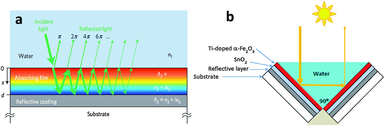 | ||
| Fig. 7 (a) Schematic illustration of the light propagation in a quarter-wave (d = λ/4, for normal incidence) absorbing film on a back-reflector substrate. The different colors represent the light intensity distribution across the film (red, high; blue, low). (b) Schematic illustration of photon re-trapping using a 90° V-shaped cell. Adapted from Nat. Mater., 2013, 12, 158–164. | ||
Even though such ultrathin planar films are advantageous for carrier collection they still suffer from severe light absorption (unless an appropriate light trapping configuration is designed as discussed above) and a low PEC surface area. In this regard 1D nanostructured morphologies with controlled film thickness are beneficial. Besides the smaller feature size and film thickness, the preferential growth orientation of 1D nanostructures also plays a crucial role in improving PEC performance. Iordanova et al. have reported a strong anisotropic conductivity in the hematite lattice, where the conductivity within the (001) basal plane is four times higher than the conductivity along the [001] direction because of a hopping mechanism related to Fe2+/Fe3+ mixed valence states within the iron bilayers.83 Thus arrays of 1D single crystal hematite nanostructures, such as nanoscaled rods, tubes, or wires, attached and oriented vertically to the conducting substrate are important to facilitate the collection of photogenerated electrons, and further enhance PEC efficiency. They provide a direct path that facilitates electron transport, and allows photogenerated holes to efficiently reach the electrolyte interface, while also exposing as many active facets as possible to the electrolyte for water oxidation.
Many studies have demonstrated efficient nanostructured hematite morphologies, while at the same time controlling the size of the nanostructure down to the ultrathin level. The first attempt to synthesize an ultrathin hematite nanostructure was made by Duret and coworkers.84 They synthesized vertically aligned mesoscopic Fe2O3 platelets having a thickness of 5–10 nm and a size of 100 nm using the ultrasonic spray pyrolysis technique. The mesoscopic leaflet structure has the advantage that it allows for efficient harvesting of visible light, while offering at the same time a very short hole diffusion length to reach the electrolyte interface before recombining with electrons. Recently Lui et al. synthesized highly oriented Ge-doped Fe2O3 nanosheet arrays grown in the (001) basal plane and vertically aligned on FTO coated glass substrates using a hydrothermal method (Fig. 8(a)).73 These nanosheets display ultrathin nanostructures with thicknesses of no more than 10 nm and construct a highly dense film with the average overall thickness of 430 nm. Perpendicularly aligned Fe2O3 sheets having a thickness between 15 and 25 nm have also been synthesized by Cesar et al. using ultrasonic spray pyrolysis of their iron precursor solutions. The authors argued that this particular grain size, orientation and morphology (leaf shaped sheets) afford facile transfer of holes to the electrolyte, before the recombination occurs, while still shuttling electrons to the back contact. The addition of silicon produced further improvements in the photo-response that was attributed to morphological changes rather than to electronic effects.58 An innovative work by Mohapatra et al., who synthesized smooth Fe2O3 nanotubes on Fe foil, using a sonoelectrochemical anodization method, targeted the short hole diffusion length of hematite, while simultaneously enhancing photon absorption by controlling the thickness of the nanowalls to 5–6 nm and the overall film thickness to 3–4 μm (Fig. 8(b) and (c)). They found that the charge transport properties of the nanotubes to be 40–50 times higher than those of the nanoparticles, leading to better photoactivity of the nanotubes compared to the nanoparticles.74 Recently, design guidelines for efficient light harvesting nanostructures for applications such as photovoltaics and photodetection were demonstrated using finite difference time domain (FDTD) simulations with Ge as the model material.85 They showed that properly designed nanopillar and nanocone arrays are the most efficient light harvesting morphologies with high broad band solar spectrum absorption capabilities (Fig. 8(d1)–(d4)).
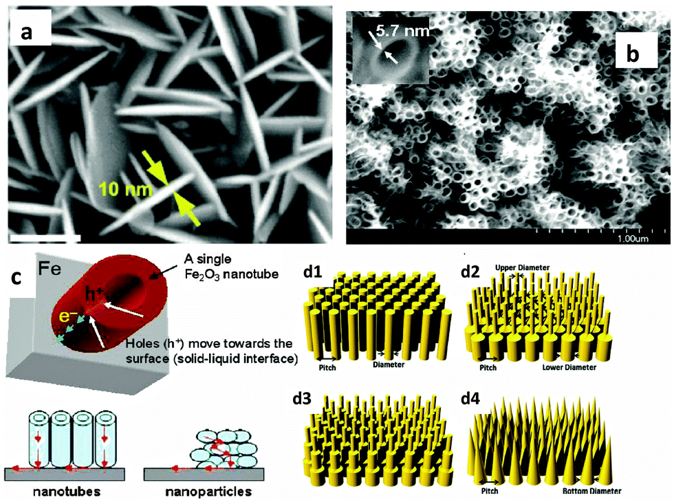 | ||
| Fig. 8 (a) High magnification SEM image of Ge-doped Fe2O3 nanosheet arrays. The scale bar represents 100 nm. Adapted from Nano Energy, 2014, 9, 282–290. (b) High magnification SEM image of vertical Fe2O3 nanotubes oriented on Fe foil. Adapted from Chem. Mater., 2009, 21, 3048–3055. (c) Schematic representation of electron flow towards the back contact (Fe) through the NTs, movement of holes towards the surface, and comparison of the transfer path of electrons through 1D nanotube arrays and nanoparticles to the current collector. (d1) to (d4) represent schematics of hexagonal Ge nanostructure arrays of single-diameter NPL arrays, dual-diameter NPL arrays, multi-diameter NPL arrays and NCN arrays, respectively. Adapted from Nano Energy, 2013, 2, 951–957. | ||
The creation of rationally designed multi-diameter nanopillar or nanocone structured hematite is not as simple as for other monoatomic semiconductors e.g. Si and Ge, due to problems encountered in synthesis. Kim et al. fabricated judiciously nanopatterned multi-walled nanobeam arrays of hematite photocatalysts from lithographically defined Fe nanobeam-arrays and subsequently transformed to iron oxide beams simply by calcination in air at 600 °C for 4–5 min. Such nanostructuring allows sunlight to drive optical resonances that can both enhance the light intensity inside the photoelectrode and favorably redistribute the highest fields to the near surface region from which carriers can effectively be collected without significant recombination.86
An alternative efficient approach that offsets the trade-off between the smaller film thickness and the low photon absorption of hematite is the design and construction of three-dimensional (3D) nanostructures. 3D nanostructured arrays not only enhance carrier collection efficiency (due to shortened diffusion length) but also improve photon harvesting capability at smaller film thickness. Recently, great attention has been given to ultrathin hematite nanocone/nanospike arrays. Their anti-reflective and light trapping properties enable them to absorb the majority of incident light.87
It has been shown using first-principles full-field electromagnetic simulations that near total above-band-gap solar absorption can be achieved in ultra-thin nanocone iron oxide film photoanodes for water splitting applications. Assuming a hole diffusion length of 20 nm, which is within the experimental range, a photocurrent density of 12.5 mA cm−2 can be obtained, which is comparable to the ideal photocurrent limit.88Fig. 9(a) shows a schematic diagram of a 20 nm hematite film on a 3D photonic substrate, where any region of hematite is within the nearest hematite–water interface which is favorable for efficient carrier extraction. Although charge transport is very complex in real hematite electrodes, the authors assumed that all photogenerated carriers in such a design can contribute to the photocurrent. Similar near-unity absorption characteristics are also shown by thinner structures; a simplification that allows us to focus on the optical aspects of such structures. Fig. 9(b) shows the performance of the photonic structures at different total heights (H) relative to the photocurrent (J) generated from single-pass absorption. The authors assumed perfect antireflection at the water–hematite interface for the planar structure with single-pass absorption; however, due to the extremely short hole diffusion length of 20 nm, only the photons absorbed in the first 20 nm region in the hematite can effectively contribute to the photocurrent. On the other hand, in the nanocone structure, all absorption in hematite occurs within 20 nm of the water–hematite interface, and hence all photons can, in principle, contribute, resulting in a much higher photocurrent. In fact, no single material can meet all the requirements of an ideal PEC photoelectrode. Qiu et al. fabricated ultrathin hematite coated on pre-synthesized regular arrays of 3D conductive nanospikes (NSPs).66Fig. 9(c) and (d) show ultrathin hematite film deposited on a 3D nanophotonic Al2O3 structure after deposition of several protective coating layers, including a ∼100 nm thick Ti/Pt metal layer and a ∼200 nm thick FTO layer. It has been stated that the nanophotonic structures can significantly improve light absorption in the ultrathin hematite active material, where the large surface area accommodates the slow surface water oxidation process and act as an efficient carrier collection path. As a result, a high current density of 3.05 mA cm−2 at 1.23 V vs. RHE has been achieved on such nanophotonic structures (Fig. 9(e)), which is about three times higher than that of the planar photoelectrode. Finite-difference-time-domain (FDTD) simulations carried out in the wavelength range of 300 to 600 nm on planar and NSP showed much greater photon absorption on the NSP substrate than on a planar substrate, which shows the light trapping enhancement when the 3D NSP photoelectrode is used. More recently the same research group demonstrated Ti doped hematite with a film thickness of 90–100 nm deposited on a novel 3D hexagonal nanocone array of fluorine-doped tin oxide (FTO) supporting electrodes that showed an 86% increment in current density at 1.23 V vs. RHE compared to its planar counterpart (Fig. 9(f) and (g)).67 The authors claimed that the specially designed 3D FTO layer provides a larger electrode surface area and/or stronger light-trapping compared with the commonly used planar FTO glass substrate. To fully utilize the special light harvesting property of the 3D FTO structure, a gold layer was deposited under the Fe2O3 film to concentrate the incident light into the near surface region. Finite different-time-domain (FDTD) simulations have also been performed to confirm the strong light trapping property of the 3D FTO substrate and the surface light absorption enhancement brought about by the gold layer (Fig. 9(h)). The authors argued that as the distance between neighboring cones is close to the incident light wavelength, the incident light becomes diffracted and the electromagnetic wave will re-distribute in the nanocone area, leading to a significant electric field enhancement around the 3D structure. In other words, the incident light has been “trapped”. In addition to this, the electric field at the surface of the Fe2O3 layer has been significantly enhanced in the 3D structure, resulting in more efficient absorption by the active material.
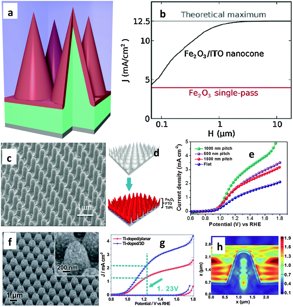 | ||
| Fig. 9 (a) Core–shell nanocone arrays with a three-dimensional view of the right circular cones forming a square lattice on the substrate. (b) Photocurrent generated by the structure with a range of nanocone heights, compared to the single-pass photocurrent. Adapted from ACS Photonics, 2014, 1, 235–240. (c) Sixty degree tilted SEM view of Fe2O3 decorated nanospikes (NSPs). (d) Schematic diagram of multiple layer thin film deposition including Ti/Pt of 100 nm, FTO of 200 nm and Fe2O3 of 85 nm for water splitting device fabrication. (e) J–V curves of the Ti-doped hematite photoelectrodes based on the three different NSP arrays, showing the best performance achieved with the 3D NSP array photoelectrode with a pitch of 1000 nm. Adapted from Nano Lett., 2014, 14, 2123–2129. (f) SEM image of undoped Fe2O3 on the 3D FTO substrate, 45°-tilted view. The inset shows one of the Fe2O3-coated FTO nanocones in detail. (g) J–V curves of Ti-doped Fe2O3 on planar FTO (red curve) and 3D FTO electrodes (blue curve). (h) FDTD simulation results of the 3D electrodes with a gold reflection layer at a wavelength of 500 nm, respectively. Adapted from Energy Environ. Sci., 2014, 7, 3651–3658. | ||
The recent and rapid development of surface plasmon resonance (SPR) combined with thin films has also offered a new opportunity to overcome the limited efficiency of hematite photoanodes.89–92 SPR improves the solar-energy-conversion efficiency by (i) extending light absorption to longer wave lengths, (ii) increasing light scattering, and (iii) exciting electron–hole pairs in the semiconductor by transferring the plasmonic energy from the metal to the semiconductor.93 In 2011, Gao et al. published a report on the synthesis of ultrathin hematite nanopilars patterned on pre-synthesized Au nanopillars92 (Fig. 10(a)). The gold nanopillars were first fabricated by nanoimprinting. Then they deposited the photoanode material (Fe2O3) on the Au surface using electron-beam-evaporated metallic Fe followed by annealing in pure oxygen at 450 °C for about 1 hour. It was stated that the enhanced saturated photocurrent density of the iron oxide thin-film photoanode coated on arrays of Au nanopillars (Fig. 10(b)) was attributed primarily to the increased optical absorption originating from both SPR and photonic-mode light trapping in the nanostructured topography. The resonances can also be tuned to a desirable wavelength by varying the thickness of the iron oxide layer. A similar approach was reported by Li and co-workers on the use of photonic and plasmonic energy-transfer enhancement techniques to enhance the PEC performance of hematite.89 They reported a unique heterostructure which consists of a hematite nanorod array grown on a plasmonic gold nanohole array pattern (Fig. 10(c)). As the nanohole array is filled with the hematite nanorods, the extraordinary optical transmission launches a guided wave mode inside the nanorod similar to an ‘optical fibre’, creating the confined modes, which trapped the incident light and enhanced the light absorption further. The authors argued that this heterostructure not only reduces the charge recombination rate but also enables both photonic and plasmonic energy-transfer enhancement in a wide ultraviolet-near-infrared spectral region. Using this configuration, a tenfold enhancement in photocurrent density was achieved at 0.23 V vs. Ag/AgCl (Fig. 10(d)) by taking the whole geometric area of the photoanode instead of the effective electro-active area.
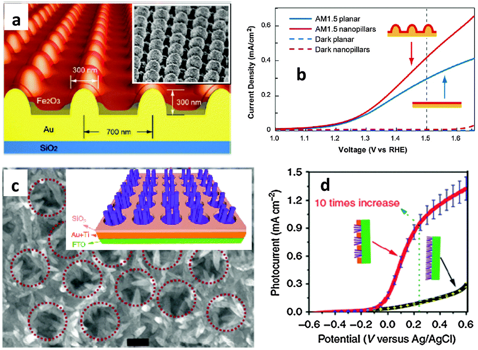 | ||
| Fig. 10 (a) Schematic illustration of Au nanopillars having 300 nm in diameter at the base and 300 nm in height. Connected by a 200 nm thick planar Au film, the nanopillars were patterned in square arrays with 700 nm pitch. Inset: SEM image of 30° tilted of 90 nm Fe2O3 coated Au nanopillar arrays and (b) the J–V curves show the enhancement of the photocurrent from the patterned Fe2O3 electrode as compared to the planar control under AM 1.5 simulated solar illumination. (c) Scanning electron microscopy images of the Au nanohole array with the hematite nanorods with a scale bar of 200 nm. The inset shows the scheme for the growth of the hematite nanorod array on the Au nanohole array. (d) J–V curves under the illumination of AM 1.5G full-spectrum solar light with a power density of 100 mW cm−2. Adapted from, Nat. Commun., 2013, 4 and ACS Nano, 2011, 6, 234–240. | ||
7. Enhancing water oxidation kinetics
The poor oxygen evolution reaction kinetics of the hematite electrode is one of the major challenges that limits its solar conversion efficiency and thereby imposes the requirement of a large applied potential to drive water oxidation. This is due to insufficient transfer of photogenerated holes from the electrode's surface to the electrolyte solution (hole injection) which occurs only under high applied potentials. This is typically attributed to the large amount of recombination between electrons in the conduction band and oxidized surface states at low applied potentials.50,94,95 Even though the nature and role of these surface states remain a topic of debate, as highlighted in several recent perspectives, all of them showed that surface states greatly affect the intrinsic onset potential of hematite.50,94–96 To date, the preparation of hematite with intrinsically low onset potential has remained a great challenge. Various studies reported that the intrinsic onset potential of hematite ranges between 0.7 and 1.1 V vs. RHE in 1 M NaOH electrolyte.97–100 In August 2014 Han et al. published a communication article reporting on the preparation of a unique gradient structure photoanode directly oxidizing Fe foil in a H2/O2 flame at ca. 1700 K that shows the lowest intrinsic onset potential of 0.58 V vs. RHE for the PEC water oxidation. This extremely low onset potential observed is mainly ascribed to the passivation of surface trap states by high temperature heating treatment and the facile charge migration facilitated by the gradient structure of the photoanode.101 The higher overpotential of hematite can be improved either by lowering potential-dependent rate constants for surface-mediated charge recombination or by increasing the rate constant for hole transfer from the photo-electrode to the molecular reactant.102 The former can be accomplished by passivating surface localized electron trap states, e.g. by deposition of surface trapping overlayers and chemical treatment techniques.60,99,103 The latter can be overcome by deposition of oxygen evolution reaction (OER) catalysts. In this section we will focus on recent strategies employed to lower the overpotential of hematite for PEC water oxidation.7.1. Cocatalyst
One of the biggest challenges in water splitting is to overcome the thermodynamically ‘uphill’ hydrogen and oxygen evolution half reactions which involve four-electron transfer reactions.104 Cocatalysts loaded on the surface of semiconductors have been proven to be able to facilitate photocatalytic reactions by accommodating excited electrons/holes and promoting redox reaction kinetics. They facilitate water oxidation reactions usually through the oxidation of the metallic element of the co-catalyst itself which assists hole transport from the hematite surface to the electrolyte. For example the electrochemical, XANES, and EPR analyses have indicated that the electrocatalytic function of the famous cocatalyst, Co–Pi, is associated with oxidation from Co(II) to Co(III) and Co(IV), leading to the formation of high-valence Co(IV)–O intermediates.105–107Fig. 11 schematically describes the role that cocatalysts play in photocatalytic and PEC water oxidation. Overpotential is always necessary to drive the water oxidation reaction due to the activation energy barrier. The presence of cocatalysts on photoanodes can improve the photocurrent and negatively shift the overpotential (Fig. 11(a)) by decreasing the activation energy (Fig. 11(b)) and improving the solar and electric energy utilization efficiency.98,104 The negative shift of onset potential corresponds to the lowering of the overpotential.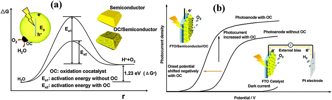 | ||
| Fig. 11 Schematic description of the role of oxidation cocatalysts in (a) photocatalytic and (b) photoelectrochemical water splitting systems. Adapted from Acc. Chem. Res., 2013, 46(8), 1900–1909. | ||
Noble metal oxides such as IrOx108,109 and RuOx110 have been investigated as conventional water oxidation cocatalysts. It has been reported that the surface modification of nanostructured hematite photoanodes by IrO2 nanoparticles (ca. 2 nm diameter) resulted in a 200 mV shift in the photocurrent onset potential and an increase in the plateau photocurrent from 3.45 to 3.75 mA cm−2vs. VRHE under standard testing conditions.109 A stoichiometric IrOx, with x ≈ 2.1, also showed a 300 mV cathodic shift in photocurrent onset potential with the highest surface concentrations of IrOx tested.108 Even though iridium oxide is one of the best water oxidation catalysts, iridium is an expensive non-abundant element. In this context, recent developments have been made in earth abundant Co and Ni based catalysts which could achieve the target of a high turnover frequency (TOF) and are stable inorganic based oxide catalysts which could be used on a large scale. Cobalt-based cocatalysts e.g. cobalt oxide,111 cobalt hydroxides112 and cobalt phosphate75,106,113–116 have been investigated for PEC water oxidation on hematite. Zhong et al. demonstrated the deposition of the Co2+ cocatalyst on the hematite photoanode using different approaches, photo-assisted electrodeposition of Co–Pi, electrodeposition of Co–Pi, and Co2+ wet impregnation (Fig. 12(a)–(c)).75 The authors argued that by allowing deposition only where visible light generates oxidizing equivalents, photo-assisted electrodeposition provides a more uniform distribution of Co–Pi onto Fe2O3 than that is obtained by electrodeposition. A stable −170 mV cathodic shift was observed with photo-assisted electrodeposition of Co–Pi, while electrodeposition of Co–Pi and Co2+ impregnation gave cathodic shifts of 100 mV and 80 mV, respectively. Very recently, Han et al. reported PEC water oxidation on a hematite photoanode at low applied potential.101 First, they lowered the intrinsic onset potential of a hematite photoanode to 0.58 V vs. RHE by the passivation of surface states using H2–O2 flame treatment at a high temperature to suppress surface charge recombination. Then, the onset potential further shifted to 0.50 V after the Co–Pi cocatalyst has been deposited. These impressive results represent the most favorable photocurrent onset potential reported to date for a hematite-based photoanode. It has also been reported that in spite of some additional light absorption losses,115 the Co–Pi cocatalyst can cause a pronounced cathodic shift in the onset potential of Fe2O3 photoanodes.48,105–107,115 In some reports, the decrease in onset potential was accompanied by increased saturated photocurrent densities. For instance, Kim et al. showed that modifying Pt doped Fe2O3 photoanodes with the Co–Pi cocatalyst increases the generated photocurrent by 170% to 4.32 mA cm−2, which is the highest stable PEC water oxidation current for the hematite photoanode reported.48 Other efficient Co-based cocatalysts are Co3O4 and Co(OH)2. Previously an hematite photoanode has been coated with an ultrathin cobalt oxide layer by atomic layer deposition (ALD).100 1 ALD cycle, depositing <1 monolayer of Co(OH)2/Co3O4, resulted in a 100 to 200 mV cathodic shift in the photocurrent onset potential. Furthermore, the optical transparency of the ultrathin Co(OH)2/Co3O4 coating establishes it as a particularly advantageous treatment for nanostructured water oxidation photoanodes. In a similar report, a 40 mV cathodic shift of water oxidation overpotential with hematite nanorods has been observed upon decoration with Co3O4 nanoparticles.111 Although the advantages of coupling cobalt-based species with hematite photoanodes have been widely confirmed, it has to be born in mind that the reasons remain unclear. The controversy centers mainly on whether the photogenerated holes are transferred to and stored by the cobalt oxide layer, or the enhancement is largely due to the formation of a heterojunction between the photoanode and the Co overlayer which contributes to enhance electron depletion in Fe2O3. In the latter case CoOx is playing a noncatalytic role.113,114,117,118
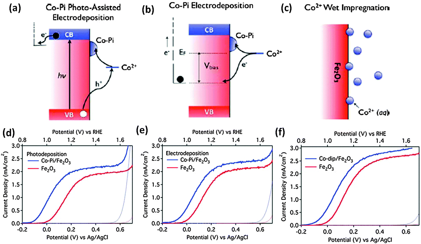 | ||
| Fig. 12 (a–c) Schematic illustration of different Co deposition approaches. Dark-current (dotted) and photocurrent (solid) densities of (d) a Co–Pi/Fe2O3 electrode prepared by photo-assisted electrodeposition, (e) a Co–Pi/Fe2O3 electrode prepared by electrodeposition, and (f) a Co2+/Fe2O3 electrode prepared by surface adsorption (all in blue), compared to the parent Fe2O3 photoanodes (all in red). Adapted from Energy Environ. Sci., 2011, 4, 1759–1764. | ||
Recently, Ni based OER catalysts such as nickel hydroxide,47,119 nickel oxide119 and nickel borate120–122 have attracted a lot of interest, due to their efficient catalytic performance, low cost and low toxicity. Ni–Bi OEC discovered soon after the development of the Co–Pi OEC showed promising oxygen evolution properties under mild conditions similar to that of a Co–Pi OEC.120 Hong et al. showed that photodeposition of a Ni–Bi OEC on hematite nanorods led to a >200 mV cathodic shift in the onset potential for water oxidation and a 9.5 fold enhancement in the photocurrent density at 0.86 V vs. RHE compared to the parent hematite photoanode.122 Recently our group has also demonstrated a NiOOH modified codoped (Sn,Zr) α-Fe2O3 photoanode with a significantly lower onset potential (0.58 V, Fig. 13(a) and (b)). Interestingly, in contrast to an unmodified codoped photoanode, a 160 mV cathodic shift in the photocurrent onset potential and a 1.6 to 9.5 fold enhancement in the charge injection efficiency (ηinj) in the kinetic control region, i.e. 0.7 to 0.9 V, were also observed. We employed a photo-assisted electrodeposition technique which helps to deposit a more uniform and compact NiOOH layer with the optimal loading amount. Ni(OH)2 has also been reported as an efficient water oxidation catalyst on hematite electrodes. Kelley and co-workers used atomic layer deposition to deposit NiO onto thin-film Fe2O3 electrodes for photocatalytic water splitting.119 The authors claimed that photoelectrochemical conditioning of the deposited NiO converts it to Ni(OH)2, which results in a stable reduction of the photocurrent onset potential for water oxidation by −300 mV and improves photocurrent density by two-fold at 1.23 V vs. RHE as compared to untreated Fe2O3. It has been proposed that the catalytic mechanism of the Ni(II) catalyst for water oxidation is a two-step process that involves the fast initial oxidation of Ni2+ to Ni3+, followed by the slow oxidation of Ni3+ to Ni4+, which is believed to be the active catalytic species for water oxidation.47 The catalytic action of Ni(OH)2 on the hematite photoelectrode is thought to result from the suppression of the photoinduced charging effect.47
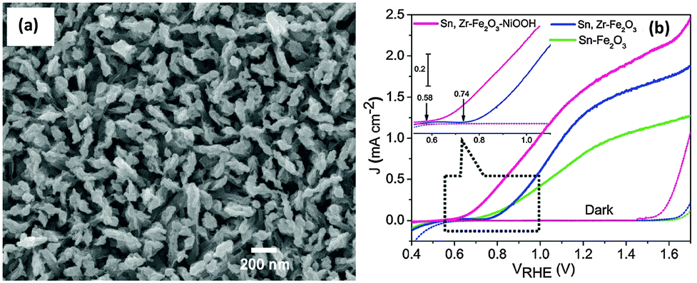 | ||
| Fig. 13 (a) SEM image of codoped (Sn,Zr) Fe2O3 modified with photodeposited NiOOH. (b) Photocurrent density as a function of applied potential in dark and illumination. Adapted from J. Mater. Chem. A, 2015, 3, 5949–5961. | ||
7.2. Surface passivation layers
Photogenerated holes that successfully navigate through the bulk of the hematite electrode and reach the electrode/electrolyte interface are still susceptible to loss by recombination with photoelectrons at surface sites (Fig. 14(a)).50,55,60,123,124 It has been found that the hole-transfer step leading to water oxidation takes place predominantly from surface trapped holes, and not directly from valence band holes. Therefore the photocurrent onset appears only after holes start to accumulate in these surface sites.50 As highlighted in several recent perspectives, the nature and role of surface states remain a topic of debate.55,125 For example, it has been suggested that the surface states are iron-based intermediates that are directly involved in the water oxidation mechanism.95,125,126 In contrast to this, Le Formal et al. have portrayed surface states as more of an electronic state.127 In this case, the surface states are not chemically involved in water oxidation; rather, they are only a source of deleterious recombination.103 Bard et al. mentioned that these electronic states on the surface of an oxide photoanode, due to oxygen vacancies or crystal defects, could cause a degree of the so-called Fermi level pining.128 The sluggish hole transfer (injection) from the electrode to electrolyte interface can be improved by employing co-catalysts (Fig. 14(b)) or non-catalytic passivation layers (Fig. 14(c)). These two phenomena have fundamentally different mechanisms in assisting hole transport. Surface passivation (a non-catalytic process) implies the reduction of hematite surface defects which reduces the hole–electron recombination rate, while a co-catalyst usually implies the oxidation of the metallic element of the co-catalyst which assists hole transport from the hematite surface to the electrolyte.123 In this section, passivation layers which have been recently formed on Fe2O3 that effectively accelerate solar water oxidation by passivating surface states will be reviewed.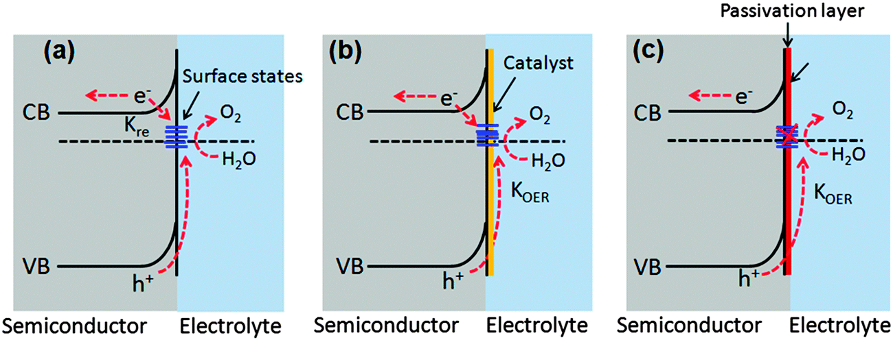 | ||
| Fig. 14 Comparison of the band structure of an n-type semiconductor photoanode in the presence and the absence of passivation layers inside a PEC cell. (a) High charge recombination at surface defects and inefficient water oxidation by the photogenerated holes. (b) Use of an OER catalyst layer, which promotes facile hole transfer across the interface to the electrolyte for improving water oxidation; (c) use of thin non-catalytic passivation layers which suppress surface recombination and improve water oxidation. | ||
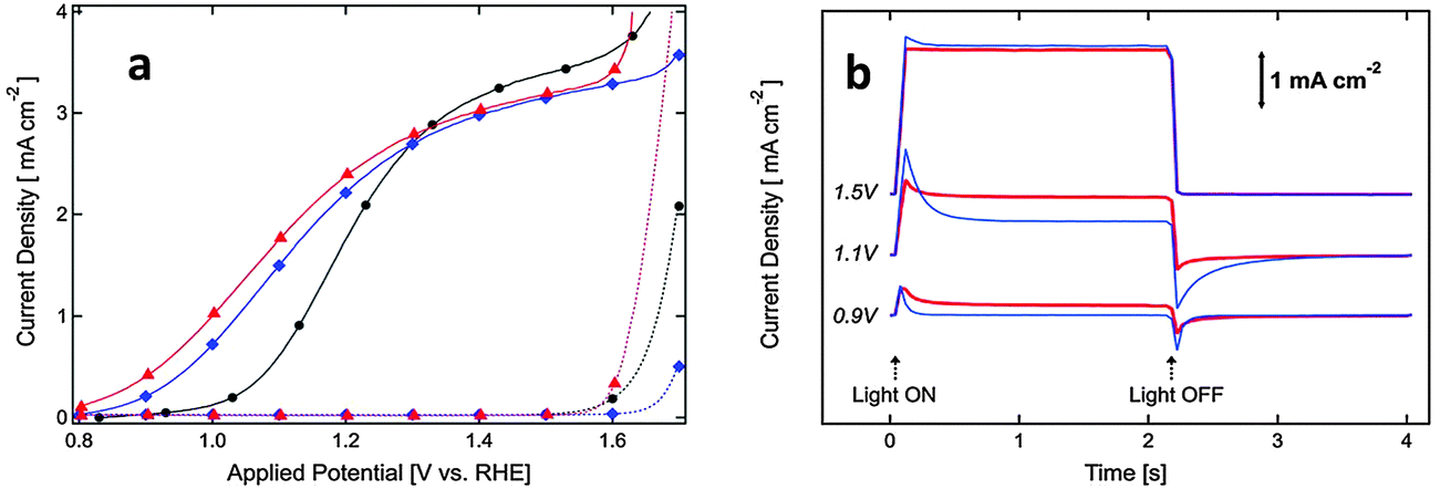
Several noncatalytic oxide layers on hematite have also been shown to affect surface OER behavior, even though no catalytic sites exist to enhance the charge transfer process. Hisatomi et al. deposited 13-group oxides such as Al2O3, Ga2O3, or In2O3 on ultrathin hematite film (27–30 nm thick) photoanodes using a chemical bath deposition technique, which led to 70, 250 and 150 mV cathodic shifts in onset potential compared to the bare hematite, respectively. It has been proposed that the corundum-type overlayers released the lattice strain of the ultrathin hematite layer and decreased the density of surface states.129 Similarly, Le Formal and co-workers have found that an ultra-thin coating of Al2O3 deposited on the state-of-the-art nanostructured Fe2O3 photoanode reduces the overpotential as much as 100 mV and increases the photocurrent by a factor of 3.5 at +1.0 V vs. RHE under standard illumination conditions (Fig. 15(a)). More importantly, this effect was distinguished from a catalytic effect by the subsequent addition of Co2+ ions as a catalyst. The cobalt treatment further decreases the overpotential, suggesting that surface passivation strategies can be combined with catalytic approaches.60 They have also found that after one ALD cycle the photocurrent onset was dramatically shifted cathodically and resistive behavior characterized by a slow and linear increase of the photocurrent with applied voltage was observed. This behavior is possibly due to a high degree of disorder in the amorphous Al2O3 overlayer that inhibits hole injection from Fe2O3 into the electrolyte. After annealing in air at 300 °C the electrode's photocurrent curve regained a shape similar to that before the ALD. It was also apparent from transient photocurrent measurements that photoanodes with 3 ALD cycles of the Al2O3 overlayer showed enhanced charge injection efficiencies at three different potentials (evidenced from anodic and cathodic current spikes) (Fig. 15(b)). However this approach is limited by the photoelectrochemical dissolution of the Al2O3 layer after long term exposure in 1 M NaOH (ca. 1 h) under an applied potential of 1.03 V vs. RHE and 1 sun illumination.60
 | ||
| Fig. 15 (a) J–V curves in the dark (broken lines) and under simulated solar illumination (AM 1.5G, 100 mW cm−2, solid curves). (a) Black circles represent the hematite photoanode before ALD treatment, blue diamonds represent it after 3 ALD cycles of alumina and annealing to 400 °C and red triangles represent it after subsequent cobalt treatment. (b) Transient photo-response is shown by light chopping current densities as a function of time. The red line and blue lines represent the comparison of the transient behavior of iron oxide photoanodes with and without 3 ALD cycles of the Al2O3 overlayer. Adapted from Chem. Sci., 2011, 2, 737–743. | ||
Recently, Yang et al. reported that treatment of the hematite surface by ultrathin TiO2 using atomic layer deposition (ALD) showed a 100 mV cathodic shift from the ‘turn on’ potential.130 Previously Le Formal et al. studied ALD-grown TiO2 as a surface passivation layer but did not report a cathodic shift from the turn-on voltages.60 The difference is suspected to be from the difference in growth conditions as well as from the post growth annealing temperatures.130 Ti-doped Fe2O3 with Al3+ treatment has also been reported by Fu et al. to passivate the surface states, which displayed a 100 mV cathodic shift from the onset potential and a notable improvement in the photocurrent density.131 This cathodic shift from the onset potential is comparable with the values obtained by using an Al2O3 surface passivating over-layer.60 Interestingly, the photocurrent density increased about 10 times at 1.23 V vs. RHE. It has been found that a passivating over-layer of Al2O3 decreases the photocurrent density at high potentials, while surface treatment with Al3+ increases the photocurrent density at high potentials. The results suggest that enhancement in photocurrent density and shift in onset potential are not caused by accelerated OER kinetics.131 Xi et al. also demonstrated a very thin ZnO overlayer from a solution of ZnAc on top of a thin film of hematite and found an increase in the photocurrent and a reduced onset potential.132 After 3 cycles of ZnAc treatment, the photocurrent increased more than 40% to 1.08 mA cm−2 at 0.23 V vs. Ag/AgCl with a −170 mV shift in onset potential. It has been proposed that the ZnO overlayer changes the flat band potential of hematite, which is likely to be the result of electron donation from ZnO to the Fe2O3 interface, and reduces the surface defects. This thin layer of ZnO may also act as an electron blocking layer to prevent electrons leaking from hematite into the electrolyte.132
Surface doping with metal ions has also been proven to be an alternative way to achieve an enhanced PEC performance from α-Fe2O3 photoanodes by promoting charge migration and/or creating a doped overlayer to catalyze the surface water oxidation reaction. For example Xi et al. reported that the current improvement in Fe2O3 nanorod arrays treated by surface Sn doping was mainly attributed to a reduced electron–hole recombination at the hematite–electrolyte interface through the formation of a FexSn1−xO4 layer.124 This has been achieved by treating hydrothermally grown iron oxyhydroxide (FeOOH) nanorod arrays with Sn(IV) aqueous solution before subsequently annealing at 750 °C in air for 30 min. During annealing, the solvent was evaporated and a very thin layer of SnO2 was formed coating the hematite nanorods. Following a solid-state diffusion reaction, Sn(IV) is gradually incorporated into hematite forming an FexSn1−xO4 layer. The presence of this layer is thought to passivate surface defects as well as suppress the tunneling of electrons from the hematite core.124 Similar to this approach, an α-Fe2O3 nanotube photoanode with a thin NixFe2−xO3 overlayer on the surface showed a ∼280% enhancement of the photoconversion efficiency relative to the pristine α-Fe2O3 nanotube photoanode.133 This enhancement was induced by the NixFe2−xO3 overlayer and was attributed to the promoted charge migration, accelerated surface oxygen evolution, and inhibition of low-energy photoexcited hole recombination at the semiconductor–liquid junction. Remarkably, the onset potential of photocurrent of the Ni-doped sample was also cathodically shifted by ∼100 mV, and the slope of photocurrent of the Ni-doped sample was 2–3 times greater than that of the pristine sample (Fig. 16). To illuminate the surface acceleration action of NixFe2−xO3, the authors used a Ni-based catalyst on the surface of a pristine sample as a reference sample. They found lower electron–hole recombination which was claimed to be due to the passivated surface trap states by the NixFe2−xO3 layer as well as by the accelerated OER process, considering the amount of trap states of Fe2+ presented on the surface of pure hematite. The possible mechanism of the NixFe2−xO3 overlayer followed by catalyst deposition, catalyzing the water oxidation reaction could be proposed in Fig. 16. Recently, an AgxFe2−xO3 passivating layer with a thickness of 2–3 nm has also been demonstrated on Ag-doped Fe2O3 nanorod films. It has been reported that this ultrathin layer not only increased the carrier density in the near-surface region but also accelerated the surface oxidation reaction kinetics, synergistically contributing to the improved photoelectrochemical performances.134
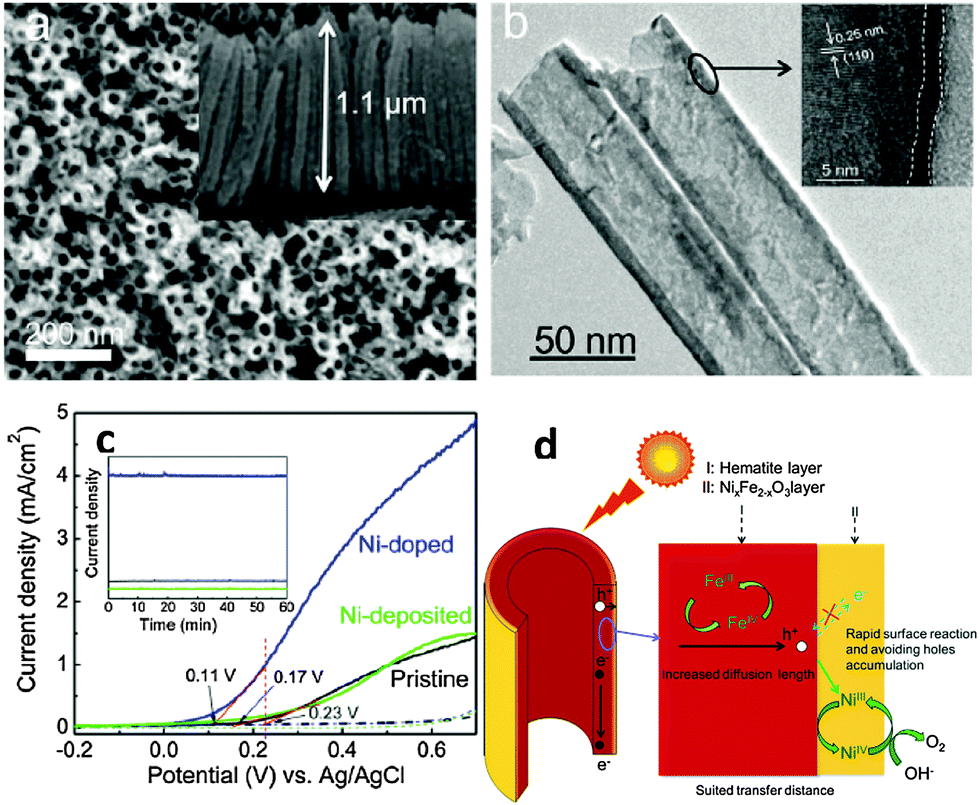 | ||
| Fig. 16 (a) Top-view FESEM image of the Ni-deposited sample and the inset shows the cross-sectional image of hematite nanotube arrays. (b) TEM image of the Ni-doped sample and the insets show the HRTEM image for the marked area. (c) Current density (the inset plot is photochemical stability curves). (d) Schematic diagram of the possible OER process. Adapted from J. Phys. Chem. C, 2012, 116, 24060–24067. | ||
It has been suggested that it is possible to address the problems of surface trap recombination and sluggish reaction kinetics independently by employing surface passivation layers and catalysts sequentially.55 However, convincing evidence that a surface treatment can perform as a true catalyst is still elusive. Rather, it seems more likely that catalysts can act to passivate surface states if they are present or, in the case of already-passivated electrodes, decrease electron–hole recombination by increasing band bending.
7.3. Surface chemical corrosion
Surface corrosion can improve photocatalytic oxygen evolution reaction by changing the chemical state of the electrode's surface. In some semiconductor photoelectrodes, such as Si,135,136 ZnO,137 Cu2O,138,139 and some binary or ternary metal sulfides, surface corrosion has dual benefits – interfacial charge transfer assistance and surface recombination inhibitors. However, hematite is kinetically stable under oxidizing conditions, hence surface corrosion helps to passivate surface states and thereby oxidize water at low applied potentials.123 Recently, Li et al. reported hydrogen-treated hematite nanostructures which have been prepared by a simple pyrolysis of NaBH4 in a crucible.99 The hydrogen treated photoanode showed over 2.5 times higher photocurrent density and 120 mV cathodic shift in the onset potential than that for pristine hematite. The significant improvement of the photocurrent was claimed to be attributed to increased oxygen vacancies after the H2 treatment while the cathodic shift of the onset potential was attributed to the surface effect of H2 treatment. The authors used X-ray absorption spectroscopy to examine the oxygen vacancy and they found that the oxygen vacancy mainly affects the bulk properties but has no contribution to the onset potential. They suggested two possible reasons for the decrease in onset potential. First, the optimized oxygen vacancy content in the surface may lower the onset potential by improving the conductivity of hematite thereby reducing the recombination of photoexcited holes with electrons. Second, reaction of H2 at the electrode surface may result in surface corrosion by taking oxygen atoms away from the hematite. It has been reported that the presence of surface defect states of Fe2+ in hematite is the reason for high onset potential. However, the XAS results in this report indicated that after the H2 treatment, Fe2+ exists on the surface of hematite with oxygen vacancies. Surface-sensitive soft X-ray absorption spectroscopy also confirmed the electronic structure change of the surface of H2-treated hematite. The XAS results clearly confirm that the oxygen vacancies only exist on the surface of the H2-treated hematite samples, suggesting that the onset potential shift between H2-treated hematite and oxygen-deficiency treated hematite should be attributed to the surface effect by the H2 treatment. As we mentioned earlier, a hematite photoanode with the lowest intrinsic onset potential (0.58 V vs. RHE) was recently prepared by heating iron foil in a H2–O2 flame at ca. 1700 K for 10 s.101 It has been stated that due to the slow diffusion of oxygen from the surface to the bulk during the H2–O2 flame treatment a gradient structure composed of the hematite outer layer followed by Fe3O4 and FeO interlayers has been formed. The extremely low onset potential observed is mainly ascribed to the passivation of surface trap states by high temperature heat treatment and the facile charge migration facilitated by the gradient structure of the photoanode. Moreover, by further depositing a Co–Pi catalyst, they obtained the lowest ever reported onset potential of the hematite photoanode (0.50 V vs. RHE). In August 2013, Cao et al. published a report on surface corrosion of Ti4+ doped Fe2O3 with an HCl acid solution which showed 100 mV cathodic shift in the photocurrent onset potential (Fig. 17(a)).140 Unlike other reports, the authors argue that the cathodic shift of the onset potential was not from accelerating water oxidation kinetics, passivating surface states or ion adsorption rather it was due to suppressing the back reaction of electrons. From the dark current results (Fig. 16(b)), the onset potential shifted anodically after surface corrosion, which is contrary to the cathodic shift of the photocurrent onset potential, suggesting that accelerating water oxidation kinetics is not the reason for the onset potential shift. To examine the surface atomic composition before and after corrosion they used XPS and ICP analysis. The XPS and ICP results suggested that there was obvious TiO2 segregation which possibly formed a Fe2O3–TiO2 solid solution on the Ti4+ doped hematite surface. After the surface treatment, the Ti-rich layer was partly removed. Therefore, the surface corrosion effect on the onset potential shift mainly comes from the Fe3+ dissolution and not from Ti4+ dissolution. The cathodic shift of the onset potential is observed both on pure and doped Fe2O3 samples. Therefore, it has been argued that the surface corrosion effect on the onset potential shift mainly comes from Fe3+ dissolution and not from Ti4+ dissolution. Previously the same group used a similar surface corrosion method to improve the performance of a Mo doped BiVO4 photoanode.141 In that work, they found that the surface pretreatment only had an effect on a Mo doped BiVO4, but not on the pure samples. In that case, removing MoOx segregation on the surface, which played a role as a recombination center, was considered to be the main reason.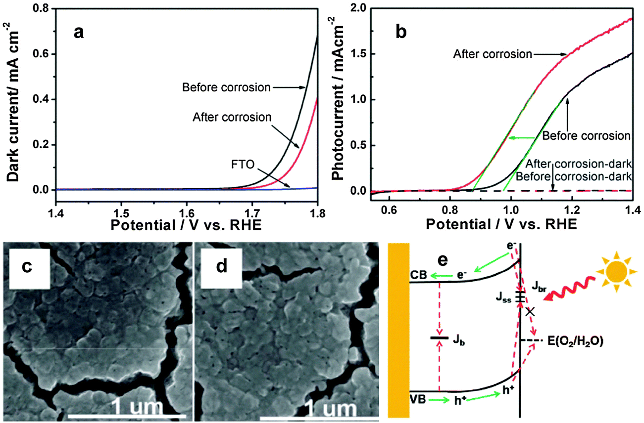 | ||
| Fig. 17 (a) Dark current for water oxidation on the Ti4+ doped Fe2O3 electrode before and after surface corrosion, with the FTO substrate as the reference electrolyte. (b) Photocurrent vs. potential curves of the Ti4+ doped sample before and after surface corrosion, in the 1 M NaOH electrolyte. (c and d) SEM images of the Ti4+ doped sample before and surface corrosion show no obvious change of the surface morphology. (e) A mechanism for the cathodic shift of the onset potential on a Fe2O3 photoanode after surface corrosion. Adapted from J. Phys. Chem. C, 2012, 116, 5076–5081. | ||
Related to the surface corrosion of hematite electrodes, Hu et al. showed bias-free water reduction using a surface modified (CoF3 aqueous solution) Ti-doped iron oxide photoelectrode.142 It was stated that the adsorption of fluoride on the electrode's surface shifts the conduction band to a potential more negative than the redox level of H2/H+, allowing the photogenerated electrons to directly reduce water to H2. A further increase in the photocurrent was observed when glucose was used as the electron donor (rather than hydroxyls) in the electrolyte, helping to bypass the relatively slow oxygen evolution reaction by providing a source of electrons to rapidly consume photogenerated holes. Table 3 summarizes recent approaches to enhancing the water oxidation reaction kinetics of hematite photoanodes.
| Type of Co-catalyst/passivation layer | Onset potential shift (mV) | Onset potential vs. RHE | Electrolyte | Scan rate mV s−1 | Synthesis methods | Ref. |
|---|---|---|---|---|---|---|
| a Potential vs. Ag/AgCl. | ||||||
| IrO2 | 200 | 0.8 | 1 M NaOH | 10 | Controlled potential electro-flocculation | Tilley et al.109 |
| Co–Pi | 100 | 0.6 | 1 M KOH and 0.2 M KCl supporting | 75 | Photoelectrodeposition | Zandi et al.143 |
| Co–Pi | 170 | 0.9 | 1 M NaOH | — | Photoassisted electrodeposition | Zhong et al.75 |
| Co–Pi | 240 | — | 0.1 M potassium phosphate buffer | 5 | Photodeposition | Klahr et al.113 |
| Co3O4 | 40 | 0.66 | 1 M NaOH | — | In situ hydrothermal | Xi et al.111 |
| Co(OH)2/Co3O4 | 100–200 | 0.95 | 0.1 M KOH | 20 | ALD | Riha et al.100 |
| Ni(OH)2 | 200 | −0.4a | 1 M KOH | 50 | Successive dip coating | Wang et al.47 |
| Ni(OH)2 | 300 | 0.8 | 1 M KOH | 20 | ALD | Young et al.119 |
| Ni–Bi | >200 | 0.52 | 1 M NaOH | 50 | Photodeposition | Hong et al.122 |
| NiOOH | 160 | 0.58 | 1 M NaOH | 20 | Photoassisted electrodeposition | Tamirat et al.44,45 |
| NiFeOx | 380 | 0.62 | 1 M NaOH | — | Drop casting | Du et al.97 |
| Al2O3 | 110 | 0.91 | 1 M NaOH | 50 | Chemical bath deposition | Hisatomi et al.129 |
| Al2O3 | 100 | 0.8 | 1 M NaOH | 50 | ALD | Formal et al.60 |
| Ga2O3 | 220 | 0.80 | 1 M NaOH | 50 | Chemical bath deposition | Hisatomi et al.129 |
| ZnAc | 170 | −0.24a | 1 M NaOH | 10 | Spin coating | Xi et al.132 |
| SnCl4 | 100 | 0.62 | 1 M NaOH | 10 | Drop casting, annealing | Xi et al.124 |
| In2O3 | 130 | 0.89 | 1 M NaOH | 50 | Chemical bath deposition | Hisatomi et al.129 |
| CoF3 | 200 | −0.4a | 1 M NaOH | 20 | Dipping | Hu et al.142 |
| TiO2 | 100 | 0.88 | 1 M NaOH | 20 | ALD | Yang et al.130 |
| Ni | 100 | 0.11a | 1 M KOH | — | Electrodeposition | Cheng et al.133 |
| Surface corrosion by HCl | 100 | 0.87 | 1 M NaOH | 30 | Dipping in HCl aqueous solution | CaO et al.140 |
| H2 treatment | 120 | 0.87 | 1 M NaOH | 50 | Pyrolysis of NaBH4 | Li et al.99 |
8. Photogenerated charge separation
As mentioned in the previous sections, with a band gap of 2.1 eV hematite can achieve a solar-to-hydrogen efficiency of ∼15.3%. However its practical PEC performance is severely limited by the low charge separation efficiency, which is caused by its very short excited state lifetime (3–10 ps) and a small hole diffusion length (2–4 nm). So far various approaches have been employed to enhance the charge separation efficiency of hematite photoanodes such as nanostructuring, doping, formation of heterojunctions, and incorporation of conductive scaffolds. Nanostructuring helps to overcome the trade-off between the relatively low absorption coefficient and the short hole diffusion length (2–4 nm) of hematite.82,89 The ideal hematite nanostructure to fulfill these criteria is therefore a nanowire array with diameters of 5–10 nm for efficient hole transport to the electrolyte and lengths of 400–500 nm for complete light absorption as shown schematically in Fig. 18.34 In the case of planar electrodes which comprise thicker hematite films, only holes generated a few nanometers from the surface of the electrode can diffuse into the electrolyte and oxidize water. An obvious solution to this problem is to use nanostructured electrodes. For example, an array of single crystal nanorods/nanowires with diameters in the 10 nm range allowing photogenerated holes to efficiently reach the SCLJ would eliminate grain boundaries and provide a direct path for electron collection. In Section 2 we discussed various efficient photonic nanostructured hematite photoanodes that can enhance both the charge separation efficiency and photon absorption simultaneously. In this section we will focus on other approaches such as doping, the formation of heterojunctions, and the incorporation of conductive scaffolds to improve the low charge separation efficiency. | ||
| Fig. 18 Comparison of electron–hole recombination in planar and nanostructured Fe2O3 electrodes. | ||
8.1. Doping
The aim of doping is well established and has been proven to be beneficial to many semiconductor systems for enhancing the bulk carrier concentration and hence their conductivity and charge separation efficiency. Compared to the common n-type semiconductors such as TiO2, WO3, and BiVO4, pure hematite has very low electrical conductivity (ca. 10−14 ohm−1 cm−1),144 carrier concentration (1018 cm3) and electron mobility (10−2 cm2 V−1 s−1).145 For comparison some of the electrical properties of these semiconductors are listed in Table 4. Since the total conductivity of an intrinsic semiconductor is the same as the sum of the conductivities due to the motions of electrons in the conduction band and holes in the valence band (σ = neμe + peμp), increasing carrier concentration (i.e. n or p) by doping is often used to compensate for the low electron (μe) and hole (μp) mobilities.34 Due to naturally occurring oxygen vacancies in the bulk, hematite is an n-type semiconductor. Therefore doping with tetravalent and pentavalent metal ions should induce increased donor levels and thus hematite will remain as n-type, whereas doping with monovalent or divalent ions is thought to increase positive charge carriers, thus hematite becomes p-type. Doping with mono-atomic ions of charge greater than 3+ will introduce additional majority carriers and create steeper voltage gradients (thinner space-charge layers) and thereby enhance charge separation. Whereas doping with metal atoms in oxidation state I or II will convert hematite to a p-type semiconductor, i.e. a form that will tend to deliver electrons rather than holes to the electrode/solution interface when illuminated.| Semiconductor | Hole diffusion length (nm) | Electron diffusion length (nm) | Carrier mobility (cm2 V−1 s−1) | Carrier life time (ps) |
|---|---|---|---|---|
| a Not mentioned in the literature. | ||||
| Fe2O3 | 2–429,54 | 0.01–0.1145,146 | 3–10 ps52,89,147 | |
| WO3 | 150148,149 | 500150 | 16151 | 1–9 ns149 |
| TiO2 (rutile) | 10,152 20148 | 8.5–12.5 μm153 | 1154 | |
| BiVO4 | 100155,156 | 300157 | 0.2155 | 40 ns158 |
So far hematite has been modified with various dopants such as Ti, Sn, Si, Zr, Pt, Ni, Ge, Mg, and Mo, using a variety of methods, such as hydrothermal growth, electrodeposition, chemical vapor deposition, ALD, drop casting and other vapor deposition methods. Among these dopants Ti has been widely used for doping of hematite. Pu et al. anticipated that coupling of Ti-doping and oxygen vacancies in the hematite nanostructure can effectively achieve a water oxidation photocurrent of 4.1 mA m−2 at 1.5 V vs. RHE.159 Ti has also been doped after the growth of hematite nanostructures (i.e. post-growth doping) by depositing titanium precursor (Ti(OBu)4) solution and subsequent annealing in air.160 A maximum photocurrent density of 0.67 mA m−2 at 1.23 V vs. RHE was achieved by depositing the Co catalyst. The enhanced performance was attributed to the increased donor density as a result of Ti-doping, which was found to be 9.5 × 1019 cm−3. Uniform thin Ti-doped hematite film deposited on FTO using ALD was used by Zandi et al.161 ALD allows control of the morphology and thickness of the hematite film as well as the concentration and distribution of Ti atoms. An optimum doping level of 3 atom% Ti, a photocurrent of 0.8 mA m−2 at 1.7 V and an APCE value of 50% at 400 nm and 1.8 V vs. RHE were observed. With other transition metal dopants, enhanced efficiency for photoelectrochemical water splitting was observed with Pt-doped hematite films. 5% Pt doping showed a 74% increase in photocurrent (from 1.26 to 2.19 mA m−2).48 Although the absolute current value was higher, due to the better performance of pristine hematite, the improvement by Pt-doping is qualitatively consistent with the report of Hu et al.162 Doping of hematite with the transition metal Zr gave donor densities on the order of 1019 cm−3, conductivities of ∼0.1 W−1 cm−1, and an electron mobility of 0.1 cm2 V−1 s−1.163
Among hematite non-transition metal dopants, Si, Ge and Sn have been widely used. Lukowski et al. reported Si doped hematite NWs synthesized using a thermal oxidation method.164 For post doping of Si, a silane (SiH4) coating was deposited on the NWs using chemical vapor deposition followed by annealing. They have found that after doping the average resistivity significantly improved from 4 × 10² ± 4 × 10² Ω m to 4 × 10⁻³ ± 6 × 10⁻³ Ω m. Recently, a Ge-doped hematite film has also been prepared by Liu et al. using a hydrothermal approach and highly reactive Ge colloidal solutions as dopant sources.73 Ge-doped α-Fe2O3 nanosheet arrays showed a photocurrent density of 1.4 mA m−2 at 1.23 V vs. RHE, which was more than 50 times that of undoped α-Fe2O3 nanorod arrays. This improvement is thought to originate from the two orders of magnitude higher donor density of Ge-doped α-Fe2O3 than that of the undoped sample which enhanced the electrical conductivity. Sn has also been used to dope hematite to boost its conductivity. For example, Ling et al. reported intentionally Sn-doped hematite nanocorals that showed a remarkable photocurrent density of 1.86 mA m−2 at 1.23 V vs. RHE, which is approximately 1.5 times higher than that of the nanowires synthesized by the same method.72 It has been reported that unintentional diffusion of Sn from the FTO substrate into the Fe2O3 nanostructure during high temperature annealing also significantly enhances the conductivity of hematite nanostructures grown on fluorine doped SnO2 (FTO) coated glass substrates. This unintentional Sn doping acts as an electron donor and increases the carrier density of hematite. Unlike other studies, in our group we have found that the diffusion of Sn formed a typical gradient distribution which in turn results in the formation of multiband bending.45 In addition to increasing carrier concentration, this gradient Sn doping can result in upward multiband bending regions, which help to form built-in electric fields to facilitate the minority carriers moving toward the electrode/electrolyte interface.
It has been reported that p-type hematite can be synthesized by doping with divalent metal dopants, such as Zn, Mg, Cu and Ni, replacing Fe3+ in the hematite lattice and forming hole carriers.165–167 A theoretical study using density function theory (DFT) calculations on Cu and Ti doped hematite showed that the conduction band minima (CBM) of Cu doped hematite are sufficient to facilitate hydrogen generation.167 Thus, the energy levels of the valence and conduction bands are able to drive both photoinduced oxygen and hydrogen production from water without the application of a voltage bias. However, there is very little experimental indication that the conduction-band edge of hematite can be shifted sufficiently by typical metal-ion dopants to make the material energetically viable as a photocatalyst for water reduction. Hu et al. demonstrated bias free water reduction using a Ti-doped iron oxide photoelectrode by modifying the surface with CoF3 aqueous solution.142 It was stated that the adsorption of fluoride on the electrode's surface shifts the conduction band position to a potential more negative than the redox level of H2/H+, thereby allowing the photogenerated electrons to directly reduce water to H2.
It was also found that codoping with two cations exhibits higher activity than single cation doping. Our group has shown that gradient Sn doped Fe2O3 can achieve a photocurrent density of 0.86 mA m−2 at 1.23 V vs. RHE. When codoped with Zr, the photocurrent density increased to 1.34 mA m−2. This was ascribed to the synergetic effect of codoping (Sn,Zr) which led to a 1.6 fold enhancement in charge separation efficiency at 1.23 V compared to that of the monodoped (Sn) Fe2O3 photoanode.45 Hahn et al. and Wand et al. also independently reported hematite doped Ti and Sn co-doped hematite photoanodes.168,169 It has been argued in both studies that the enhanced PEC performance of the codoped sample was due to the synergetic effect of Ti and Sn on improving the electron transport and suppression of recombination at the film–electrolyte interface due to the stronger electric field near the surface. Recently, Mirbagheri and co-workers reported hematite electrodes modified with Ti4+ and Zn2+, which reached a photocurrent density of 1.5 mA m−2 at 1.23 V vs. RHE that was 2.5 times higher than that of the pristine hematite electrode.170 The improved performance of the Ti/Zn-modified hematite stemmed from the combination of the enhanced electrical conductivity along with the facilitated charge transport in the bulk phase and at the surface of hematite. It was reported that the effect of Zn-doping was correlated with the interfacial catalysis of water oxidation, which resulted in a 218 mV decrease in the overpotential of the reaction. To summarize, introducing optimum doping concentrations has been shown to be beneficial for altering the electronic properties of pristine hematite which in turn enhances the plateau photocurrent of PEC cells.
8.2. Heterojunction
The strategy of using simple hematite nanostructures faces inherent limitations, due to the reliance on a single material to carry out the functions of both light absorption and charge transport.171 This can be overcome by combining hematite with other semiconductor electrodes together, with appropriate conduction and valence band positions. Heterojuction formation confers three major contributions namely: to enhance visible light absorbance, improve charge separation, and increase lifetime of charge carriers. The electron transfer between the two semiconductors can facilitate charge separation through the formation of an internal electric field at the heterojunction interface and thereby suppress the electron–hole recombination.172 Moreover, hematite has been demonstrated to form a heterojunction with small band gap semiconductors to increase its visible light photoactivity.172,173 The small band gap semiconductor is mainly responsible for sensitizing the hematite electrode through electron or hole injection by enhanced visible light absorption.173 Various hematite based heterojunction photoelectrode structures such as Si/Fe2O3, TiO2/Fe2O3, WO3/Fe2O3, MgFe2O4/Fe2O3, and Fe2O3/BiVO4 have been shown to enhance the PEC performance of the hematite photoanode. In this section we will focus on hematite heterojunctions which have suitable band edge positions for photogenerated charge separation.In 2007 Wang et al. reported the SrTiO3/Fe2O3 heterojunction that showed higher photocurrent and higher IPCE values than single SrTiO3 or Fe2O3 films.174 This was due to the electric field formed by the junction at the interface and the special band structures of SrTiO3 that favor the transfer of holes from Fe2O3 to SrTiO3, and the improved charge separation at the SrTiO3/Fe2O3 interface. Miao et al. and McDonald et al. independently reported Fe2O3/ZnFe2O4 heterojunction photoanodes that exhibit a significantly enhanced photocurrent response compared to the bare Fe2O3 electrode.175,176 The enhanced electron–hole separation was stemmed from the conduction and valence band edge position of ZnFe2O4 situated at ca. 200 mV negative from that of Fe2O3. The authors also modified the surface of the Fe2O3/ZnFe2O4 composite electrode with Al3+ ions and Co2+ ions to reduce surface states and enhance catalytic abilities, respectively. The photocurrent showed further enhancement when the surface was modified by an Al3+ treatment due to the formation of thin ZnFe2−xAlxO4 or Fe2−xAlxO3 layers that reduce surface states. The photocurrent onset was further shifted in a negative direction by ca. 50 mV when Co2+ ions were introduced to the surface of composite electrodes as oxygen evolution catalysts. Similarly, a 3DB Co-Fe2O3/MgFe2O4 heterojunction was reported by Hou et al. The 3DB heterojunction was prepared by hydrothermal deposition of Co-Fe2O3–NA on the Ti mesh, with subsequent coating of MgFe2O4 by a simple wet impregnation, followed by annealing. The heterojunction demonstrated enhanced photocurrent density (3.34 mA m−2, AM 1.5G), which is 2.69, 1.95, and 1.78 times higher than that of Fe2O3, Co-Fe2O3, and Co-Fe2O3/MgFe2O4 photoanodes at 0.8 V vs. Ag/AgCl, respectively. Fe2O3/CdS corn-like nanocomposites have been synthesized by Shi et al. by growing CdS nanoparticles on single-crystalline Fe2O3 nanorods using a simple and mild one-step wet-chemical method.177 They have found that the corn-like nanocomposites exhibited superior photocatalytic performances under visible light irradiation compared to pure Fe2O3 nanorods and CdS nanoparticles. The authors argued that the enhanced PEC performance was associated with the larger surface area of the cornlike structure, the crystalline nature of the materials and the synergy in light absorption and charge separation between Fe2O3 and CdS.
Similarly, WO3/Fe2O3 heterojunction photoanodes have also been investigated. In WO3/Fe2O3 electrodes, the conduction band of WO3 is higher than that of Fe2O3, which makes the transfer of photogenerated electrons easier and minimizes the recombination. The WO3/Fe2O3 interface improved the photocurrent and IPCE of the composite structure. Sivula et al. have demonstrated the effectiveness of this concept using a nanostructured host scaffold (WO3) prepared by atmospheric pressure CVD to support a thin layer of Fe2O3 nanoparticles deposited by a similar method.178 Using this host–guest electrode they found a 20% increase in the photocurrent compared to control films with the same amount of hematite deposited without the host scaffold. Using a similar approach a composite oxide photoelectrode comprised of Fe2O3 and WO3 crystals has been investigated.179 The composite films exhibited a water oxidation photocurrent onset potential as low as 0.43 V vs. RHE, a value considerably lower than that of pure Fe2O3 photoanodes prepared under comparable synthesis conditions. NiO in the p–n junction functioned as a hole extractor to conduct the holes. Li et al. fabricated a p–n junction photoanode by depositing p-type NiO nanoparticles on the Fe2O3 thin film.180 The more important feature of this approach is the dual effect of NiO for separation of electrons and holes via the p–n junction and for reducing the overpotential of oxygen evolution. In 2012 Hou et al. reported a heterojunction array of Fe2O3/graphene/BiV1−xMoxO4 core/shell nanorods for photoelectrochemical water splitting.181 The heterojunction yielded a pronounced photocurrent density of 1.97 mA cm−2 at 1.0 V vs. Ag/AgCl and a high photoconversion efficiency of 0.53% at −0.04 V vs. Ag/AgCl under the irradiation of a Xe lamp (Fig. 19). The improved photoelectrochemical properties benefited from (1) the enhanced light absorption due to behavior of the “window effect” between the Fe2O3 cores and BiV1−xMoxO4 shells, and (2) the improved separation of photogenerated carriers at the Fe2O3/graphene/BiV1−xMoxO4 interfaces. The possible charge transport mechanism across the heterojunction is schematically shown in Fig. 19(c). Other hematite based heterojunctions such as Si/Fe2O3174 and TiO2/Fe2O3182–184 have also been shown to enhance the absorption efficiency by capturing a wide solar spectrum. For example Mayer et al. have grown hematite on vertically aligned Si nanowires (NWs) using ALD to form a dual-absorber system.182 Si NWs absorb photons that are transparent to hematite (600 nm < λ < 1100 nm) and convert the energy into additional photovoltage to assist photoelectrochemical (PEC) water splitting by hematite.
 | ||
| Fig. 19 (a) Variation of photocurrent density vs. applied potential. (b) Photoconversion efficiency as a function of applied potential. (c) Schematic for the energy band structure of the Fe2O3–NA/RGO/BiV1−xMoxO4 heterojunction and the proposed mechanism of PEC water splitting. Adapted from Nano Lett., 2012, 12, 6464–6473. | ||
8.3. Conducting scaffolds
Another efficient approach to enhancing the charge separation efficiency of hematite is to incorporate electron conducting scaffolds into the hematite nanostructure. During illumination charge carriers are generated, from which electrons can be collected in the conductive scaffolds and readily transported away to the current collector whereas holes are transferred to the semiconductor–liquid junction (SLJ) to oxidize water. It is well known that graphene is widely recognized to serve as a good electron collector and transporter to efficiently hinder recombination of photogenerated electron–hole pairs resulting in high photocatalytic activity performance, due to its unique physicochemical, electronic and optoelectronic properties.181,185,186 This has been coupled with hematite as an electron conducting scaffold so as to enhance the poor charge separation efficiency of hematite. For example Meng et al. reported that incorporating hematite nanoparticles to the reduced graphene oxide (rGO) nanosheets suppresses charge recombination and enhances charge separation.187 Similarly He et al. reported N-doped graphene–Fe2O3 nanocomposites for photoelectrochemical water oxidation and for photocatalytic colorless pollutant degradation.188 It has been claimed that the N doping further increases the charge transportation capacity of graphene. Our group has also demonstrated the reduced graphene oxide modified 3D urchin-like hematite photoanode for photoelectrochemical water oxidation.189 Ultra-thin rGO was found to have two functions, as an electron conducting scaffold and as a surface passivation layer. We achieved 1.82 times higher charge separation efficiency at 1.23 V and 1.67 times higher charge injection efficiency at 1 V vs. RHE after hematite was modified with rGO. In addition to graphene–hematite composite nanostructures, graphene can also be act as a mediator between two core/shell heterojunction arrays. This concept was demonstrated by Hou et al.181 who reported a novel heterojunction of α-Fe2O3/graphene/BiV1−xMoxO4 core/shell nanorod arrays for PEC water splitting. Graphene boosts charge separation of the photogenerated carriers at the α-Fe2O3/BiV1−xMoxO4 interfaces by shuttling electrons between the two electrodes.Carbon nanotubes (CNTs) have also been used as charge separation scaffolds when combined with the hematite photoanode. For example Kim and coworkers reported a Fe2O3 photoanode modified with multi-walled CNTs which exhibited 66% increment in photocurrent generation relative to the unmodified Fe2O3 electrode.190 With the help of electrochemical impedance spectroscopy they found that multi-wall CNT modification dramatically decreases resistance over the entire electrode and increases capacitance at the interface between CNTs and the conducting substrate, suggesting an increased electron passage from the hematite to the conductive oxide substrate. Later the same group introduced the graphene–CNT composite as a better conducting scaffold for Fe2O3 particles than pristine CNT.191 They have found that the Fe2O3-composite photoanode showed a photocurrent enhancement of 530% compared to the bare Fe2O3 photoanode at 1.23 V vs. RHE, while the increment was only 200 and 240% for Fe2O3–CNT and Fe2O3–graphene photoanodes, respectively. The authors claimed that this remarkable performance enhancement by the composite scaffold was attributed to synergistic effects induced by the formation of a 3D-like architecture from 1D CNT and 2D graphene. Another highly conductive and suitably high surface area TiSi2 nanonet was demonstrated by Lin et al.192 The nanonets play a dual role as a structural support and an efficient charge collector, allowing for maximum photon-to-charge conversion. As illustrated in Fig. 20(a), when a thin Fe2O3 layer is interfaced with a TiSi2 nanonet, the longest distance from anywhere in the semiconductor to the SLJ or transported by TiSi2 can be shorter than the charge-diffusion distance, permitting effective charge collection. The authors also argued that the uniform Fe2O3 coating around the TiSi2 nanonet (Fig. 20(b)) and the defect-free interface between Fe2O3 and TiSi2 (Fig. 20(c)) allows enhanced charge transfer from Fe2O3 to TiSi2 without significant impedance. They report an external quantum efficiency of 46% at λ = 400 nm without intentional doping in a water-splitting environment. The same group previously presented a TiO2/TiSi2 core/shell heteronanostructure synthesized by CVD and ALD methods.193 The networked TiSi2 structure provides a structural support with a high surface area to improve the photon absorptions of TiO2 and enhance the charge transport due to its high conductivity.
 | ||
| Fig. 20 (a) Schematic illustration of the design principle, which involves the use of the conductive TiSi2 nanonet as an effective charge collector. The electronic band structure is shown in the enlarged cross-sectional view. (b) Low-magnification transmission electron microscopy (TEM) image showing the structural complexity of a typical heteronanostructure and its TiSi2 core/hematite shell nature. (c) High-resolution TEM data. Insets: (left) Lattice-fringe-resolved HRTEM image showing the hematite lattice spacing for (110) (0.250 nm) and (330) (0.145 nm); (right) electron diffraction pattern of hematite. Adapted from J. Am. Chem. Soc., 2011, 133, 2398–2401. | ||
9. Conclusion and outlook
Solar water-splitting is a promising approach for the production of sustainable clean fuels, with high theoretical efficiencies for converting solar energy to a dense, portable chemical energy form. To date, the achieved efficiencies of water-splitting by semiconductor-based photoelectrochemical cells have been still lower than those needed in a practical device, due to either a lack of suitable candidate materials, or stability limitations under harsh reaction conditions. Among the various water splitting photoanode materials, hematite (α-Fe2O3) has several promising properties, including a smaller band gap (1.9–2.2 eV) that maximizes absorption of the solar spectrum, stability in an aqueous environment under typical operating conditions, abundance, and affordability. Therefore, it is the best candidate for the proof-of-concept demonstrations for use as a practical water splitting photocatalyst. However, to date the maximum solar-to-hydrogen efficiency (STH) of hematite achieved is nearly 5%, which is by far from its theoretical STH (15.3, at the band gap of 2.1 eV).104 In this review, we have critically discussed the factors that limit the water splitting efficiency of hematite and various recent and past approaches used to overcome the limitations. We clustered our discussion into three basic categories: charge separation efficiency, charge injection efficiency and light absorption efficiency. Since morphology causes various limitations, such as light absorption, charge injection and charge separation, the progress in morphology from thicker planar films to the most recent ultrathin nanocone type of morphology has been discussed. Special emphasis is given to ultrathin film approaches which have potential to improve the tradeoff between poor carrier collection and poor light absorption of hematite. Poor oxygen evolution reaction kinetics (charge injection efficiency) of the hematite electrode is one of the major challenges that limit its solar conversion efficiency thus requiring a large applied potential to drive water oxidation. We discussed three different approaches to minimize the oxygen evolution overpotential, using earth abundant cocatalysts, using surface passivation layers and using surface chemical corrosion techniques. The other factor that limits the practical PEC performance of hematite is low charge separation efficiency, which is caused by its very short excited state lifetime (3–10 ps) and a small hole diffusion length (2–4 nm). Extreme doping, the formation of heterojunctions, and incorporation of charge separating scaffolds are the approaches to improve the poor charge separation efficiency. Because of the incapability to fully alleviate the limitations of hematite one time, its efficiency did not reach practical use. It is evident that significant achievements have been made in the past few decades in the structure, design, catalytic mechanisms, material combination, etc. of Fe2O3. From recent advances in photocatalytic water splitting on hematite-based photocatalysts, a much better understanding of the complicated photocatalytic process of water splitting could be obtained. Because the solar energy conversion efficiency (η) is largely determined by the corresponding individual efficiencies in the sequential photocatalysis courses, such as light harvesting, charge separation, and charge migration and transport for solar fuel generation, many studies tried to alleviate each limitation independently and showed fascinating improvements. It is important to consider improving the efficiency of all of these processes simultaneously in an integrated system.Acknowledgements
Financial support from the Ministry of Science and Technology (MoST) (103-2221-E-011-156-MY3, 103-3113-E-011-001, 101-3113-E-011-002, 101-2923-E-011-001-MY3), the Ministry of Economic Affairs (MoEA) (101-EC-17-A-08-S1-183), and the Top University Projects of Ministry of Education (MoE) (100H451401), as well as the facility support from the National Synchrotron Radiation Research Center (NSRRC) and National Taiwan University of Science and Technology (NTUST) are gratefully acknowledged.References
- K. Sivula, F. Le Formal and M. Grätzel, ChemSusChem, 2011, 4, 432–449 CrossRef CAS PubMed.
- D. A. Wheeler, G. Wang, Y. Ling, Y. Li and J. Z. Zhang, Energy Environ. Sci., 2012, 5, 6682–6702 CAS.
- T. Hisatomi, J. Kubota and K. Domen, Chem. Soc. Rev., 2014, 43, 7520–7535 RSC.
- A. J. Bard and M. A. Fox, Acc. Chem. Res., 1995, 28, 141–145 CrossRef CAS.
- A. Fujishima and K. Honda, Nature, 1972, 238, 37–38 CrossRef CAS PubMed.
- M. Barroso, S. R. Pendlebury, A. J. Cowan and J. R. Durrant, Chem. Sci., 2013, 4, 2724–2734 RSC.
- M. N. Huda, A. Walsh, Y. Yan, S.-H. Wei and M. M. Al-Jassim, J. Appl. Phys., 2010, 107, 123712 CrossRef.
- R. van de Krol, Y. Liang and J. Schoonman, J. Mater. Chem., 2008, 18, 2311–2320 RSC.
- B. A. Aragaw, C.-J. Pan, W.-N. Su, H.-M. Chen, J. Rick and B.-J. Hwang, Appl. Catal., B, 2015, 163, 478–486 CrossRef CAS.
- M. D. Hernandez-Alonso, F. Fresno, S. Suarez and J. M. Coronado, Energy Environ. Sci., 2009, 2, 1231–1257 CAS.
- D. O. Scanlon, C. W. Dunnill, J. Buckeridge, S. A. Shevlin, A. J. Logsdail, S. M. Woodley, C. R. A. Catlow, M. J. Powell, R. G. Palgrave, I. P. Parkin, G. W. Watson, T. W. Keal, P. Sherwood, A. Walsh and A. A. Sokol, Nat. Mater., 2013, 12, 798–801 CrossRef CAS PubMed.
- P. Luan, M. Xie, D. Liu, X. Fu and L. Jing, Sci. Rep., 2014, 4, 6180 CrossRef CAS PubMed.
- M. Bledowski, L. Wang, A. Ramakrishnan, O. V. Khavryuchenko, V. D. Khavryuchenko, P. C. Ricci, J. Strunk, T. Cremer, C. Kolbeck and R. Beranek, Phys. Chem. Chem. Phys., 2011, 13, 21511–21519 RSC.
- P.-Q. Wang, Y. Bai, P.-Y. Luo and J.-Y. Liu, Catal. Commun., 2013, 38, 82–85 CrossRef CAS.
- Y. Liu, Q. Li, S. Gao and J. K. Shang, CrystEngComm, 2014, 16, 7493–7501 RSC.
- K. Ding, B. Chen, Y. Li, Y. Zhang and Z. Chen, J. Mater. Chem. A, 2014, 2, 8294–8303 CAS.
- H. Sheng, L. Wenjun and Z. Zhigang, J. Phys. D: Appl. Phys., 2013, 46, 235108 CrossRef.
- C.-Y. Lee, Y.-T. Haung, W.-F. Su and C.-F. Lin, Appl. Phys. Lett., 2006, 89, 231116 CrossRef.
- S. Chen and L.-W. Wang, Chem. Mater., 2012, 24, 3659–3666 CrossRef CAS.
- P. D. Tran, V. Artero and M. Fontecave, Energy Environ. Sci., 2010, 3, 727–747 CAS.
- J. Pan, Z. Wang, Q. Chen, J. Hu and J. Wang, Nanoscale, 2014, 6, 13565–13571 RSC.
- K. Nakaoka, J. Ueyama and K. Ogura, J. Electrochem. Soc., 2004, 151, C661–C665 CrossRef CAS.
- M. Gratzel, Nature, 2001, 414, 338–344 CrossRef CAS PubMed.
- A. Paracchino, V. Laporte, K. Sivula, M. Grätzel and E. Thimsen, Nat. Mater., 2011, 10, 456–461 CrossRef CAS PubMed.
- X.-W. Liu, W.-W. Li and H.-Q. Yu, Chem. Soc. Rev., 2014, 43, 7718–7745 RSC.
- A. Kudo and Y. Miseki, Chem. Soc. Rev., 2009, 38, 253–278 RSC.
- S. Kim, J. Choi, M. Jung, S. Joo and S. Kim, Sensors, 2013, 13, 13575–13583 CrossRef CAS PubMed.
- S. Kohtani, E. Yoshioka and H. Miyabe, Photocatalytic Hydrogenation on Semiconductor Particles, 2012 Search PubMed.
- J. H. Kennedy and K. W. Frese, J. Electrochem. Soc., 1978, 125, 709–714 CrossRef CAS.
- A. B. Murphy, P. R. F. Barnes, L. K. Randeniya, I. C. Plumb, I. E. Grey, M. D. Horne and J. A. Glasscock, Int. J. Hydrogen Energy, 2006, 31, 1999–2017 CrossRef CAS.
- K. L. Hardee and A. J. Bard, J. Electrochem. Soc., 1976, 123, 1024–1026 CrossRef CAS.
- R. M. Cornell and U. Schwertmann, The Iron Oxides, Wiley-VCH Verlag GmbH & Co. KGaA, 2004, ch. 2, pp. 9–38 DOI:10.1002/3527602097.
- N. Dzade, A. Roldan and N. de Leeuw, Minerals, 2014, 4, 89–115 CrossRef CAS.
- P. S. Bassi, Gurudayal, L. H. Wong and J. Barber, Phys. Chem. Chem. Phys., 2014, 16, 11834–11842 RSC.
- G. Yuzheng, J. C. Stewart and R. John, J. Phys.: Condens. Matter, 2012, 24, 325504 CrossRef PubMed.
- J. G. Kim, K. H. Han, C. H. Lee and J. Y. Jeong, J. Korean Phys. Soc., 2001, 38, 798–802 CAS.
- M. Chirita and I. Grozescu, Chem. Bull. “Politeh.” Univ. Timisoara, 2009, 54, 1–8 Search PubMed.
- F. Bødker, M. F. Hansen, C. B. Koch, K. Lefmann and S. Mørup, Phys. Rev. B: Condens. Matter Mater. Phys., 2000, 61, 6826–6838 CrossRef.
- X. Meng, G. Qin, W. A. Goddard, S. Li, H. Pan, X. Wen, Y. Qin and L. Zuo, J. Phys. Chem. C, 2013, 117, 3779–3784 CAS.
- L. A. Marusak, R. Messier and W. B. White, J. Phys. Chem. Solids, 1980, 41, 981–984 CrossRef CAS.
- D. M. Sherman and T. D. Waite, Am. Mineral., 1985, 70, 1262–1269 CAS.
- R. M. Cornell and U. Schwertmann, The Iron Oxides, Wiley-VCH Verlag GmbH & Co. KGaA, 2004, ch. 7, pp. 139–183 DOI:10.1002/3527602097.
- M. G. Walter, E. L. Warren, J. R. McKone, S. W. Boettcher, Q. Mi, E. A. Santori and N. S. Lewis, Chem. Rev., 2010, 110, 6446–6473 CrossRef CAS PubMed.
- G. G. Bessegato, T. T. Guaraldo and M. V. B. Zanoni, Enhancement of Photoelectrocatalysis Efficiency by Using Nanostructured Electrodes, 2014 Search PubMed.
- A. G. Tamirat, W.-N. Su, A. A. Dubale, H.-M. Chen and B.-J. Hwang, J. Mater. Chem. A, 2015, 3, 5949–5961 CAS.
- L. Jia, K. Harbauer, P. Bogdanoff, I. Herrmann-Geppert, A. Ramirez, R. van de Krol and S. Fiechter, J. Mater. Chem. A, 2014, 2, 20196–20202 CAS.
- G. Wang, Y. Ling, X. Lu, T. Zhai, F. Qian, Y. Tong and Y. Li, Nanoscale, 2013, 5, 4129–4133 RSC.
- J. Y. Kim, G. Magesh, D. H. Youn, J.-W. Jang, J. Kubota, K. Domen and J. S. Lee, Sci. Rep., 2013, 3, 2681 Search PubMed.
- C. D. Bohn, A. K. Agrawal, E. C. Walter, M. D. Vaudin, A. A. Herzing, P. M. Haney, A. A. Talin and V. A. Szalai, J. Phys. Chem. C, 2012, 116, 15290–15296 CAS.
- B. Klahr, S. Gimenez, F. Fabregat-Santiago, T. Hamann and J. Bisquert, J. Am. Chem. Soc., 2012, 134, 4294–4302 CrossRef CAS PubMed.
- U. Bjoerksten, J. Moser and M. Graetzel, Chem. Mater., 1994, 6, 858–863 CrossRef CAS.
- N. J. Cherepy, D. B. Liston, J. A. Lovejoy, H. Deng and J. Z. Zhang, J. Phys. Chem. B, 1998, 102, 770–776 CrossRef CAS.
- A. G. Joly, J. R. Williams, S. A. Chambers, G. Xiong, W. P. Hess and D. M. Laman, J. Appl. Phys., 2006, 99, 053521 CrossRef.
- M. P. Dare-Edwards, J. B. Goodenough, A. Hamnett and P. R. Trevellick, J. Chem. Soc., Faraday Trans. 1, 1983, 79, 2027–2041 RSC.
- K. Sivula, J. Phys. Chem. Lett., 2013, 4, 1624–1633 CrossRef CAS PubMed.
- F. L. Souza, K. P. Lopes, E. Longo and E. R. Leite, Phys. Chem. Chem. Phys., 2009, 11, 1215–1219 RSC.
- C. Jorand Sartoretti, M. Ulmann, B. D. Alexander, J. Augustynski and A. Weidenkaff, Chem. Phys. Lett., 2003, 376, 194–200 CrossRef CAS.
- I. Cesar, A. Kay, J. A. Gonzalez Martinez and M. Grätzel, J. Am. Chem. Soc., 2006, 128, 4582–4583 CrossRef CAS PubMed.
- A. Kay, I. Cesar and M. Grätzel, J. Am. Chem. Soc., 2006, 128, 15714–15721 CrossRef CAS PubMed.
- F. Le Formal, N. Tetreault, M. Cornuz, T. Moehl, M. Gratzel and K. Sivula, Chem. Sci., 2011, 2, 737–743 RSC.
- G. Wang, Y. Ling, D. A. Wheeler, K. E. N. George, K. Horsley, C. Heske, J. Z. Zhang and Y. Li, Nano Lett., 2011, 11, 3503–3509 CrossRef CAS PubMed.
- T. Vincent, M. Gross, H. Dotan and A. Rothschild, Int. J. Hydrogen Energy, 2012, 37, 8102–8109 CrossRef CAS.
- L. Li, Y. Yu, F. Meng, Y. Tan, R. J. Hamers and S. Jin, Nano Lett., 2012, 12, 724–731 CrossRef CAS PubMed.
- N. Beermann, L. Vayssieres, S. E. Lindquist and A. Hagfeldt, J. Electrochem. Soc., 2000, 147, 2456–2461 CrossRef CAS.
- S. U. M. Khan and T. Sultana, Sol. Energy Mater. Sol. Cells, 2003, 76, 211–221 CrossRef CAS.
- Y. Qiu, S.-F. Leung, Q. Zhang, B. Hua, Q. Lin, Z. Wei, K.-H. Tsui, Y. Zhang, S. Yang and Z. Fan, Nano Lett., 2014, 14, 2123–2129 CrossRef CAS PubMed.
- J. Li, Y. Qiu, Z. Wei, Q. Lin, Q. Zhang, K. Yan, H. Chen, S. Xiao, Z. Fan and S. Yang, Energy Environ. Sci., 2014, 7, 3651–3658 CAS.
- J.-C. Chou, S.-A. Lin, C.-Y. Lee and J.-Y. Gan, J. Mater. Chem. A, 2013, 1, 5908–5914 CAS.
- J. Y. Zheng, M. J. Kang, G. Song, S. I. Son, S. P. Suh, C. W. Kim and Y. S. Kang, CrystEngComm, 2012, 14, 6957–6961 RSC.
- L. Fu, H. Yu, Y. Li, C. Zhang, X. Wang, Z. Shao and B. Yi, Phys. Chem. Chem. Phys., 2014, 16, 4284–4290 RSC.
- R. H. Gonçalves, B. H. R. Lima and E. R. Leite, J. Am. Chem. Soc., 2011, 133, 6012–6019 CrossRef PubMed.
- Y. Ling, G. Wang, D. A. Wheeler, J. Z. Zhang and Y. Li, Nano Lett., 2011, 11, 2119–2125 CrossRef CAS PubMed.
- J. Liu, Y. Y. Cai, Z. F. Tian, G. S. Ruan, Y. X. Ye, C. H. Liang and G. S. Shao, Nano Energy, 2014, 9, 282–290 CrossRef CAS.
- S. K. Mohapatra, S. E. John, S. Banerjee and M. Misra, Chem. Mater., 2009, 21, 3048–3055 CrossRef CAS.
- D. K. Zhong, M. Cornuz, K. Sivula, M. Gratzel and D. R. Gamelin, Energy Environ. Sci., 2011, 4, 1759–1764 CAS.
- A. Mao, K. Shin, J. K. Kim, D. H. Wang, G. Y. Han and J. H. Park, ACS Appl. Mater. Interfaces, 2011, 3, 1852–1858 CAS.
- J. R. Bolton, S. J. Strickler and J. S. Connolly, Nature, 1985, 316, 495–500 CrossRef CAS.
- R. Schrebler, L. A. Ballesteros, H. Gómez, P. Grez, R. Córdova, E. Muñoz, R. Schrebler, J. R. Ramos-Barrado and E. A. Dalchiele, J. Electrochem. Soc., 2014, 161, H903–H908 CrossRef CAS.
- K. G. Upul Wijayantha, S. Saremi-Yarahmadi and L. M. Peter, Phys. Chem. Chem. Phys., 2011, 13, 5264–5270 RSC.
- S. R. Pendlebury, A. J. Cowan, M. Barroso, K. Sivula, J. Ye, M. Gratzel, D. R. Klug, J. Tang and J. R. Durrant, Energy Environ. Sci., 2012, 5, 6304–6312 CAS.
- B. M. Klahr and T. W. Hamann, J. Phys. Chem. C, 2011, 115, 8393–8399 CAS.
- H. Dotan, O. Kfir, E. Sharlin, O. Blank, M. Gross, I. Dumchin, G. Ankonina and A. Rothschild, Nat. Mater., 2013, 12, 158–164 CrossRef CAS PubMed.
- N. Iordanova, M. Dupuis and K. M. Rosso, J. Chem. Phys., 2005, 122, 144305 CrossRef CAS PubMed.
- A. Duret and M. Grätzel, J. Phys. Chem. B, 2005, 109, 17184–17191 CrossRef CAS PubMed.
- B. Hua, B. Wang, M. Yu, P. W. Leu and Z. Fan, Nano Energy, 2013, 2, 951–957 CrossRef CAS.
- S. J. Kim, I. Thomann, J. Park, J.-H. Kang, A. P. Vasudev and M. L. Brongersma, Nano Lett., 2014, 14, 1446–1452 CrossRef CAS PubMed.
- F. Boudoire, R. Toth, J. Heier, A. Braun and E. C. Constable, Energy Environ. Sci., 2014, 7, 2680–2688 CAS.
- K. X. Wang, Z. Yu, V. Liu, M. L. Brongersma, T. F. Jaramillo and S. Fan, ACS Photonics, 2014, 1, 235–240 CrossRef CAS.
- J. Li, S. K. Cushing, P. Zheng, F. Meng, D. Chu and N. Wu, Nat. Commun., 2013, 4, 2651 Search PubMed.
- S. Linic, P. Christopher and D. B. Ingram, Nat. Mater., 2011, 10, 911–921 CrossRef CAS PubMed.
- E. Thimsen, F. Le Formal, M. Grätzel and S. C. Warren, Nano Lett., 2010, 11, 35–43 CrossRef PubMed.
- H. Gao, C. Liu, H. E. Jeong and P. Yang, ACS Nano, 2011, 6, 234–240 CrossRef PubMed.
- S. K. Cushing, J. Li, F. Meng, T. R. Senty, S. Suri, M. Zhi, M. Li, A. D. Bristow and N. Wu, J. Am. Chem. Soc., 2012, 134, 15033–15041 CrossRef CAS PubMed.
- H. Dotan, K. Sivula, M. Gratzel, A. Rothschild and S. C. Warren, Energy Environ. Sci., 2011, 4, 958–964 CAS.
- B. Klahr, S. Gimenez, F. Fabregat-Santiago, J. Bisquert and T. W. Hamann, Energy Environ. Sci., 2012, 5, 7626–7636 CAS.
- S. Kment, Z. Hubicka, J. Krysa, D. Sekora, M. Zlamal, J. Olejnicek, M. Cada, P. Ksirova, Z. Remes, P. Schmuki, E. Schubert and R. Zboril, Appl. Catal., B, 2015, 165, 344–350 CrossRef CAS.
- C. Du, X. Yang, M. T. Mayer, H. Hoyt, J. Xie, G. McMahon, G. Bischoping and D. Wang, Angew. Chem., Int. Ed., 2013, 52, 12692–12695 CrossRef CAS PubMed.
- X. Deng and H. Tüysüz, ACS Catal., 2014, 4, 3701–3714 CrossRef CAS.
- M. Li, J. Deng, A. Pu, P. Zhang, H. Zhang, J. Gao, Y. Hao, J. Zhong and X. Sun, J. Mater. Chem. A, 2014, 2, 6727–6733 CAS.
- S. C. Riha, B. M. Klahr, E. C. Tyo, S. Seifert, S. Vajda, M. J. Pellin, T. W. Hamann and A. B. F. Martinson, ACS Nano, 2013, 7, 2396–2405 CrossRef CAS PubMed.
- J. Han, X. Zong, Z. Wang and C. Li, Phys. Chem. Chem. Phys., 2014, 16, 23544–23548 RSC.
- M. J. Katz, S. C. Riha, N. C. Jeong, A. B. F. Martinson, O. K. Farha and J. T. Hupp, Coord. Chem. Rev., 2012, 256, 2521–2529 CrossRef CAS.
- B. Klahr and T. Hamann, J. Phys. Chem. C, 2014, 118, 10393–10399 CAS.
- J. Yang, D. Wang, H. Han and C. Li, Acc. Chem. Res., 2013, 46, 1900–1909 CrossRef CAS PubMed.
- Y. Surendranath, M. W. Kanan and D. G. Nocera, J. Am. Chem. Soc., 2010, 132, 16501–16509 CrossRef CAS PubMed.
- M. W. Kanan, J. Yano, Y. Surendranath, M. Dincă, V. K. Yachandra and D. G. Nocera, J. Am. Chem. Soc., 2010, 132, 13692–13701 CrossRef CAS PubMed.
- J. G. McAlpin, Y. Surendranath, M. Dincǎ, T. A. Stich, S. A. Stoian, W. H. Casey, D. G. Nocera and R. D. Britt, J. Am. Chem. Soc., 2010, 132, 6882–6883 CrossRef CAS PubMed.
- L. Badia-Bou, E. Mas-Marza, P. Rodenas, E. M. Barea, F. Fabregat-Santiago, S. Gimenez, E. Peris and J. Bisquert, J. Phys. Chem. C, 2013, 117, 3826–3833 CAS.
- S. D. Tilley, M. Cornuz, K. Sivula and M. Grätzel, Angew. Chem., Int. Ed., 2010, 49, 6405–6408 CrossRef CAS PubMed.
- F. Lin, D. Wang, Z. Jiang, Y. Ma, J. Li, R. Li and C. Li, Energy Environ. Sci., 2012, 5, 6400–6406 CAS.
- L. Xi, P. D. Tran, S. Y. Chiam, P. S. Bassi, W. F. Mak, H. K. Mulmudi, S. K. Batabyal, J. Barber, J. S. C. Loo and L. H. Wong, J. Phys. Chem. C, 2012, 116, 13884–13889 CAS.
- H. Wender, R. V. Goncalves, C. S. B. Dias, M. J. M. Zapata, L. F. Zagonel, E. C. Mendonca, S. R. Teixeira and F. Garcia, Nanoscale, 2013, 5, 9310–9316 RSC.
- B. Klahr, S. Gimenez, F. Fabregat-Santiago, J. Bisquert and T. W. Hamann, J. Am. Chem. Soc., 2012, 134, 16693–16700 CrossRef CAS PubMed.
- M. Barroso, A. J. Cowan, S. R. Pendlebury, M. Grätzel, D. R. Klug and J. R. Durrant, J. Am. Chem. Soc., 2011, 133, 14868–14871 CrossRef CAS PubMed.
- D. K. Zhong and D. R. Gamelin, J. Am. Chem. Soc., 2010, 132, 4202–4207 CrossRef CAS PubMed.
- D. K. Zhong, S. Choi and D. R. Gamelin, J. Am. Chem. Soc., 2011, 133, 18370–18377 CrossRef CAS PubMed.
- M. Barroso, C. A. Mesa, S. R. Pendlebury, A. J. Cowan, T. Hisatomi, K. Sivula, M. Grätzel, D. R. Klug and J. R. Durrant, Proc. Natl. Acad. Sci. U. S. A., 2012, 109, 15640–15645 CrossRef CAS PubMed.
- D. R. Gamelin, Nat. Chem., 2012, 4, 965–967 CrossRef CAS PubMed.
- K. M. H. Young and T. W. Hamann, Chem. Commun., 2014, 50, 8727–8730 RSC.
- M. Dincă, Y. Surendranath and D. G. Nocera, Proc. Natl. Acad. Sci. U. S. A., 2010, 107, 10337–10341 CrossRef PubMed.
- D. K. Bediako, B. Lassalle-Kaiser, Y. Surendranath, J. Yano, V. K. Yachandra and D. G. Nocera, J. Am. Chem. Soc., 2012, 134, 6801–6809 CrossRef CAS PubMed.
- Y.-R. Hong, Z. Liu, S. F. B. S. A. Al-Bukhari, C. J. J. Lee, D. L. Yung, D. Chi and T. S. A. Hor, Chem. Commun., 2011, 47, 10653–10655 RSC.
- R. Liu, Z. Zheng, J. Spurgeon and X. Yang, Energy Environ. Sci., 2014, 7, 2504–2517 CAS.
- L. Xi, S. Y. Chiam, W. F. Mak, P. D. Tran, J. Barber, S. C. J. Loo and L. H. Wong, Chem. Sci., 2013, 4, 164–169 RSC.
- K. M. H. Young, B. M. Klahr, O. Zandi and T. W. Hamann, Catal. Sci. Technol., 2013, 3, 1660–1671 CAS.
- C. Y. Cummings, F. Marken, L. M. Peter, K. G. Upul Wijayantha and A. A. Tahir, J. Am. Chem. Soc., 2011, 134, 1228–1234 CrossRef PubMed.
- F. Le Formal, K. Sivula and M. Grätzel, J. Phys. Chem. C, 2012, 116, 26707–26720 CAS.
- A. J. Bard, A. B. Bocarsly, F. R. F. Fan, E. G. Walton and M. S. Wrighton, J. Am. Chem. Soc., 1980, 102, 3671–3677 CrossRef CAS.
- T. Hisatomi, F. Le Formal, M. Cornuz, J. Brillet, N. Tetreault, K. Sivula and M. Gratzel, Energy Environ. Sci., 2011, 4, 2512–2515 CAS.
- X. Yang, R. Liu, C. Du, P. Dai, Z. Zheng and D. Wang, ACS Appl. Mater. Interfaces, 2014, 6, 12005–12011 CAS.
- Z. Fu, T. Jiang, L. Zhang, B. Liu, D. Wang, L. Wang and T. Xie, J. Mater. Chem. A, 2014, 2, 13705–13712 CAS.
- L. Xi, P. S. Bassi, S. Y. Chiam, W. F. Mak, P. D. Tran, J. Barber, J. S. Chye Loo and L. H. Wong, Nanoscale, 2012, 4, 4430–4433 RSC.
- W. Cheng, J. He, Z. Sun, Y. Peng, T. Yao, Q. Liu, Y. Jiang, F. Hu, Z. Xie, B. He and S. Wei, J. Phys. Chem. C, 2012, 116, 24060–24067 CAS.
- S. Shen, J. Zhou, C.-L. Dong, Y. Hu, E. N. Tseng, P. Guo, L. Guo and S. S. Mao, Sci. Rep., 2014, 4, 6627 CrossRef CAS PubMed.
- M. J. Kenney, M. Gong, Y. Li, J. Z. Wu, J. Feng, M. Lanza and H. Dai, Science, 2013, 342, 836–840 CrossRef CAS PubMed.
- L. Ji, M. D. McDaniel, S. Wang, A. B. Posadas, X. Li, H. Huang, J. C. Lee, A. A. Demkov, A. J. Bard, J. G. Ekerdt and E. T. Yu, Nat. Nanotechnol., 2014, advance online publication.
- A. Kushwaha and M. Aslam, RSC Adv., 2014, 4, 20955–20963 RSC.
- A. A. Dubale, W.-n. Su, A. G. Tamirat, C.-J. Pan, B. A. Aragaw, H.-M. Chen, C.-H. Chen and B. J. Hwang, J. Mater. Chem. A, 2014, 2, 18383–18397 CAS.
- Y. Jiang, H. Yuan and H. Chen, Phys. Chem. Chem. Phys., 2015, 17, 630–637 RSC.
- D. Cao, W. Luo, J. Feng, X. Zhao, Z. Li and Z. Zou, Energy Environ. Sci., 2014, 7, 752–759 CAS.
- W. Luo, Z. Li, T. Yu and Z. Zou, J. Phys. Chem. C, 2012, 116, 5076–5081 CAS.
- Y.-S. Hu, A. Kleiman-Shwarsctein, G. D. Stucky and E. W. McFarland, Chem. Commun., 2009, 2652–2654, 10.1039/B901135H.
- O. Zandi and T. W. Hamann, J. Phys. Chem. Lett., 2014, 5, 1522–1526 CrossRef CAS PubMed.
- F. Morin, Phys. Rev., 1951, 83, 1005–1010 CrossRef CAS.
- F. Morin, Phys. Rev., 1954, 93, 1195–1199 CrossRef CAS.
- B. Zhao, T. C. Kaspar, T. C. Droubay, J. McCloy, M. E. Bowden, V. Shutthanandan, S. M. Heald and S. A. Chambers, Phys. Rev. B: Condens. Matter Mater. Phys., 2011, 84, 245325 CrossRef.
- A. G. Joly, J. R. Williams, S. A. Chambers, G. Xiong, W. P. Hess and D. M. Laman, J. Appl. Phys., 2006, 99, 053521 CrossRef.
- W. J. Lee, P. S. Shinde, G. H. Go and E. Ramasamy, Int. J. Hydrogen Energy, 2011, 36, 5262–5270 CrossRef CAS.
- M. A. Butler, J. Appl. Phys., 1977, 48, 1914–1920 CrossRef CAS.
- P. M. Rao, L. Cai, C. Liu, I. S. Cho, C. H. Lee, J. M. Weisse, P. Yang and X. Zheng, Nano Lett., 2014, 14, 1099–1105 CrossRef CAS PubMed.
- J. M. Berak and M. J. Sienko, J. Solid State Chem., 1970, 2, 109–133 CrossRef CAS.
- P. Salvador, J. Appl. Phys., 1984, 55, 2977–2985 CrossRef CAS.
- W. H. Leng, P. R. F. Barnes, M. Juozapavicius, B. C. O'Regan and J. R. Durrant, J. Phys. Chem. Lett., 2010, 1, 967–972 CrossRef CAS.
- D. C. Cronemeyer, Phys. Rev., 1952, 87, 876–886 CrossRef CAS.
- A. J. E. Rettie, H. C. Lee, L. G. Marshall, J.-F. Lin, C. Capan, J. Lindemuth, J. S. McCloy, J. Zhou, A. J. Bard and C. B. Mullins, J. Am. Chem. Soc., 2013, 135, 11389–11396 CrossRef CAS PubMed.
- T. W. Kim and K.-S. Choi, Science, 2014, 343, 990–994 CrossRef CAS PubMed.
- J. A. Seabold, K. Zhu and N. R. Neale, Phys. Chem. Chem. Phys., 2014, 16, 1121–1131 RSC.
- F. F. Abdi, T. J. Savenije, M. M. May, B. Dam and R. van de Krol, J. Phys. Chem. Lett., 2013, 4, 2752–2757 CrossRef CAS.
- A. Pu, J. Deng, M. Li, J. Gao, H. Zhang, Y. Hao, J. Zhong and X. Sun, J. Mater. Chem. A, 2014, 2, 2491–2497 CAS.
- R. Franking, L. Li, M. A. Lukowski, F. Meng, Y. Tan, R. J. Hamers and S. Jin, Energy Environ. Sci., 2013, 6, 500–512 CAS.
- O. Zandi, B. M. Klahr and T. W. Hamann, Energy Environ. Sci., 2013, 6, 634–642 CAS.
- Y.-S. Hu, A. Kleiman-Shwarsctein, A. J. Forman, D. Hazen, J.-N. Park and E. W. McFarland, Chem. Mater., 2008, 20, 3803–3805 CrossRef CAS.
- J. C. Launay and G. Horowitz, J. Cryst. Growth, 1982, 57, 118–124 CrossRef CAS.
- M. A. Lukowski and S. Jin, J. Phys. Chem. C, 2011, 115, 12388–12395 CAS.
- P. Liao and E. A. Carter, J. Appl. Phys., 2012, 112, 013701 CrossRef.
- Y. Lin, Y. Xu, M. T. Mayer, Z. I. Simpson, G. McMahon, S. Zhou and D. Wang, J. Am. Chem. Soc., 2012, 134, 5508–5511 CrossRef CAS PubMed.
- X. Y. Meng, G. W. Qin, S. Li, X. H. Wen, Y. P. Ren, W. L. Pei and L. Zuo, Appl. Phys. Lett., 2011, 98, 112104 CrossRef.
- L. Wang, C.-Y. Lee and P. Schmuki, Electrochem. Commun., 2013, 30, 21–25 CrossRef.
- N. T. Hahn and C. B. Mullins, Chem. Mater., 2010, 22, 6474–6482 CrossRef CAS.
- N. Mirbagheri, D. Wang, C. Peng, J. Wang, Q. Huang, C. Fan and E. E. Ferapontova, ACS Catal., 2014, 4, 2006–2015 CrossRef CAS.
- M. T. Mayer, Y. Lin, G. Yuan and D. Wang, Acc. Chem. Res., 2013, 46, 1558–1566 CrossRef CAS PubMed.
- G. Wang, Y. Ling, H. Wang, L. Xihong and Y. Li, J. Photochem. Photobiol., C, 2014, 19, 35–51 CrossRef CAS.
- S. Choudhary, S. Upadhyay, P. Kumar, N. Singh, V. R. Satsangi, R. Shrivastav and S. Dass, Int. J. Hydrogen Energy, 2012, 37, 18713–18730 CrossRef CAS.
- W. Yaoming, Y. Tao, C. Xinyi, Z. Haitao, O. Shuxin, L. Zhaosheng, Y. Jinhua and Z. Zhigang, J. Phys. D: Appl. Phys., 2007, 40, 3925 CrossRef.
- K. J. McDonald and K.-S. Choi, Chem. Mater., 2011, 23, 4863–4869 CrossRef CAS.
- C. Miao, S. Ji, G. Xu, G. Liu, L. Zhang and C. Ye, ACS Appl. Mater. Interfaces, 2012, 4, 4428–4433 CAS.
- Y. Shi, H. Li, L. Wang, W. Shen and H. Chen, ACS Appl. Mater. Interfaces, 2012, 4, 4800–4806 CAS.
- K. Sivula, F. L. Formal and M. Grätzel, Chem. Mater., 2009, 21, 2862–2867 CrossRef CAS.
- P. Zhao, C. X. Kronawitter, X. Yang, J. Fu and B. E. Koel, Phys. Chem. Chem. Phys., 2014, 16, 1327–1332 RSC.
- J. Li, F. Meng, S. Suri, W. Ding, F. Huang and N. Wu, Chem. Commun., 2012, 48, 8213–8215 RSC.
- Y. Hou, F. Zuo, A. Dagg and P. Feng, Nano Lett., 2012, 12, 6464–6473 CrossRef CAS PubMed.
- M. T. Mayer, C. Du and D. Wang, J. Am. Chem. Soc., 2012, 134, 12406–12409 CrossRef CAS PubMed.
- X. Qi, G. She, X. Huang, T. Zhang, H. Wang, L. Mu and W. Shi, Nanoscale, 2014, 6, 3182–3189 RSC.
- X. Wang, K.-Q. Peng, Y. Hu, F.-Q. Zhang, B. Hu, L. Li, M. Wang, X.-M. Meng and S.-T. Lee, Nano Lett., 2013, 14, 18–23 CrossRef PubMed.
- A. Iwase, Y. H. Ng, Y. Ishiguro, A. Kudo and R. Amal, J. Am. Chem. Soc., 2011, 133, 11054–11057 CrossRef CAS PubMed.
- W. Tu, Y. Zhou and Z. Zou, Adv. Funct. Mater., 2013, 23, 4996–5008 CrossRef CAS.
- F. Meng, J. Li, S. K. Cushing, J. Bright, M. Zhi, J. D. Rowley, Z. Hong, A. Manivannan, A. D. Bristow and N. Wu, ACS Catal., 2013, 3, 746–751 CrossRef CAS.
- L. He, L. Jing, Y. Luan, L. Wang and H. Fu, ACS Catal., 2014, 4, 990–998 CrossRef CAS.
- A. G. Tamirat, W.-N. Su, A. A. Dubale, C.-J. Pan, H.-M. Chen, D. W. Ayele, J.-F. Lee and B.-J. Hwang, J. Power Sources, 2015, 287, 119–128 CrossRef CAS.
- J. Y. Kim, H. Jun, S. J. Hong, H. G. Kim and J. S. Lee, Int. J. Hydrogen Energy, 2011, 36, 9462–9468 CrossRef CAS.
- J. Young Kim, J.-W. Jang, D. Hyun Youn, J. Yul Kim, E. Sun Kim and J. Sung Lee, RSC Adv., 2012, 2, 9415–9422 RSC.
- Y. Lin, S. Zhou, S. W. Sheehan and D. Wang, J. Am. Chem. Soc., 2011, 133, 2398–2401 CrossRef CAS PubMed.
- Y. Lin, S. Zhou, X. Liu, S. Sheehan and D. Wang, J. Am. Chem. Soc., 2009, 131, 2772–2773 CrossRef CAS PubMed.
| This journal is © The Royal Society of Chemistry 2016 |