Insights into the vacancy behaviour at the interface of As–Sb lateral heterostructures†
 *a
and
Zhihua
Xiong
*a
*a
and
Zhihua
Xiong
*a
Abstract
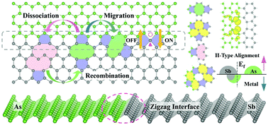
Using detailed first-principles calculations, we investigated the behaviour of interface vacancies in a lateral heterostructure (LHS) constructed by arsenene (As) and antimonene (Sb), which has been demonstrated to have many unique properties but with a large lattice mismatch [Q. Sun, Y. Dai, Y. Ma, N. Yin, W. Wei, L. Yu and B. Huang, 2D Mater., 2016, 3, 035017]. Our calculated results show that the energetics, kinetics and electronic properties of the atomic vacancies are greatly modified at the interface of the As–Sb LHS. Two mechanisms are demonstrated to govern the migration of interfacial DV-585s based on the dissociation/recombination of SVs and the exchange of atoms adjacent to the vacant sites, respectively. DV-5-585 is identified as the lowest-energy atomic vacancy at the interface. The easy formation of DV-5-585 due to the release of the compressed stress in the Sb block suggests that, in LHSs with a large lattice mismatch, much attention should be paid to the potentially large concentration of detrimental interfacial vacancies close to the compressed building blocks, where the proper selection of temperature and careful control of the atomic chemical potential are essential. Meanwhile the unexpected half-metal states induced by DV-3-585-o and DV-4-585-o rooted in the unpaired As atoms driven by the tensile stress reveal that decorating atomic vacancies in the stretched building blocks may provide an effective way to achieve the functionalization of LHSs with a large lattice mismatch. In addition, we reveal a single-atom-triggered transition between the metal and semiconductor in SV-As-1-decorated As–Sb LHS. Thus, by manipulating the Sb atom at the interface, the defect of SV-As-1 may be used as an atomic switch to control the on–off states of a circuit at the nanoscale, making As–Sb LHS a promising candidate for application in nanoelectronic devices. Our theoretical work enriches the fundamental understanding of intrinsic defects at the interface of As–Sb LHSs, and provides significant insight towards defect and interface engineering in LHSs with a large lattice mismatch, which are of great relevance for the manipulation of the LHS properties for the design of novel nanodevices.
 Please wait while we load your content...

