
Morphology of X-ray detector Cs2TeI6 perovskite thick films grown by electrospray method

Abstract
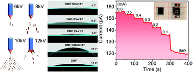
For the purpose of developing Cs2TeI6 based X-ray detectors and imaging devices, Cs2TeI6 thick films were prepared using the electrospray method under ambient conditions. The effects of spraying parameters on the morphology of the films were investigated. During the electrospray process, we observed that Cs2TeI6 microdroplets changed to a steady cone jet and then to an unstable multi-jet model as the electrical bias increased from 6 kV to 12 kV, resulting in variable film morphologies. Five representative solvent systems with different evaporation rates and contact angles on the FTO/double-TiO2 substrates were studied. We find a strong correlation of the contact angle with the speed of primary nucleation, growth mode and subsequent film morphology. Moreover, the crystalline quality has been improved with the rise of substrate temperature. Finally, a dense and uniform Cs2TeI6 film was obtained with an electrical bias of 10 kV using dimethyl formamide (DMF) as the solvent at a substrate temperature of 160 °C. The resulting Cs2TeI6 films have resistivity on the order of 1010 Ω cm, which indicates potential applications in X-ray detection and imaging. The films show a strong photoresponse to visible light based on the Cs2TeI6 thick film devices, and an on–off ratio of 22 under 425 nm light (∼65 mW cm−2). The sensitivity of the assembled Cs2TeI6 perovskite-based detectors can be 2.4 nC R−1 cm−2 under illumination of 60 kVp X-rays.
 Please wait while we load your content...

