
Chemical durability engineering of solution-processed oxide thin films and its application in chemically-robust patterned oxide thin-film transistors†
Abstract
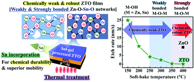
For the fabrication of solution-processed oxide thin-film transistors (TFTs), most studies have focused on the sol–gel coating of oxide films with high mobility, but the inevitable wet-based channel or metal patterning processes to integrate the circuits (individual TFTs + metal-lines) on large-area TFT back-planes have been excluded due to unintentional electrical degradation of conventional In and Zn based oxide channels and additional post-processes (etch-stopper and recovery process). The incorporation of Sn–O bonds in oxide films can enhance their electrical performance and chemical durability and minimize electrical degradation during wet-based metal patterning, but conversely, it makes wet-based channel patterning difficult. Using Sn–O incorporation and temperature-controlled thermal annealing, based on the chemical reaction route, we were able to engineer the chemical durability of sol–gel coated Sn-incorporated ZnO (ZTO) films into inferior (with weak M–O bonds) and robust states (with strong M–O bonds). Well-patterned solution-processed ZTO channels were formed in a chemically weak state and reinforced into a chemically robust state for metal patterning via the combination (soft-bake → pattern → hard bake) of chemical durability engineering and a wet-etching process, which induced uniformly patterned, highly electrical, chemically robust ZTO channels with a low leakage current (∼1011 A), superior electrical performance (2.0 ≤ μFE ≤ 3.2 cm2 V−1 s−1), and chemical robustness against metal wet etchants. All wet-based approaches are designed to integrate the circuits (individual TFTs + metal-lines) on large-area solution-processed oxide TFT back-planes: (i) sol–gel channel coating, (ii) channel wet patterning, and (iii) electrode wet patterning in solution systems.
 Please wait while we load your content...

