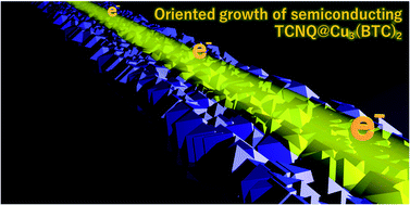
Oriented growth of semiconducting TCNQ@Cu3(BTC)2 MOF on Cu(OH)2: crystallographic orientation and pattern formation toward semiconducting thin-film devices†

Abstract
The host–guest system TCNQ@Cu3(BTC)2 (TCNQ = 7,7,8,8-tetracyanoquinodimethane, BTC = 1,3,5-benzenetricarboxylate) exhibits semiconducting properties with potential applications in thin-film devices, such as field-effect transistors and thermoelectric films. Although controlling its crystallographic orientation is important for the efficient use of its electrical properties in advanced semiconductors, the fabrication of Cu3(BTC)2 thin films with both in-plane and out-of-plane orientations (three-dimensionally oriented thin films) remains a challenge. Here, we report on the fabrication of three-dimensionally oriented Cu3(BTC)2 thin films via heteroepitaxial growth on Cu(OH)2. The epitaxial growth direction of Cu3(BTC)2 is determined by lattice matching at the Cu3(BTC)2/Cu(OH)2 interface and interface bonding (local chemical connection matching; spatial matching of Cu atoms across the interface). The epitaxial growth approach enables the fabrication of oriented TCNQ@Cu3(BTC)2 thin films, where the {111} lattice plane, which can be a conducting path, is oriented both parallel and perpendicular to the substrate. Owing to the in-plane orientation of the {111} lattice plane in the oriented TCNQ@Cu3(BTC)2 film, we have, for the first time, achieved MOF thin films with anisotropic electrical properties in the in-plane direction. Moreover, we show that it is possible to fabricate oriented MOF patterns by integration with UV lithography technology. The oriented MOF patterns with anisotropic conduction will pave the way for next-generation smart electronic devices.
- This article is part of the themed collections: Journal of Materials Chemistry A Lunar New Year collection 2022, Journal of Materials Chemistry A HOT Papers and Journal of Materials Chemistry A Emerging Investigators
 Please wait while we load your content...

